
A Multichannel, High-Bandwidth Wirelane Receiver for D2D Interconnects


Abstract
:1. Introduction
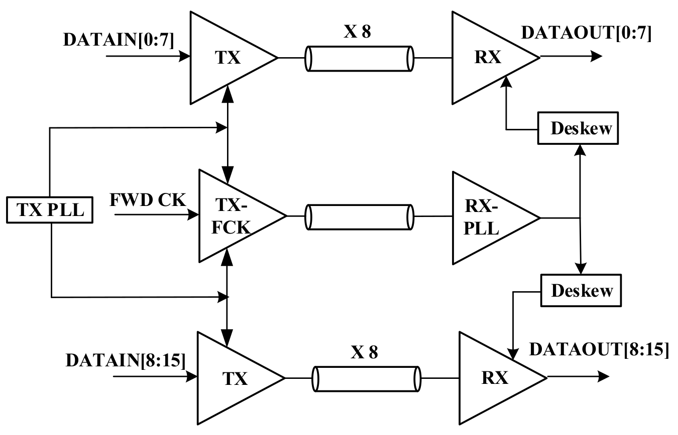
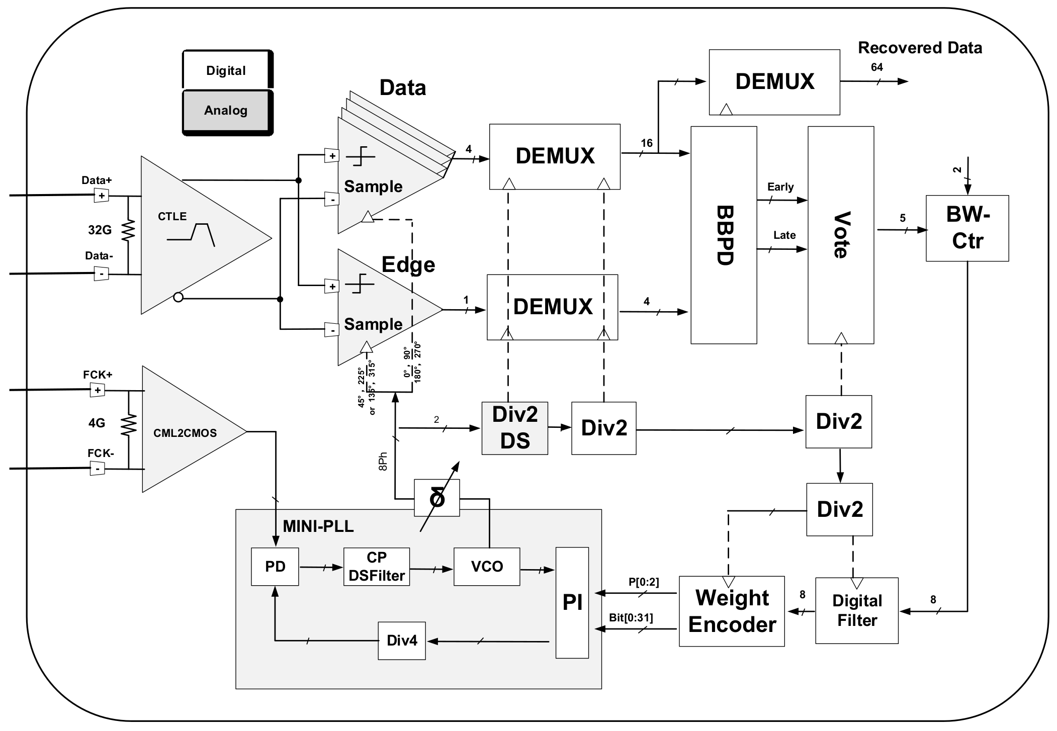
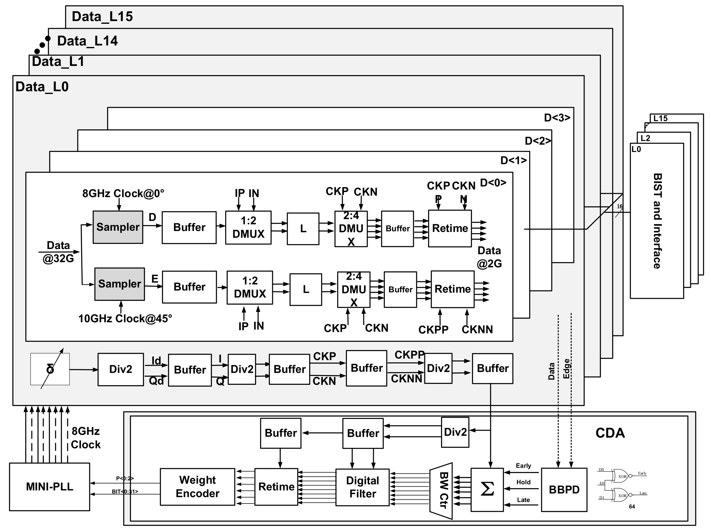
2. Receiver Design
2.1. CDA
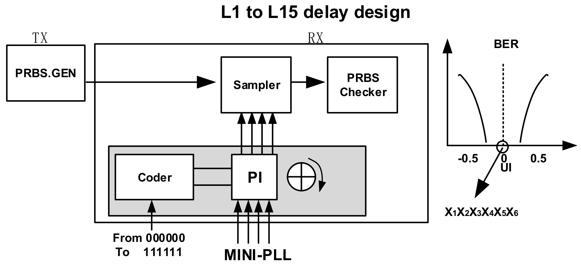
2.2. Delay Matching
3. Receiver Circuits
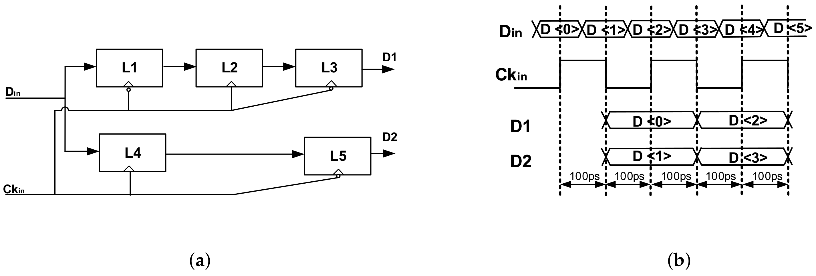
3.1. DMUX1:2
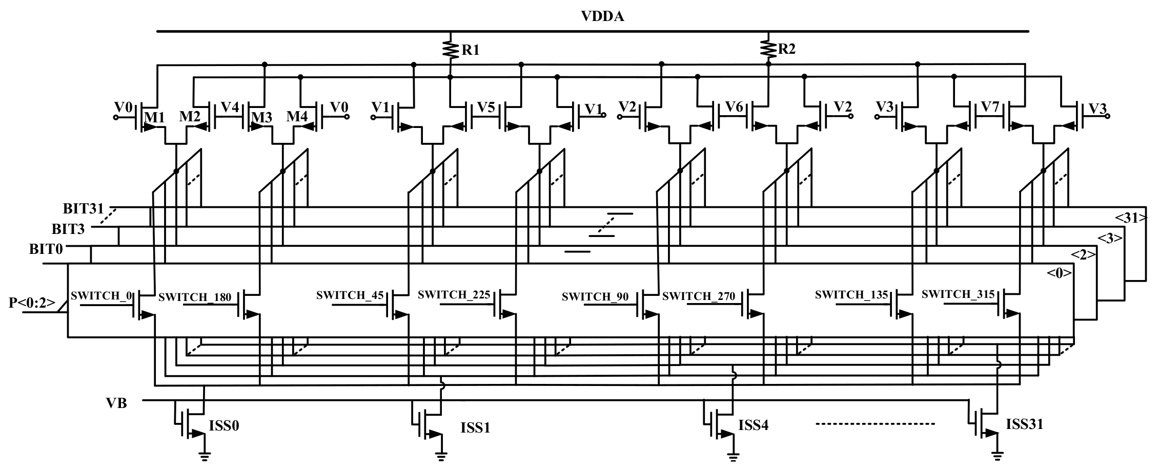
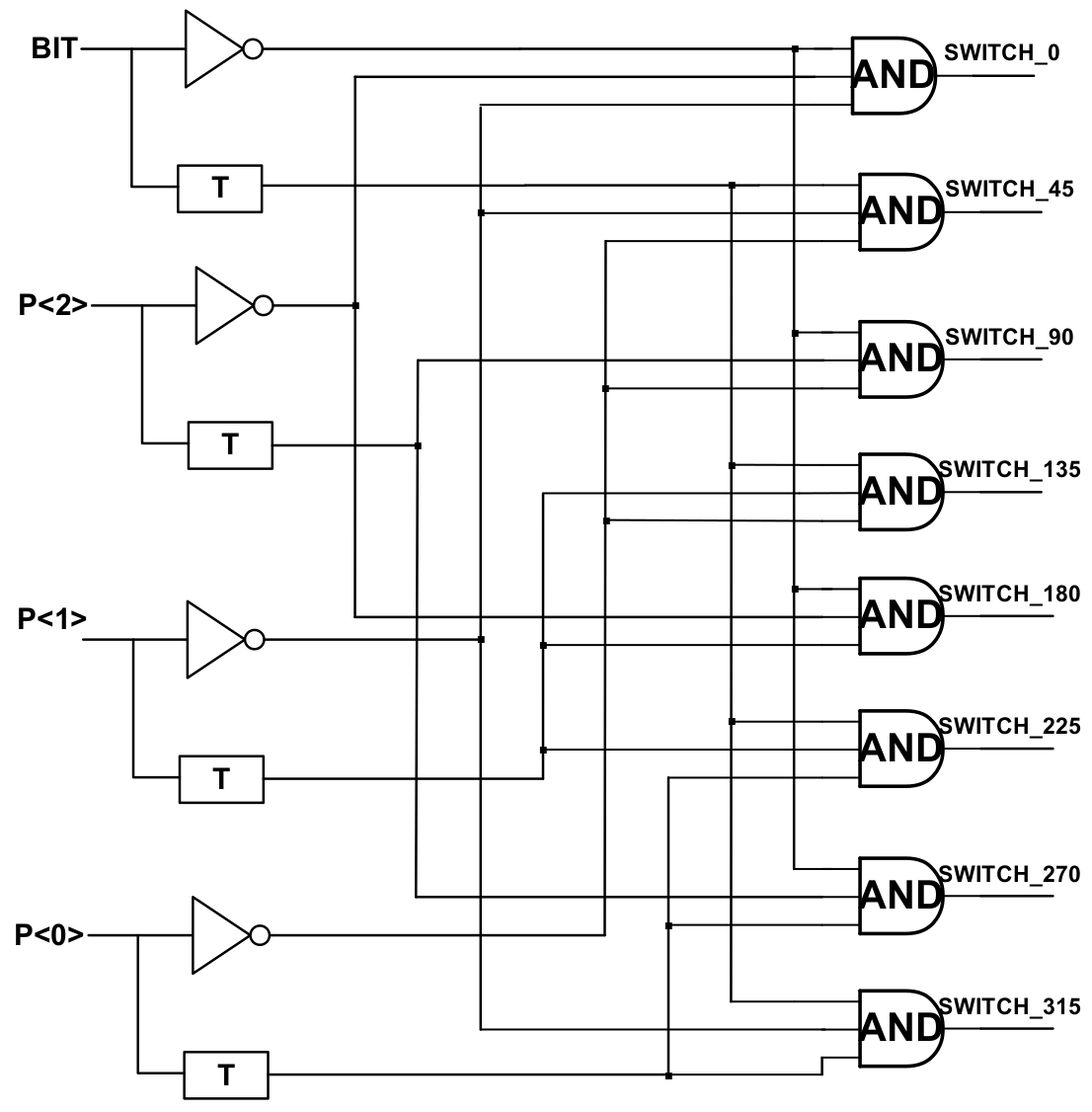
3.2. CDA Design
3.2.1. Digital Model
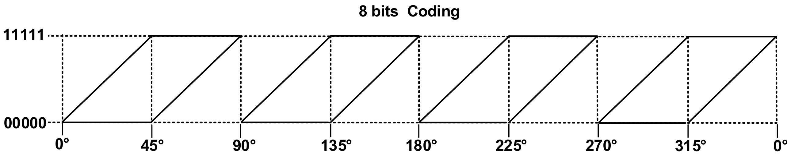
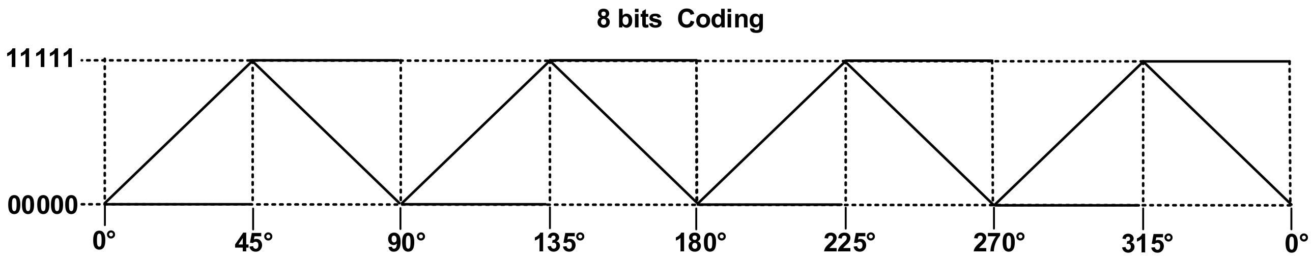
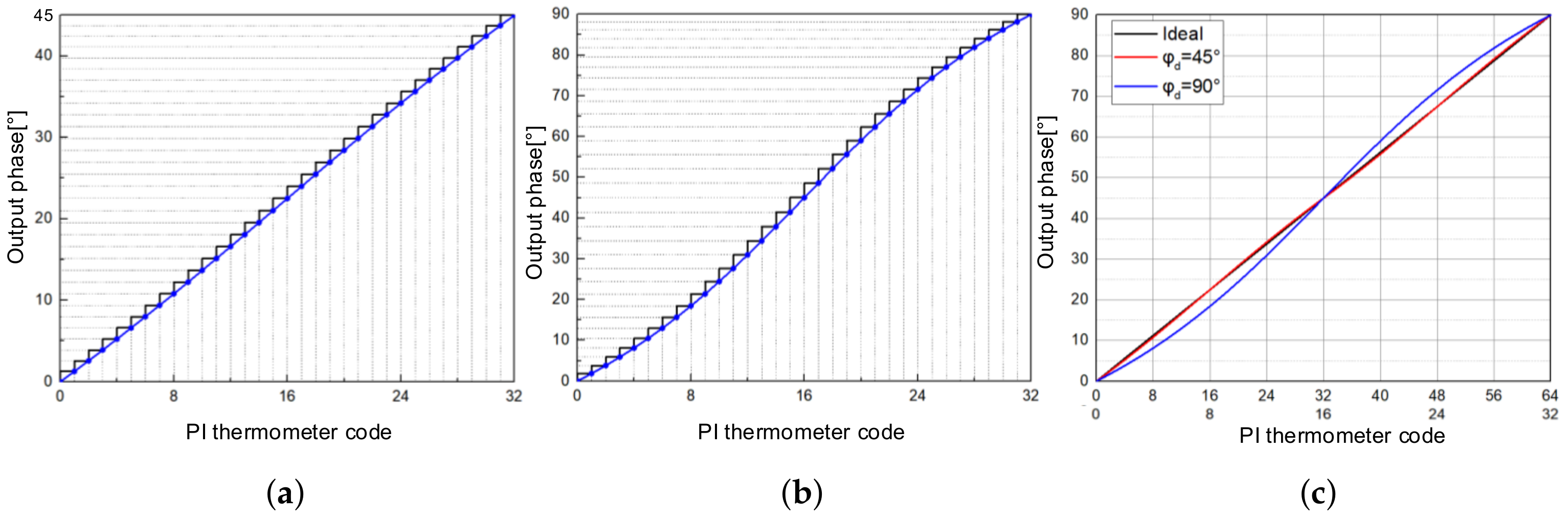
3.2.2. Weight Coding
3.3. MINI-PLL
3.3.1. Design
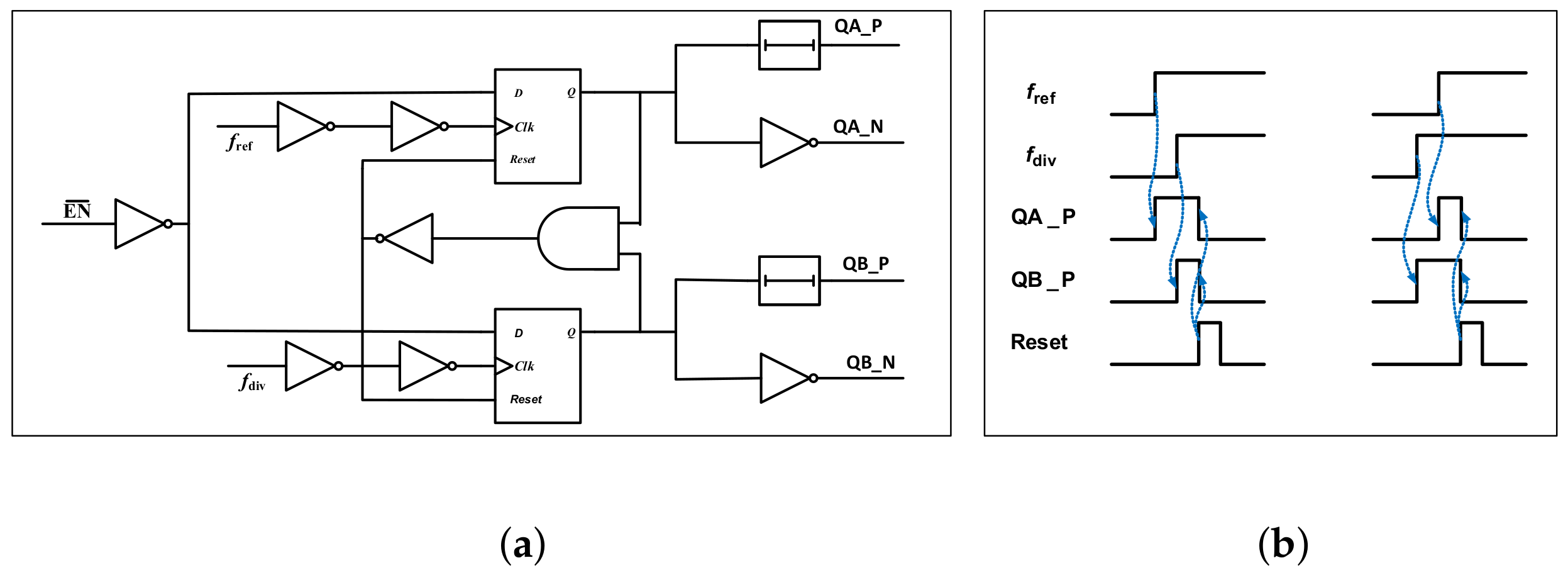
3.3.2. PFD
3.3.3. Charge Pump
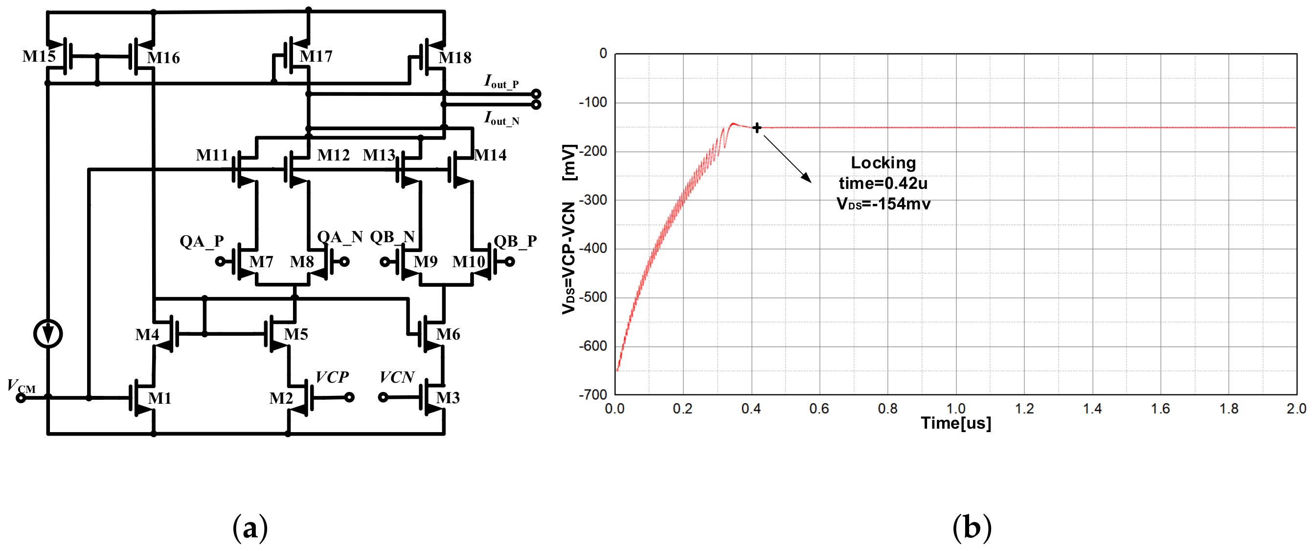
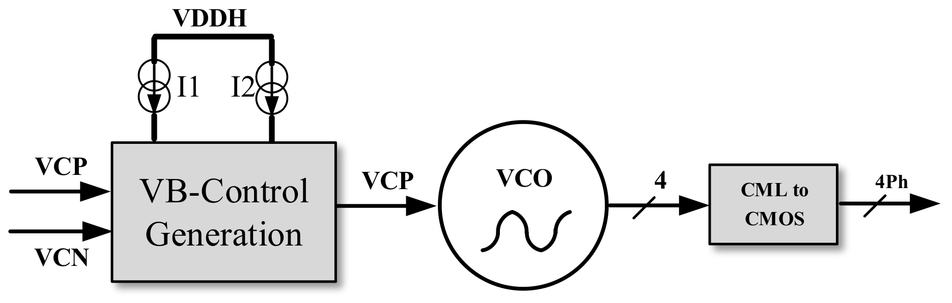
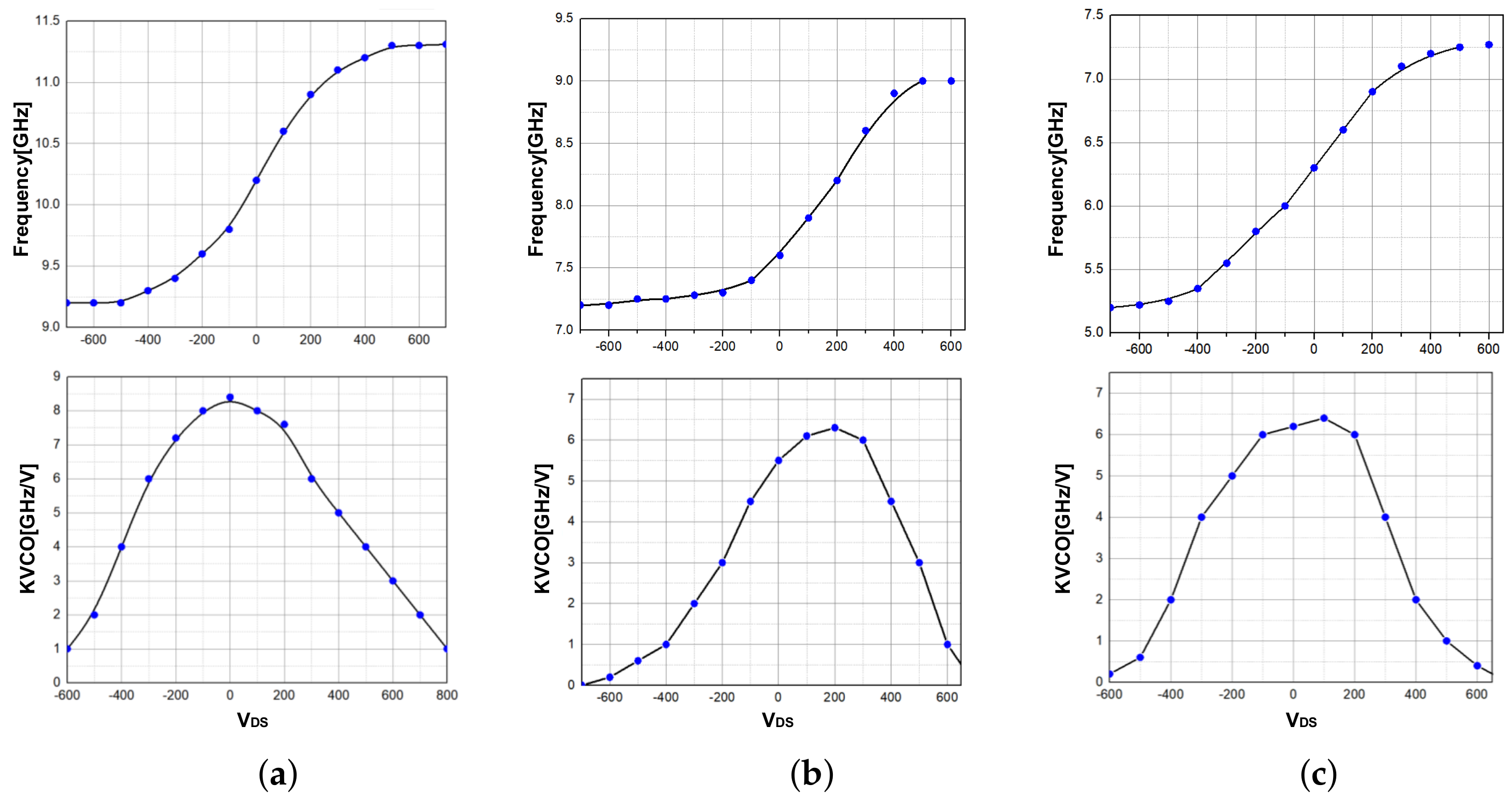
3.3.4. VCO
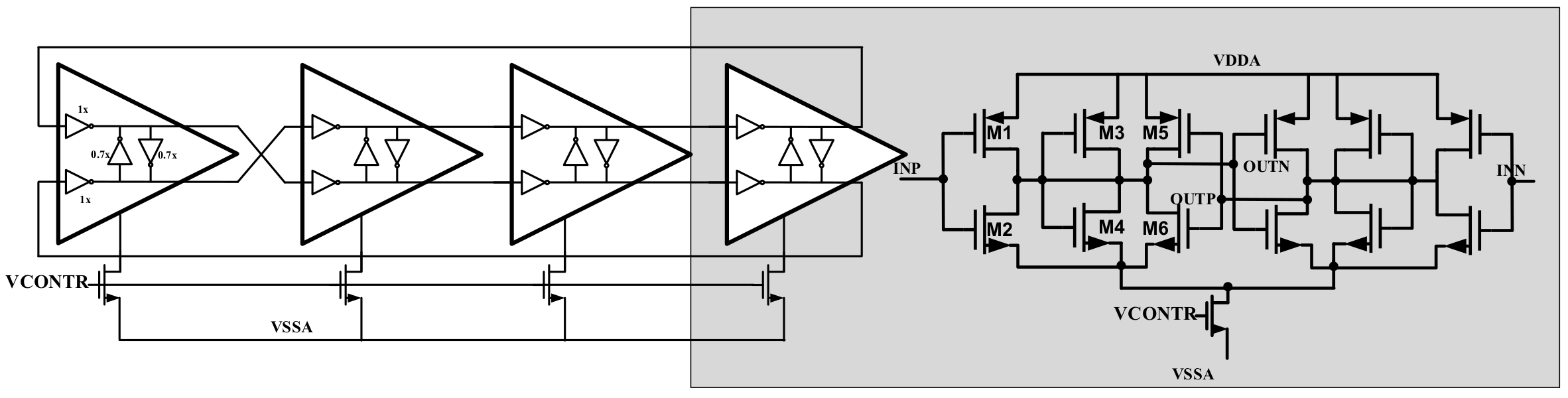
3.3.5. PI
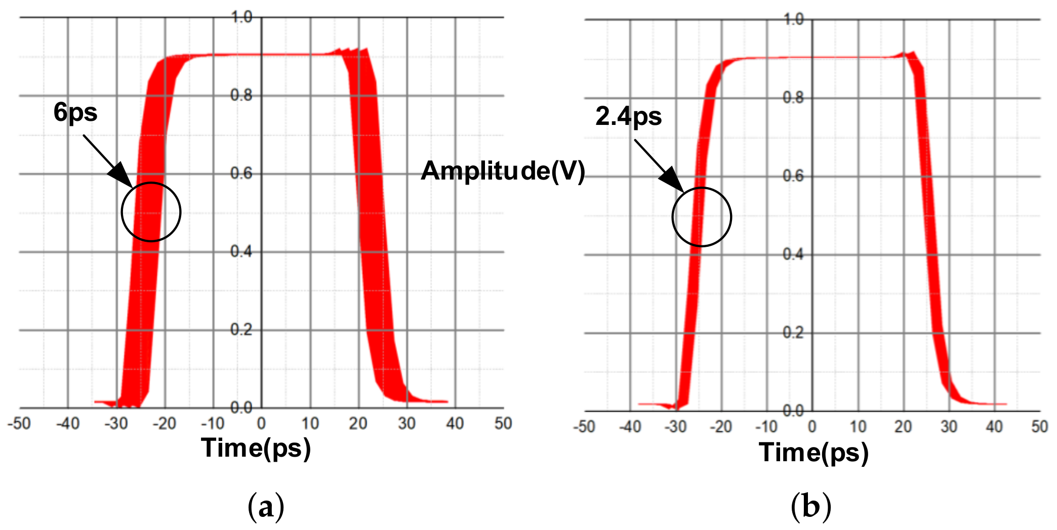
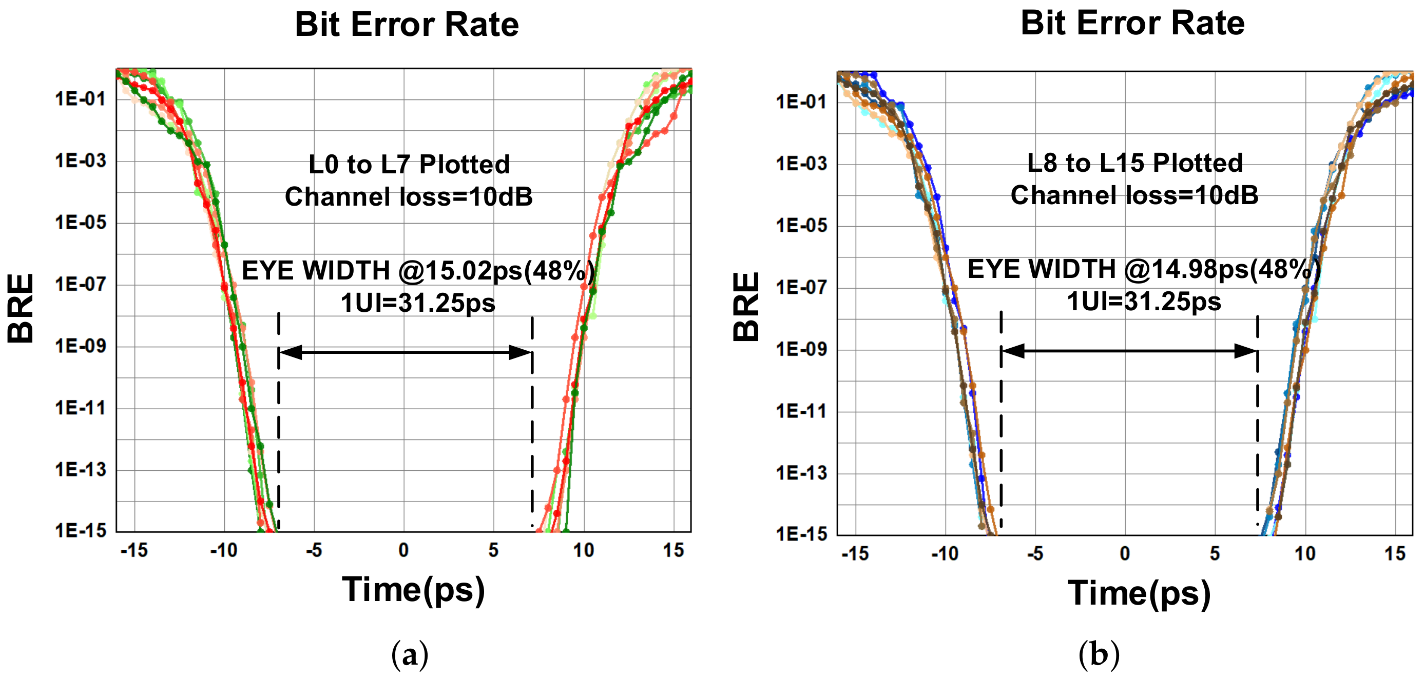
4. Results
5. Conclusions
Author Contributions
Funding
Conflicts of Interest
References
- Hutner, M.; Sethuram, R.; Vinnakota, B.; Armstrong, D.; Copperhall, A. Special Session: Test Challenges in a Chiplet Marketplace. In Proceedings of the 2020 IEEE 38th VLSI Test Symposium (VTS), San Diego, CA, USA, 5–8 April 2020; pp. 1–12. [Google Scholar] [CrossRef]
- Farjadrad, R.; Vinnakota, B. A Bunch of Wires (BoW) Interface for Inter-Chiplet Communication. In Proceedings of the 2019 IEEE Symposium on High-Performance Interconnects (HOTI), Santa Clara, CA, USA, 14–16 August 2019; pp. 27–273. [Google Scholar] [CrossRef]
- Shivnaraine, R.; van Ierssel, M.; Farzan, K.; Diclemente, D.; Ng, G.; Wang, N.; Musayev, J.; Dutta, G.; Shibata, M.; Moradi, A.; et al. 11.2 A 26.5625-to-106.25Gb/s XSR SerDes with 1.55pJ/b Efficiency in 7nm CMOS. In Proceedings of the 2021 IEEE International Solid- State Circuits Conference (ISSCC), San Francisco, CA, USA, 13–22 February 2021; pp. 181–183. [Google Scholar] [CrossRef]
- Loh, M.; Emami-Neyestanak, A. A 3x9 Gb/s Shared, All-Digital CDR for High-Speed, High-Density I/O. IEEE J. Solid-State Circuits 2012, 47, 641–651. [Google Scholar] [CrossRef]
- Liu, C.; Botimer, J.; Zhang, Z. A 256Gb/s/mm-shoreline AIB-Compatible 16nm FinFET CMOS Chiplet for 2.5D Integration with Stratix 10 FPGA on EMIB and Tiling on Silicon Interposer. In Proceedings of the CICC, Austin, TX, USA, 25–30 April 2021; pp. 1–2. [Google Scholar]
- Lin, M.S.; Huang, T.C.; Tsai, C.C.; Tam, K.H.; Hsieh, K.C.; Chen, C.F.; Huang, W.H.; Hu, C.W.; Chen, Y.C.; Goel, S.K.; et al. A 7-nm 4-GHz Arm-Core-Based CoWoS Chiplet Design for High-Performance Computing. IEEE J. Solid-State Circuits 2020, 55, 956–966. [Google Scholar] [CrossRef]
- Zhou, G.; Zhou, L.; Guo, Y.; Chen, S.; Lu, L.; Liu, L.; Chen, J. 32-Gb/s OOK and 64-Gb/s PAM-4 Modulation Using a Single-Drive Silicon Mach–Zehnder Modulator with 2 V Drive Voltage. IEEE Photonics J. 2019, 11, 6603610. [Google Scholar] [CrossRef]
- Poulton, J.W.; Dally, W.J.; Chen, X.; Eyles, J.G.; Greer, T.H.; Tell, S.G.; Wilson, J.M.; Gray, C.T. A 0.54 pJ/b 20 Gb/s Ground-Referenced Single-Ended Short-Reach Serial Link in 28 nm CMOS for Advanced Packaging Applications. IEEE J. Solid-State Circuits 2013, 48, 3206–3218. [Google Scholar] [CrossRef]
- Chung, S.; Kim, L. 1.22mW/Gb/s 9.6Gb/s data jitter mixing forwarded-clock receiver robust against power noise with 1.92ns latency mismatch between data and clock in 65nm CMOS. In Proceedings of the 2012 Symposium on VLSI Circuits (VLSIC), Honolulu, HI, USA, 13–15 June 2012; pp. 144–145. [Google Scholar] [CrossRef]
- Chen, S.; Li, H.; Chiang, P.Y. A Robust Energy/Area-Efficient Forwarded-Clock Receiver With All-Digital Clock and Data Recovery in 28-nm CMOS for High-Density Interconnects. IEEE Trans. Very Large Scale Integr. (Vlsi) Syst. 2016, 24, 578–586. [Google Scholar] [CrossRef]
- Universal Chiplet Interconnect Express (UCIe) Specification Revision 1.0. 2022. Available online: https://www.uciexpress.org/specification (accessed on 30 February 2022).
- Chung, C.-C.; Lee, C.-Y. A new DLL-based approach for all-digital multiphase clock generation. IEEE J. Solid-State Circuits 2004, 39, 469–475. [Google Scholar] [CrossRef]
- Tajalli, A.; Bastani, M.; Carnelli, D.; Cao, C.; Fox, J.; Gharibdoust, K.; Gorret, D.; Gupta, A.; Hall, C.; Hassanin, A.; et al. A 1.02pJ/b 417Gb/s/mm USR Link in 16nm FinFET. In Proceedings of the 2019 Symposium on VLSI Circuits, Kyoto, Japan, 9–14 June 2019; pp. C92–C93. [Google Scholar] [CrossRef]
- Kanda, K. 40Gb/s 4:1 MUX/1:4 DEMUX in 90nm standard CMOS. In Proceedings of the ISSCC 2005 IEEE International Digest of Technical Papers. Solid-State Circuits Conference, San Francisco, CA, USA, 10 February 2005; Volume 1, pp. 152–590. [Google Scholar] [CrossRef]
- Bae, W.; Ju, H.; Park, K.; Cho, S.; Jeong, D. A 7.6 mW, 214-fs RMS jitter 10-GHz phase-locked loop for 40-Gb/s serial link transmitter based on two-stage ring oscillator in 65-nm CMOS. In Proceedings of the 2015 IEEE Asian Solid-State Circuits Conference (A-SSCC), Xia’men, China, 9–11 November 2015; pp. 1–4. [Google Scholar] [CrossRef]
- IEEE Std 1241-2000; IEEE Standard for Terminology and Test Methods for Analog-to-Digital Converters. IEEE: Piscataway, NJ, USA, 2001; pp. 1–98. [CrossRef]
- Chen, M.-S.; Hafez, A.A.; Yang, C.-K.K. A 0.1–1.5 GHz 8-bit inverter-based digital-to-phase converter using harmonic rejection. In Proceedings of the 2012 IEEE Asian Solid State Circuits Conference (A-SSCC), Kobe, Japan, 12–14 November 2012; pp. 145–148. [Google Scholar] [CrossRef]
- Ravi, A.; Madoglio, P.; Xu, H.; Chandrashekar, K.; Verhelst, M.; Pellerano, S.; Cuellar, L.; Aguirre-Hernandez, M.; Sajadieh, M.; Zarate-Roldan, J.E.; et al. A 2.4-GHz 20–40-MHz Channel WLAN Digital Outphasing Transmitter Utilizing a Delay-Based Wideband Phase Modulator in 32-nm CMOS. IEEE J. Solid-State Circuits 2012, 47, 3184–3196. [Google Scholar] [CrossRef]
- Erett, M.; Carey, D.; Hudner, J.; Casey, R.; Geary, K.; Neto, P.; Raj, M.; McLeod, S.; Zhang, H.; Roldan, A.; et al. A 126mW 56Gb/s NRZ wireline transceiver for synchronous short-reach applications in 16nm FinFET. In Proceedings of the 2018 IEEE International Solid-State Circuits Conference—(ISSCC), San Francisco, CA, USA, 11–15 February 2018; pp. 274–276. [Google Scholar] [CrossRef]
- Shibasaki, T.; Danjo, T.; Ogata, Y.; Sakai, Y.; Miyaoka, H.; Terasawa, F.; Kudo, M.; Kano, H.; Matsuda, A.; Kawai, S.; et al. 3.5 A 56Gb/s NRZ-electrical 247mW/lane serial-link transceiver in 28nm CMOS. In Proceedings of the 2016 IEEE International Solid-State Circuits Conference (ISSCC), San Francisco, CA, USA, 31 January–4 February 2016; pp. 64–65. [Google Scholar] [CrossRef]
- Wilson, J.M.; Turner, W.J.; Poulton, J.W.; Zimmer, B.; Chen, X.; Kudva, S.S.; Song, S.; Tell, S.G.; Nedovic, N.; Zhao, W.; et al. A 1.17pJ/b 25Gb/s/pin ground-referenced singleended serial link for off- and on-package communication in 16nm CMOS using a process-and temperature-adaptive voltage regulator. In Proceedings of the 2018 IEEE International Solid-State Circuits Conference—(ISSCC), San Francisco, CA, USA, 11–15 February 2018; pp. 276–278. [Google Scholar]


| P<2:0> | 000 | 001 | 011 | 010 | 110 | 111 | 101 | 100 |
| Ph[] | 0–45 | 45–90 | 90–135 | 135–180 | 180–225 | 225–270 | 270–315 | 315–360(0) |
| BIT | 5-bit | BIT | 5-bit | BIT | |
|---|---|---|---|---|---|
| 31 | A | 20 | (+) | 9 | +(++) |
| 30 | 19 | (++) | 8 | + | |
| 29 | (+) | 18 | (++) | 7 | ++ |
| 28 | 17 | (+++) | 6 | ++ | |
| 27 | (+) | 16 | 5 | ++(+) | |
| 26 | (+) | 15 | + | 4 | ++ |
| 25 | (++) | 14 | + | 3 | +++ |
| 24 | 13 | +(+) | 2 | +++ | |
| 23 | (+) | 12 | + | 1 | ++++ |
| 22 | (+) | 11 | +(+) | 0 | |
| 21 | (+(+)) | 10 | +(+) |
| Type | DNL | INL | Power Consumtion | Precision | Technology |
|---|---|---|---|---|---|
| [17] | 0.89 LSB | 2.18 LSB | 3.4 mW | 8 bit | 65 nm |
| [18] | — | 1.64 LSB | — | 8 bit | 32 nm |
| This work | 0.54 LSB | 0.68 LSB | 10 mW | 8 bit | 28 nm |
| Reference | [19] | [20] | [21] | [8] | This work |
|---|---|---|---|---|---|
| Signaling | DS | DS | SES | SES | DS |
| Date Rate (Gb/s) | 56 | 56.2 | 25 | 20 | 32 |
| Insertion loss (dB) | 11 | 18.4 | 8.5 | 1 | 10 |
| Technology (nm) | 16 | 28 | 16 | 28 | 28 |
| Energy Efficiency (pJ/b) | 2.25 | 4.4 | 1.17 | 0.54 | 1.56 |
| BRE | 10−15 | 10−15 | 10−15 | 10−12 | 10−12 |
| Core area (RX+TX) [mm2] | 2.64 | 1.4 | 0.75 | 1.2 | 1.8 |
| Throughput (RX+TX) Gb/s | 448 | 112.4 | 200 | 320 | 512 |
| Density of BW Gb/s/mm | 169 | 80.2 | 266.7 | 266.7 | 284 |
Publisher’s Note: MDPI stays neutral with regard to jurisdictional claims in published maps and institutional affiliations. |
© 2022 by the authors. Licensee MDPI, Basel, Switzerland. This article is an open access article distributed under the terms and conditions of the Creative Commons Attribution (CC BY) license (https://creativecommons.org/licenses/by/4.0/).
Share and Cite
Zhang, G.; Lai, M.; Lyu, F. A Multichannel, High-Bandwidth Wirelane Receiver for D2D Interconnects. Electronics 2022, 11, 2864. https://doi.org/10.3390/electronics11182864
Zhang G, Lai M, Lyu F. A Multichannel, High-Bandwidth Wirelane Receiver for D2D Interconnects. Electronics. 2022; 11(18):2864. https://doi.org/10.3390/electronics11182864
Chicago/Turabian StyleZhang, Geng, Mingche Lai, and Fangxu Lyu. 2022. "A Multichannel, High-Bandwidth Wirelane Receiver for D2D Interconnects" Electronics 11, no. 18: 2864. https://doi.org/10.3390/electronics11182864