
Research on Automotive Bidirectional CLLC Resonant Converters Based on High-Order Sliding Mode Control

Abstract
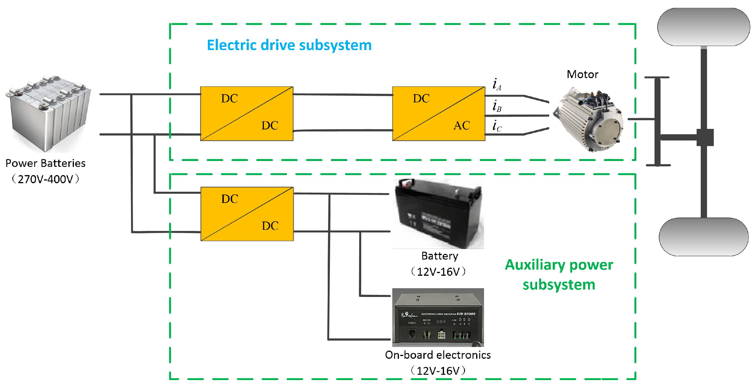
:1. Introduction
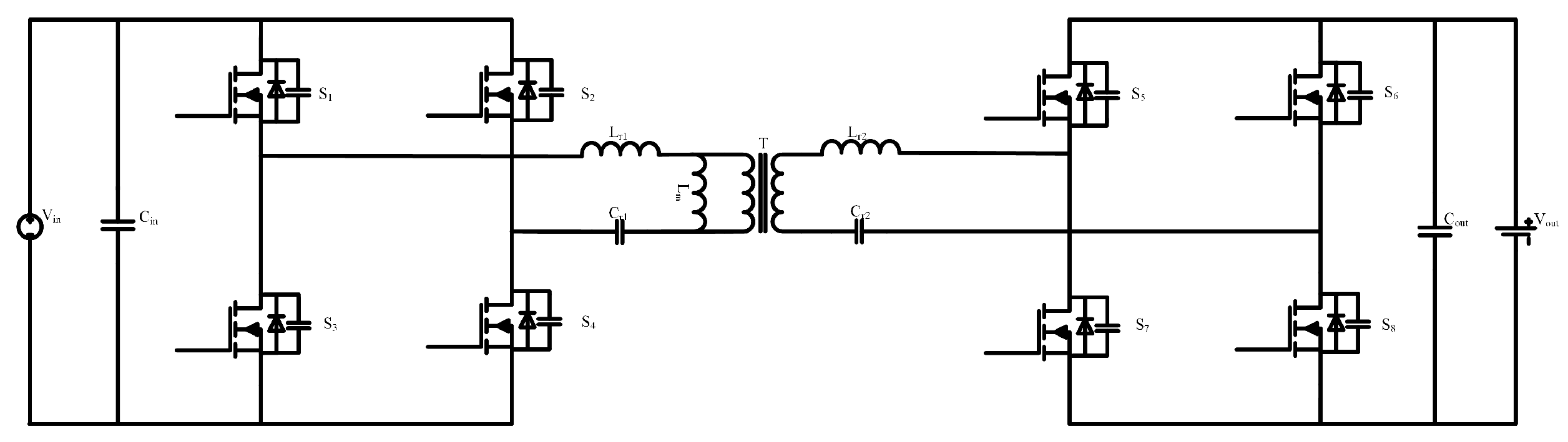
2. Analysis of Automotive Bidirectional Full-Bridge CLLC Resonant Converters
2.1. Analysis of the Topology of Power Main Circuits
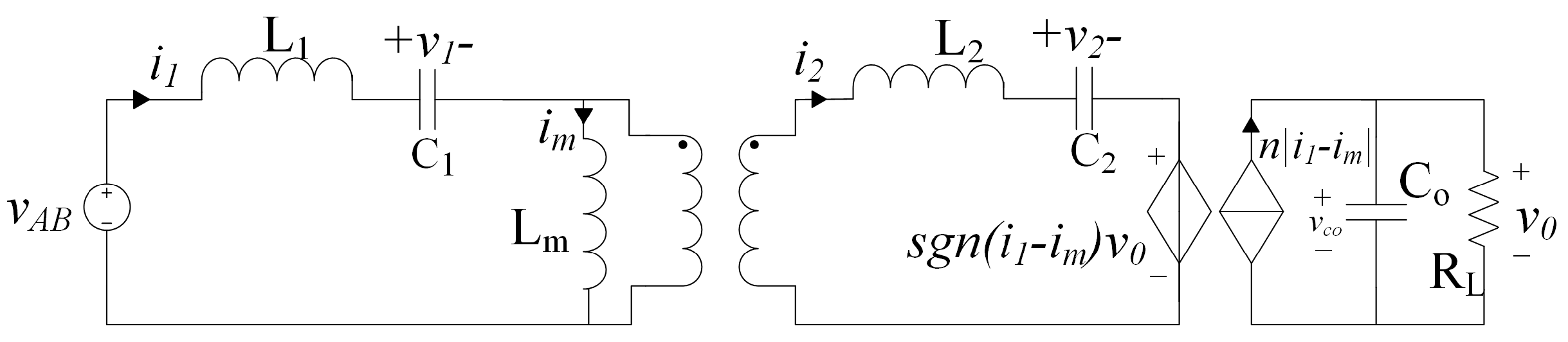
2.2. Modeling Analysis Based on the EDF Method
2.2.1. Nonlinear Equation of State for CLLC Resonant Converters
2.2.2. Harmonic Approximation
2.2.3. Edf Equations
2.2.4. Large-Signal Model for CLLC Resonant Converters
3. SMC of CLLC Resonant Converters
3.1. Basic Principles of Sliding Mode Control
- Conditions of arrival: regardless of where the trajectory starts, the arrival condition directs the state trajectory to the sliding surface, as shown in stages A–B in Figure 4. Depending on the conditions of the termination point, it follows that:
- Conditions of existence: This condition ensures that once the system trajectory has reached the sliding surface, the trajectory can continue to start the sliding motion on the sliding surface, as shown in stages B–C in Figure 4. The existence condition can be determined simply by testing the conditions of arrival, i.e., by satisfying Equation (9).
- Conditions of stability: The conditions of stability ensure that the sliding surface is always able to drive the trajectory towards a stable equilibrium point. If the stability conditions are not met, this will result in an unstable sliding system. At this point, the system is satisfying the following mathematical model:
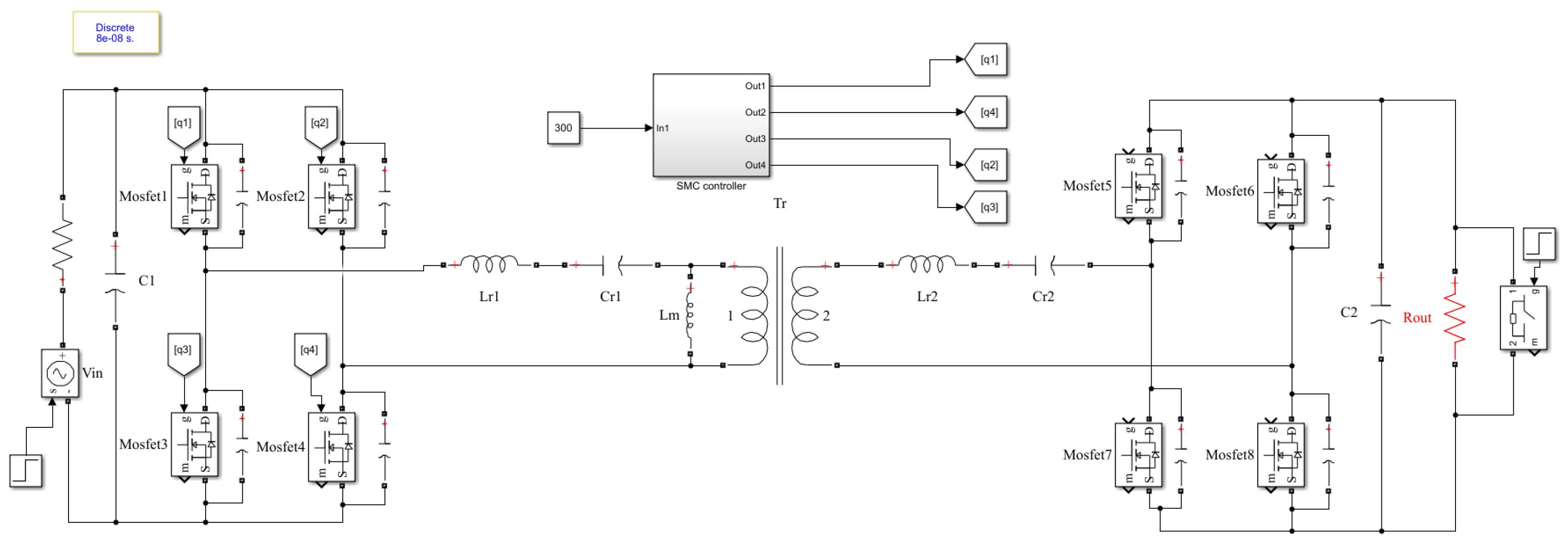
3.2. Sliding Mode Controller for CLLC Resonant Converters
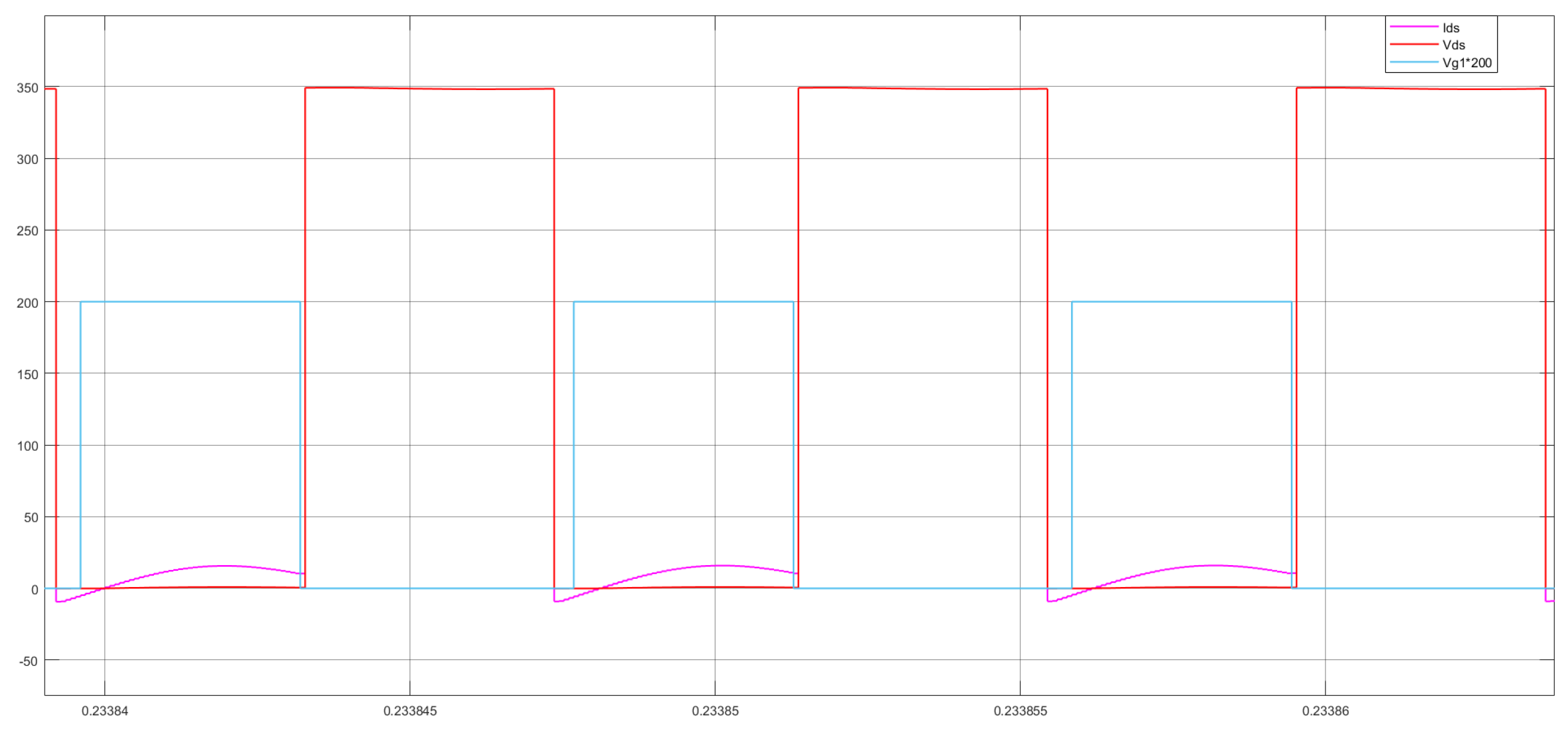
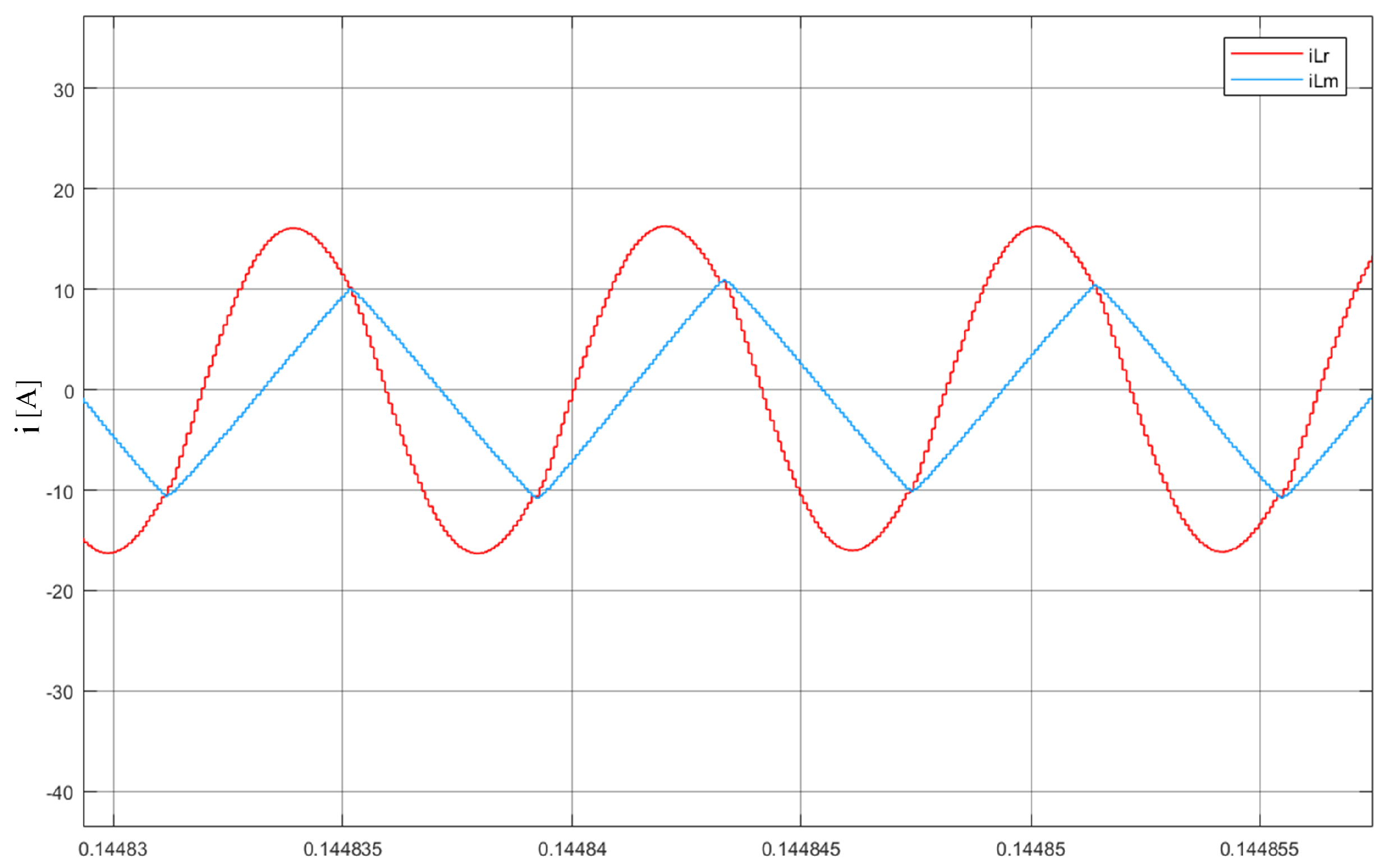
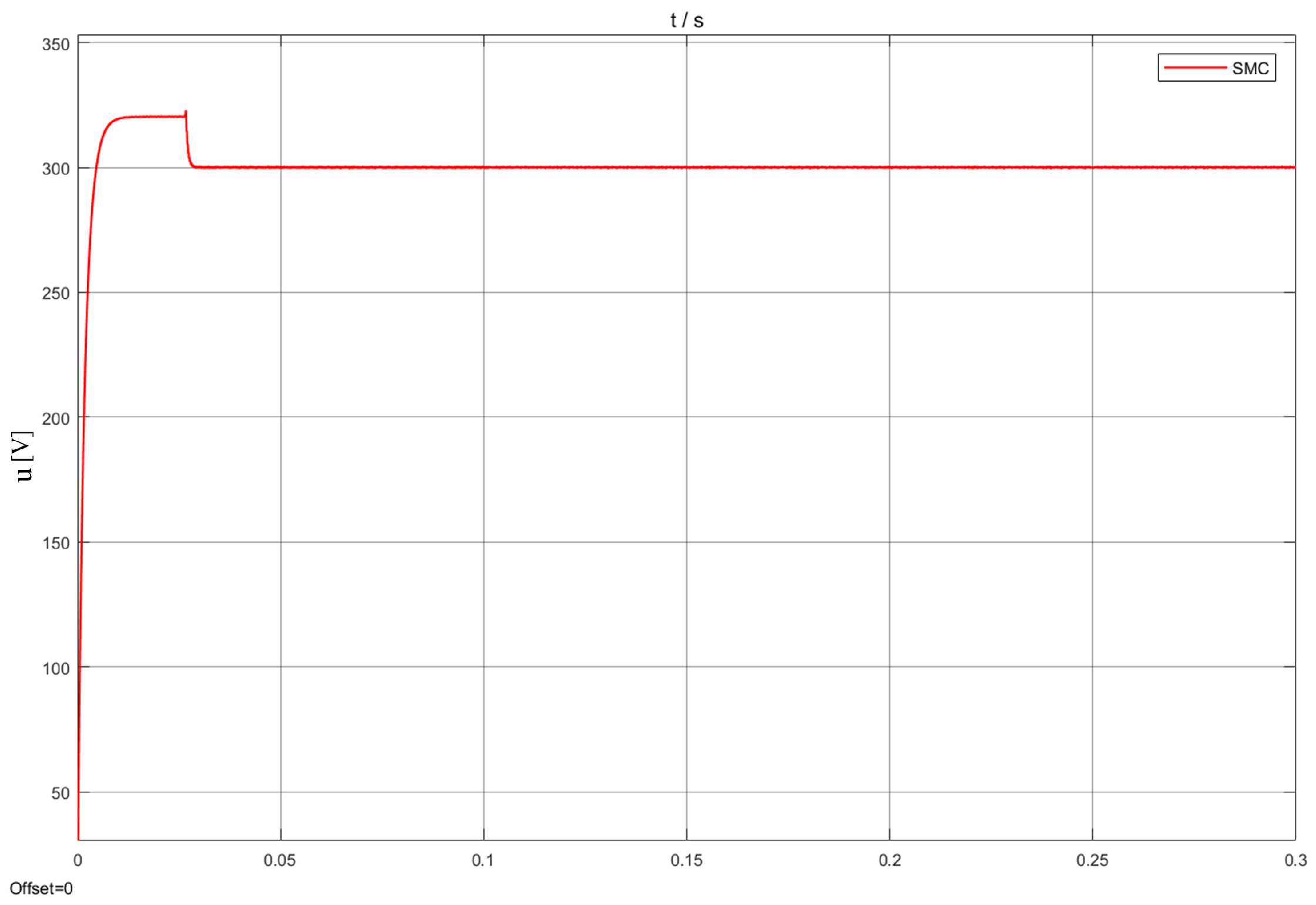
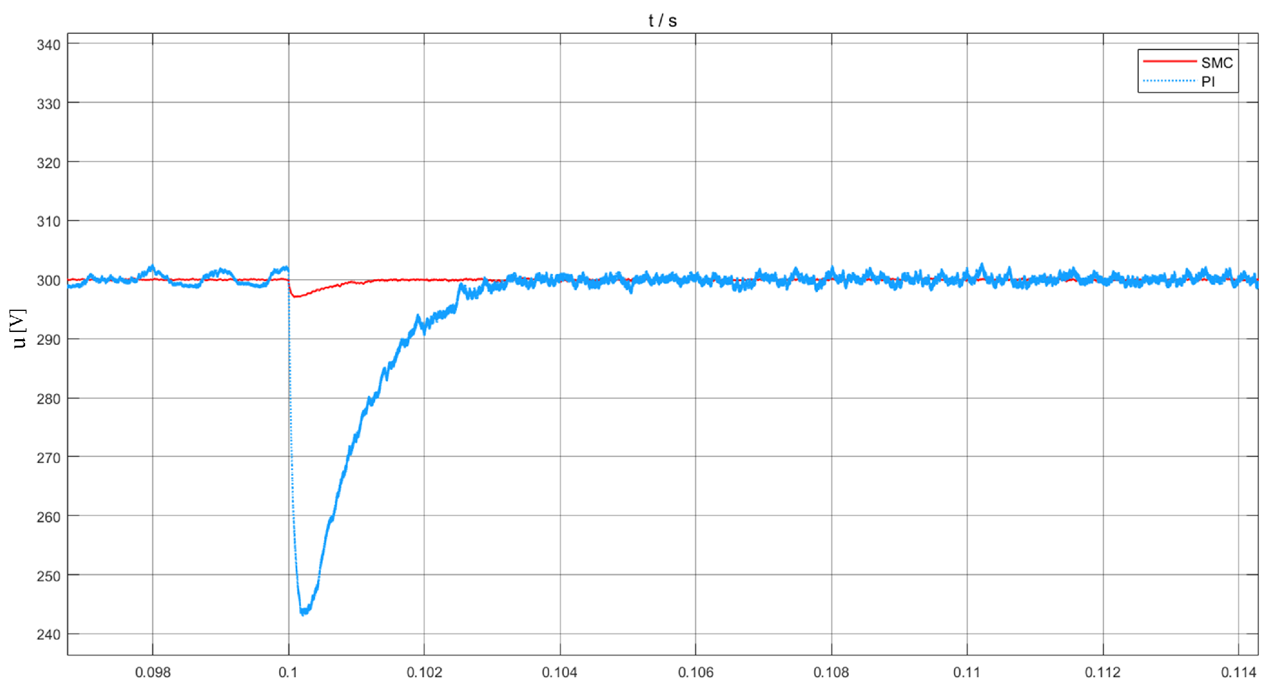
4. Analysis of Simulation and Experimental Results
5. Conclusions
Author Contributions
Funding
Acknowledgments
Conflicts of Interest
References
- Park, K.; Lee, K.-B. A Bidirectional Double Uneven Power Converter Based DC–DC Converter for Solid-State Transformers. Electronics 2018, 7, 334. [Google Scholar] [CrossRef]
- Lin, B.-R.; Lin, G.-H.; Jian, A. Resonant Converter with Voltage-Doubler Rectifier or Full-Bridge Rectifier for Wide-Output Voltage and High-Power Applications. Electronics 2019, 8, 3. [Google Scholar] [CrossRef]
- Li, X.; Huang, J.; Ma, Y.; Wang, X.; Yang, J.; Wu, X. Unified Modeling, Analysis, and Design of Isolated Bidirectional CLLC Resonant DC–DC Converters. IEEE J. Emerg. Sel. Top. Power Electron. 2022, 10, 2305–2318. [Google Scholar] [CrossRef]
- Min, J.; Ordonez, M. Bidirectional Resonant CLLC Charger for Wide Battery Voltage Range: Asymmetric Parameters Methodology. IEEE Trans. Power Electron. 2021, 36, 6662–6673. [Google Scholar] [CrossRef]
- Sun, J.; Yuan, L.; Gu, Q.; Duan, R.; Lu, Z.; Zhao, Z. Design-Oriented Comprehensive Time-Domain Model for CLLC Class Isolated Bidirectional DC-DC Converter for Various Operation Modes. IEEE Trans. Power Electron. 2020, 35, 3491–3505. [Google Scholar] [CrossRef]
- Zhao, L.; Pei, Y.; Wang, L.; Pei, L.; Cao, W.; Gan, Y. Design Methodology of Bidirectional Resonant CLLC Charger for Wide Voltage Range Based on Parameter Equivalent and Time Domain Model. IEEE Trans. Power Electron. 2022, 37, 12041–12064. [Google Scholar] [CrossRef]
- He, P.; Mallik, A.; Sankar, A.; Khaligh, A. Design of a 1-MHz High-Efficiency High-Power-Density Bidirectional GaN-Based CLLC Converter for Electric Vehicles. IEEE Trans. Veh. Technol. 2019, 68, 213–223. [Google Scholar] [CrossRef]
- Yu, K.; Zhuo, F.; Wang, F.; Jiang, X. Deep-Learning-Based Steady-State Modeling and Model Predictive Control for CLLC DC-DC Resonant Converter in DC Distribution System. In Proceedings of the 2022 IEEE Applied Power Electronics Conference and Exposition (APEC), Orlando, FL, USA, 19–23 March 2022; pp. 1–5. [Google Scholar]
- Zhu, Q. Design of Converter for Wide Range Battery Charging and Discharging System. Master’s Thesis, Harbin Institute of Technology, Harbin, China, 2020. Available online: https://kns.cnki.net/KCMS/detail/detail.aspx?dbname=CMFD202101&filename=1020396108.nh (accessed on 8 August 2022).
- Li, K. Study on Topology and Control of Wide Gain High Efficiency Series-Parallel LLC Resonant Converter. Master’s Thesis, Hunan University, Changsha, China, 2021. Available online: https://kns.cnki.net/KCMS/detail/detail.aspx?dbname=CMFDTEMP&filename=1022435456.nh (accessed on 8 August 2022).
- Mallik, A.; Lu, J.; Khaligh, A. Sliding Mode Control of Single-Phase Interleaved Totem-Pole PFC for Electric Vehicle Onboard Chargers. IEEE Trans. Veh. Technol. 2018, 67, 8100–8109. [Google Scholar] [CrossRef]
- Torres-Pinzón, C.A.; Flores-Bahamonde, F.; Garriga-Castillo, J.A.; Valderrama-Blavi, H.; Haroun, R.; Martínez-Salamero, L. sliding mode Control of a Quadratic Buck Converter With Constant Power Load. IEEE Access 2022, 10, 71837–71852. [Google Scholar] [CrossRef]
- Tan, S.-C.; Lai, Y.M.; Tse, C.K. General Design Issues of sliding mode Controllers in DC–DC Converters. IEEE Trans. Ind. Electron. 2008, 55, 1160–1174. [Google Scholar] [CrossRef]
- Dominguez, X.; Camacho, O.; Leica, P.; Rosales, A. A Fixed-Frequency sliding mode Control in a Cascade Scheme for the Half-Bridge Bidirectional DC-DC Converter. In Proceedings of the 2016 IEEE Ecuador Technical Chapters Meeting (ETCM), Guayaquil, Ecuador, 12–14 October 2016; pp. 1–6. [Google Scholar]
- Zou, S.; Lu, J.; Mallik, A.; Khaligh, A. Modeling and Optimization of an Integrated Transformer for Electric Vehicle On-Board Charger Applications. IEEE Trans. Transp. Electrif. 2018, 4, 355–363. [Google Scholar] [CrossRef]
- Sosa, J.L.; Castilla, M.; Miret, J.; Garcia de Vicuna, L.; Moreno, L.S. Sliding mode Input–Output Linearization Controller for the DC/DC ZVS CLL-T Resonant Converter. IEEE Trans. Ind. Electron. 2012, 59, 1554–1564. [Google Scholar] [CrossRef]
- Zou, S.; Mallik, A.; Lu, J.; Khaligh, A. Sliding Mode Control Scheme for a CLLC Resonant Converter. IEEE Trans. Power Electron. 2019, 34, 12274–12284. [Google Scholar] [CrossRef]
- Zhou, X.; Sheng, B.; Liu, W.; Chen, Y.; Wang, L.; Liu, Y.-F.; Sen, P.C. A High-Efficiency High-Power-Density On-Board Low-Voltage DC–DC Converter for Electric Vehicles Application. IEEE Trans. Power Electron. 2021, 36, 12781–12794. [Google Scholar] [CrossRef]
- Zhang, X.; Li, L.; Wan, C. Small-Signal Modeling of CLLC Bidirectional Resonant Converters. In Proceedings of the 2020 15th IEEE Conference on Industrial Electronics and Applications (ICIEA), Kristiansand, Norway, 9–13 November 2020; pp. 794–798. [Google Scholar]
- Mobayen, S.; Alattas, K.A.; Assawinchaichote, W. Adaptive Continuous Barrier Function Terminal Sliding Mode Control Technique for Disturbed Robotic Manipulator. IEEE Trans. Circuits Syst. I Regul. Pap. 2021, 68, 4403–4412. [Google Scholar] [CrossRef]
- Huang, B.; Liu, Y.; Xu, S.; Yu, L. A Sliding Mode Control Strategy with Discrete Pulse Frequency Modulation for CLLC DC-DC Converter. In Proceedings of the 2020 IEEE 9th International Power Electronics and Motion Control Conference (IPEMC2020-ECCE Asia), Nanjing, China, 29 November 2020–2 December 2020; pp. 2732–2739. [Google Scholar]
- Dalala, Z.M.; Zahid, Z.U.; Saadeh, O.S.; Lai, J.-S. Modeling and Controller Design of a Bidirectional Resonant Converter Battery Charger. IEEE Access 2018, 6, 23338–23350. [Google Scholar] [CrossRef]
- Zhu, T.; Zhuo, F.; Zhao, F.; Wang, F.; Yi, H.; Zhao, T. Optimization of Extended Phase-Shift Control for Full-Bridge CLLC Resonant Converter With Improved Light-Load Efficiency. IEEE Trans. Power Electron. 2020, 35, 11129–11142. [Google Scholar] [CrossRef]


| Name of the Parameter | Values |
|---|---|
| Nominal input voltage (V) | 350 |
| Nominal output voltage (V) | 300 |
| Resonant frequency (kHz) | 125 |
| Power output P (kW) | 3 |
| Name of Components | Symbols | Values |
|---|---|---|
| Switches | SCT3060AL | |
| Transformer (ratio) | 26:23 | |
| Primary resonant inductor (H) | 16.5 | |
| Secondary resonant inductor (H) | 12.9 | |
| Primary resonant capacitor (nF) | 99 | |
| Secondary resonant capacitor (nF) | 126 | |
| Primary filter capacitor (nF) | 19.4 | |
| Secondary filter capacitor (nF) | 22.2 |
Publisher’s Note: MDPI stays neutral with regard to jurisdictional claims in published maps and institutional affiliations. |
© 2022 by the authors. Licensee MDPI, Basel, Switzerland. This article is an open access article distributed under the terms and conditions of the Creative Commons Attribution (CC BY) license (https://creativecommons.org/licenses/by/4.0/).
Share and Cite
Wang, L.; Luo, W.; Huang, D. Research on Automotive Bidirectional CLLC Resonant Converters Based on High-Order Sliding Mode Control. Electronics 2022, 11, 2874. https://doi.org/10.3390/electronics11182874
Wang L, Luo W, Huang D. Research on Automotive Bidirectional CLLC Resonant Converters Based on High-Order Sliding Mode Control. Electronics. 2022; 11(18):2874. https://doi.org/10.3390/electronics11182874
Chicago/Turabian StyleWang, Longxiang, Wenguang Luo, and Dan Huang. 2022. "Research on Automotive Bidirectional CLLC Resonant Converters Based on High-Order Sliding Mode Control" Electronics 11, no. 18: 2874. https://doi.org/10.3390/electronics11182874