Abstract
With the improved hardware storage capabilities and the rapid development of artificial intelligence image recognition technology, information is becoming image-oriented. Increasingly sensitive image data needs to be processed. When facing a large amount of real-time sensitive image data encryption and decryption, ensuring both the speed and the security is an urgent demand. This paper proposes an original triple-hybrid encryption system for a real-time sensitive image acquisition chip. This encryption system optimizes the symmetric encryption algorithm AES, asymmetric encryption algorithm ECC, and chip authentication algorithm PUF in pursuit of security, calculation speed, and to ensure that it is lightweight. The three optimized algorithms are further mixed and reused on the circuit level, to ensure mutual protection while making full use of their advantages. Apart from sensitive image protection at the algorithm level, the image chip itself is also protected by an innovative PUF chip authentication method that prevents it from being tampered with and copied. Triple-hybrid encryption system hardware implementation achieves a frequency of 132.5 MHz under the Virtex-5 FPGA with an area of 2834 Slices; with Virtex-7 FPGA, it reaches a frequency of 137.6 MHz with an area of 2716 Slices. The system is also implemented on SMIC 40 nm ASIC, and the clock frequency reaches 480 MHz and the area is 94,812.4 m. In terms of computing speed, the peak image encryption speed is 6.15 Gb/s, which meets the real-time image encryption requirement. In terms of hardware resource usage, AES reduced the hardware area by 60.1% compared with the results in other literature, ECC reduced the hardware area by 43.4%, and the PUF hardware area decreased exponentially with the increase in information entropy. The implementation of the three algorithms is reasonable and cost-effective, and the mixture of algorithms does not increase the required capacity of the hardware resource. The triple-hybrid encryption system cooperates with the image acquisition subsystem, storage subsystem, and asynchronous clock subsystem through software control to realize a complete triple-hybrid encryption SoC chip solution, and was successfully taped-out under the SMIC 40 nm process with all constraints passed and a total area of 10.59 mm.
1. Introduction
1.1. Research Background
With the rapid development of image processing technology comes the growing need for the enhanced safety of image storage [1,2,3,4], especially in sensitive applications such as face recognition payment, ID verification, license plate recognition, satellite radar imaging and secret military image storage, electronic backup of confidential documents, etc. Cryptographic algorithms are often used in these applications as security assurance. However, the upgrading of image acquisition equipment has increased the standard image resolutions of today to 1080P, 2K, 4K, 8K, and even higher [5], which tests the speed and security of encryption. For example, to encrypt a 30-frame-rate RAW10 format 1080P continuous images in real-time, the requirement of the encryption speed is as high as = 622 Mb/s. When image resolution increases to 8K, the encryption bandwidth increases to 9.95 Gb/s. In these scenarios, software-based encryption can no longer meet the encryption requirements. Consequently, the search for a hardware-based solution that can provide images with high-speed encryption, authentication, and other important cryptographic functions constitutes a popular research direction.
The algorithms of encryption have undergone promising development, but not all of them are suitable for image applications. At present, encryption algorithms are divided into symmetric encryption algorithms and asymmetric encryption algorithms [6].
The encryption and decryption modes of the symmetric encryption algorithm use the same key, so it is faster and cheaper. Typical symmetric encryption algorithms include the Data Encryption Standard (DES), Triple DES (3DES), and the Advanced Encryption Standard (AES). The AES algorithm is mainstream and is currently the most common data encryption algorithm [7]. It has high throughput and is easy to implement in hardware. The shortcoming of AES and other symmetric encryption algorithms mainly lies in the unique key used both in encryption and decryption, which run the security risk of being hijacked or leaked during data communications.
The asymmetric encryption algorithms represented by RSA (Rivest, Shamir, Adleman) and Elliptic Curve Cryptography (ECC) fundamentally solve the problem of key leakage by using a public–private key pair, and are often used in high-security encryption scenarios. To achieve the same security level, ECC has the advantages of shorter keys and a faster computation speed compared with RSA; thus, it is becoming the most widely adopted asymmetric encryption algorithm of today [8]. The disadvantage of ECC is that the hardware implementation area and encryption speed are inferior to symmetric encryption algorithms, making it generally unable to meet the needs of image encryption.
To further strengthen the safety of hardware-based image encryption, attention should be paid to the security of the hardware itself instead of solely focusing on the encryption algorithm. The Physical Unclonable Function (PUF) is a type of hardware authentication algorithm that can guarantee that the chip is not copied or cloned [9]. A comprehensive survey is carried out in [10] on PUF-based authentication and key agreement protocols for IoT, WSNs and smart grids. Among all the PUF algorithms, SRAM PUF is a kind of PUF based on the SRAM initial data and is already successfully applied in commercial cryptography chips. However, the helper data of soft-decision SRAM PUF has the security risk of being tampered with. Another shortcoming is that the SRAM data are easy to read by attackers [11,12]. Therefore, implementing the SRAM PUF algorithm on hardware directly to prevent the chip from cloning is not the best solution. A new method of SRAM PUF hardware authentication is urgently needed.
1.2. Related Work
1.2.1. Cryptographic Algorithm Hardware Implementation
On account of the low complexity of the AES algorithm, many previous studies achieved its high-speed implementation by focusing on critical path optimization and pipelining. A low-latency, low-power AES hardware structure on ASIC is designed in [13]. By balancing the latency of different critical paths, it reached an encryption speed of 5.90 Gb/s under 12,108.33 equivalent logic gates. In [14], Ueno proposed a new multiplicative data-path compression method that can improve performance without additional overhead, achieving a speed of 10.08 Gb/s under 12,127 logic gates. Baby used storage space division, algorithm pipeline expansion design, and targeted pipeline optimization in [15]. The design finally reached an ultra-high speed of 104.06 Gb/s with an area cost of 2617 Virtex-7 FPGA slices. It can be concluded from these previous works that the hardware implementation of AES can achieve a very fast encryption speed with a low cost of hardware resources and that the encryption speed of AES at the Gb/s level can meet or even exceed the needs of image encryption, making it suitable for the encryption of real-time image acquisition hardware.
The ECC algorithm can be applied to both binary and prime fields. Since the basic addition operation in binary-field ECC is carry-free, the advantages in complexity and critical path make binary-field ECC more suitable for hardware and the main research object of ECC hardware implementation [16]. Two 571-bit multipliers were used in [17] for faster ECC point multiplication (PM) on . Its implementation with Virtex-7 FPGA occupied an area of 290,001 LUTs (Look Up Table) and a single PM could be completed in 6.79 s. It reached the top speed of a 571-bit ECC point multiplier, 84.01 Mb/s, which is apparently still far less than the speed of AES and the requirement of real-time image encryption, not to mention the fact that it will increase the design area significantly. Therefore, rather than image data encryption, ECC works better as a sub-encryption algorithm to solve the safety issue concerning the single private key in AES. This solution reduces the speed requirements of ECC, so ECC can adopt a more cost-effective implementation method. Moreover, ECC on the lower-bit-width binary field such as is sufficient to guarantee the safety of the AES key. Since the size of the resource-dominant multiplier in the ECC is in direct proportion to the bit-width of the binary field, choosing a lower-bit-width binary field will further reduce the level of occupied hardware resources. A more cost-effective, high-performance hardware implementation with is proposed [18]. Instead of speed, this literature mainly focuses on reducing the area cost of ECC by employing a multi-cycle scheme of one 41-bit multiplier. Only 4271 LUTs are used on the Virtex-7 FPGA, and the encryption speed is 163/10.51 = 15.5 Mb/s. Although the encryption speed is reduced, as long as the need to provide asymmetric encryption protection for AES is met, the hardware area saved by this method and the corresponding power consumption is more valuable. This also clarifies the aim of this paper, as we believe that ECC hardware should be cost-effective and hardware area should not have to be sacrificed for high speed.
With the rise of the PUF concept, there is an increasing amount of research on attacks against PUF. Methods of protocol attacks are proposed in [19,20,21], such as gaining temporary access to PUF, reusing the PUF of previous sessions, creating stealth channels to perform malicious activities on PUF, leaking information through error correction schemes, etc. Additionally, Refs. [22,23] proposed a method of silicon attack in an invasive way to forge and traverse all possible PUF values or to modify the PUF values of the chip. Although SRAM PUF can resist some of the attack methods above, it is difficult to achieve absolute security and confidentiality with only the initial value of SRAM. For example, in actual engineering practice, the CPU in the system is connected to SRAM, and the CPU can access SRAM data using software programs that directly read the initial value of SRAM [24]. Even if SRAM is not connected to the CPU, an attacker can measure the initial value of SRAM with an invasive method such as scanning electron microscopy (SEM) or thermal laser stimulation (TLS) [25]. Due to the security risk of the leakage of the initial SRAM value, this paper modified the algorithm of SRAM PUF so as to effectively solve the security problem and further improve SRAM PUF technology.
1.2.2. Image Encryption Chips
The focus on image encryption hardware has also increased in recent years. A survey was carried out in [26] towards integrating image encryption with compression. For image encryption, most papers use symmetric encryption, with which it is easier to achieve the required high speed. The proposed system in [27,28] integrates image compression with image encryption, and its encryption method adopts symmetric encryption algorithms. Among this research, some noticed the security risk of AES keys being hijacked during communications, and took measures to solve it. The ECC algorithm was used in [29,30,31] to protect the AES private key from the transmission leakage risk. This encryption method has certain advantages in terms of security and speed. However, it is implemented on software, and cannot meet the encryption speed requirement of real-time images. Hafsa used an improved image encryption method that combines AES with ECC, using ECC to encrypt AES keys [32].
The improved AES runs on NOIS II processors, and ECC is implemented entirely in hardware. However, this paper keeps the key in a non-volatile storage device. Maintaining the confidentiality of keys in non-volatile memory in engineering is not always feasible and is often made difficult due to different active or passive attacks. Therefore, a better solution is to use PUF to solve the security of the hardware itself. However, in other relevant literature on real-time high-throughput image encryption hardware [33,34,35,36,37,38,39,40], up to two algorithms have been used. As for the security problems of the hardware being cloned, there has been no research on the combination of AES, ECC, and PUF. We focused on innovating such techniques with a triple-hybrid encryption system combining three algorithms, so that real-time image acquisition and encryption hardware can be perfected.
1.3. Contributions and Paper Structure
This paper seeks innovation at both the algorithm level and hardware implementation level. In terms of algorithms, this paper conducts research on the optimization of AES and ECC algorithms, proposes the SRAM PUF algorithm combined with the ECC protocol, and proposes a new application mode for hardware security authorization. By combining the three algorithms of AES, ECC, and PUF, a triple-hybrid encryption system is proposed. In terms of hardware implementation, this paper implements the hardware of the optimized AES, ECC, and PUF algorithms and constitutes a triple-hybrid image encryption subsystem. Based on this sub-system, a System on Chip (SoC) is designed, successfully taped out, and finally achieves real-time image acquisition and encryption. The main contributions of this paper are as follows:
- A new triple-hybrid encryption system that takes full advantage of the characteristics of each modified algorithm of AES, ECC, and PUF is designed. SRAM PUF no longer acts as a key in a triple-hybrid encryption system, but in combination with software programs, guaranteeing secure authorization of hardware in a new way of application;
- The proposed triple-hybrid encryption system is implemented as an image encryption subsystem that can provide high-speed and secure image encryption and hardware authentication functions;
- The image encryption subsystem, software control and bus subsystem, image acquisition subsystem, image encryption subsystem, storage subsystem, and asynchronous clock subsystem are jointly built as an SoC, which realizes the complete application of the triple-hybrid encryption system. Finally, the real-time image acquisition chip based on the triple-hybrid encryption system was applied in an SMIC 40 nm process and achieved a successful tape-out.
2. Principles of Cryptographic Algorithms
In the history of the development of cryptography, classical cryptography is constructed by simple logical substitution and mathematical calculations, and modern cryptography has a strict and perfect mathematical foundation and structural system to ensure information security. The symmetric encryption algorithm AES, the asymmetric encryption algorithm ECC, and the chip authentication algorithm SRAM PUF used in this design have rigorous mathematical principles. This section will introduce the algorithm principles of AES, ECC, and PUF in detail. The introduction of the basic principles provides a solid theoretical basis for the subsequent development of the content.
2.1. AES Encryption and Decryption Principles
AES is categorized as AES-128, AES-192, or AES-256 based on the key length. The cipher of these different types share the same size of a 128-bit block, but their key sizes are 128, 192, and 256 bits, respectively. AES with a longer key takes longer to compute but is more secure for data. In field applications, the length needs to be traded off according to the encryption speed needs and the encryption level requirements.
Figure 1 illustrates the general process of AES encryption and decryption. A number of repetitions of transformation rounds convert the input plaintext into the final output ciphertext. Each round consists of several standard processing steps, including “SubBytes”, “ShiftRows”, “MixColumns”, and “AddRoundKey”. A set of reverse rounds are applied to transform ciphertext back into the original plaintext using the same encryption key.
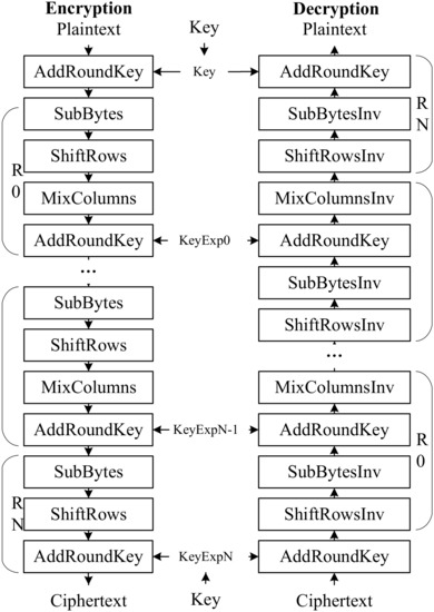
Figure 1.
AES-128 encryption and decryption process.
2.2. ECC Protocols
Figure 2 illustrates the ECC algorithm structure, which can be divided into the modular computing layer, the elliptic curve arithmetic layer, and the protocol layer.
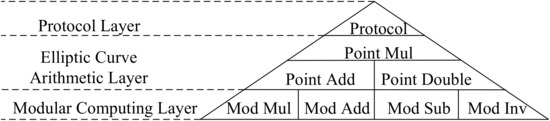
Figure 2.
ECC algorithm structure.
The modular computing layer constitutes the basic operations including modular multiplication(Mod Mul), modular add/sub(Mod Add/Sub) and modular inversion(Mod Inv) of binary field . The NIST-recommended binary fields of ECC include , , , and , and are most commonly used. A longer bit width leads to a stronger safety level, but the difficulty and complexity of the basic calculations also increase exponentially. In practice, the binary field of ECC needs to be traded off according to encryption speed requirements and safety level requirements.
The elliptic curve arithmetic layer includes point addition, point doubling, and point multiplication on the elliptic curve. Point multiplication is a combination of point addition and point doubling, each of which is a combination of the basic modular operations in the modular computing layer. Due to the difficulty of the elliptic curve discrete logarithm problem, the complexity of the elliptic curve PM reverse solution is much greater than the complexity of the forward solution. Based on this nature, asymmetric private-public key pairs can be generated, ensuring the security and reliability of keys.
Eventually, various ECC protocols can be accomplished by point operations in the elliptic curve arithmetic layer. The majority of these protocols include Elliptic Curve Diffie–Hellman Keyma Exchange (ECDH), the Elliptic Curve Digital Signature Algorithm (ECDSA), etc. This design implements the ECDH-based encryption algorithm and ECDSA algorithm, which are described separately.
2.2.1. ECDH-Based Encryption Algorithm
Figure 3 illustrates the overall flow of the ECDH-based encryption and decryption algorithm. Only the public key, ciphertext, and curve information are passed through the channel. Even if the eavesdroppers launch an attack, the plaintext cannot be obtained without the private key. This is a full reflection of the security advantages of asymmetric keys.
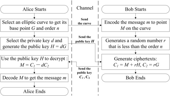
Figure 3.
ECDH-based encryption and decryption process.
ECDH is a key exchange protocol performed on elliptic curves. Suppose that two people, Alice and Bob, wish to exchange a secret key with each other. Alice generates a private key and a public key (where G is the base point of the curve). If Alice send the public key to Bob, he can obtain with his private key . Similarly, if Bob sends the public key , Alice can obtain point . Because , Alice and Bob can obtain the same information using ECDH. Therefore if valuable secret information is encrypted by the calculated points and , any eavesdropper would only have access to the public key and the base point in the channel, which are not sufficient to obtain the real encryption key of the shared secret information.
To take this one step further, if the secret data are involved in the ECDH process, ECDH-based data encryption can be achieved. Suppose that two people, Alice and Bob, wish to exchange secret data with each other. Alice has a private key d and sends the public key H over the channel to Bob. Bob maps the plaintext m to a point on the elliptic curve using plaintext embedding. After that, Bob selects a random number r less than the order n as his private key, and calculates the point and , corresponding to the shared secret information S and the public key in the ECDH algorithm. In this way, the plaintext is mixed into shared secret information by a point addition. Finally, Bob uses and as ciphertexts and sends them back to Alice to complete the data encryption.
The ECDH-based decryption algorithm works in the following way: Alice uses her private key and the received ciphertext to calculate . Substitute the formulas , , and into to obtain:
Therefore, calculating can help to find Bob’s plaintext embedding point M and then recover the plaintext m to complete decryption.
2.2.2. ECDSA
ECDSA uses elliptic curves to create a signature on the data. The signature ensures that the message content has not been tampered with by a third party. Anyone can verify its authenticity without compromising security.
Figure 4 illustrates the overall process of the ECDSA signature and verification, which only passes the public key and signature in the channel, ensuring the privacy of the private key.
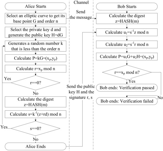
Figure 4.
ECDSA process.
To create an ECDSA signature, the sender of the message, Alice, will perform the following steps:
- Select a random number k, complete PM to obtain the point and the x coordinate of P;
- Calculate the first non-zero signature value ;
- Perform a HASH operation on the message m to obtain its digest value z;
- Calculate the second non-zero signature value ;
- Send the public key H, message m and signature to Bob.
To verify an ECDSA signature, the recipient, Bob, will perform the following steps:
- Perform a HASH operation on the message m to obtain its digest value z;
- Calculate and ;
- Calculate ;
- Compare the x coordinate value of P with the signature r. If they are equal, the verification is passed. If they are not equal, the verification fails.
The principle of the ECDSA verification can be deduced by expanding the P:
Substitute into the formula of P, and the following formula can be obtained:
From the deduction above, it is clear that the P in the signature stage and the P in the verification stage are the same points obtained through different calculation methods. Therefore, whether is established can determine whether the ECDSA verification is passed.
2.3. SRAM PUF Soft-Decision Algorithm
The SRAM power-on value is unique due to random differences caused by process deviations during manufacturing. Based on this principle, SRAM PUF uses the SRAM initial value to build PUF and achieves the chip authentication function.
SRAM PUF is sensitive to noise. Ambient noise can reverse some SRAM units that are not strongly biased toward “1” or “0”, so the initial value of SRAM is different at each power-on. SRAM tests were carried out in [41,42] at different temperatures, which led to the conclusion that the probability of error is between 3% and 15%. As the temperature decreases, the probability of error may be higher. However, when SRAM PUF is used as a chip key or for identity authentication, a fixed value must be guaranteed for each power-on. Therefore, error correction codes are used to correct the initial SRAM power-on value and solve the problem of unstable SRAM PUF output. Bosch completed SRAM PUF error correction on hardware for the first time with the Helper Data Algorithm (HDA) [43]. The principle of HDA is to use helper data to map the SRAM PUF to a codeword of the error correction code. Moreover, HDA can ensure that the helper data do not cause SRAM PUF information leakage.
It is stated in [44] that the error of each bit in SRAM is not entirely random. Most of the bits are very stable, and the power-on value of only some bits changes frequently. Therefore, HDA usually uses a soft-decision method. The principle of soft-decision HDA is to sample the data multiple times and record the error probability of each bit. The error correction code can work more efficiently and generate more accurate results by considering the error probability [44,45]. For SRAM, error probability can be easily obtained by simply powering on and counting repeatedly, which makes soft-decision HDA very practical. The specific algorithm of soft-decision HDA is as follows, which is divided into an enrollment stage and a recovery stage, as shown in Figure 5.

Figure 5.
HDA soft-decision process.
Enrollment stage: Select an SRAM initial value y as the standard value, which is the target value to be corrected during the recovery stage. Repeat the SRAM power-on 100 times and record the error probabilities of each bit between the initial value of each time and y. Then, randomly select a codeword c of Reed–Muller code, calculate the helper data , and save w, P to FLASH. Since P is the probability of an error occurring between each SRAM value, it is impossible to determine whether a particular bit is “1” or “0”, so P does not affect the overall security. The statistical process of P and the writing process of w and P should be performed at manufacturing.
Recovery stage: After the chip is delivered to the user, a random SRAM initial value is obtained during each power-on. Due to the initial value bit error rate, the SRAM initial value is different from y. Calculate , and the result is an RM codeword with an error. Use P and for RM soft-decision error correction to obtain the correct code word c. The P provides more information for the RM code, thereby improving the error correction ability. After the error correction is complete, the correct PUF value can be calculated.
3. Optimization and Application of Cryptographic Algorithms Based on Image Real-Time Acquisition Chips
For modern high-resolution real-time images, the data throughput is enormous. For example, in the image processing of 5 RGB888 consecutive images per second with a resolution of 4K, the throughput is as high as 132.7 MB/s. The JPEG algorithm’s image throughput with a 50% compression ratio is also as high as 66.4 MB/s. To support this throughput on a digital circuit with a clock frequency of 500 MHz, the encryption rate requirement is as high as bits per cycle. Symmetric encryption algorithms operate faster than asymmetric encryption algorithms and can meet the requirement of such data throughput. The hardware design of AES-128 can complete encryption every ten cycles [46], which can be seen as a processing speed of bits per cycle, meeting the encryption rate requirement of bits per cycle and leaving enough of a margin. On the contrary, even the fastest ECC hardware implementation requires thousands of cycles to complete encryption on [17], which can be seen as less than 0.1 bits per cycle, and is far from meeting the speed requirement of real-time image encryption. Therefore, the symmetric encryption algorithm AES is a better choice in a real-time image encryption scenario. However, there is a risk of exposure to AES private keys during transmission. Once the key is intercepted by an attacker, the security of the entire chip is under threat. Therefore a solution to increase the security level of AES is necessary. In this design, the asymmetric algorithm ECC is used to encrypt the AES private key to solve this problem. To further guarantee the safety of the entire high-speed hardware design, the secure chip authentication PUF algorithm is also required to prevent chip cloning.
In summary, this section provided the algorithm base of a triple-hybrid encryption system with the combinations of AES, ECC, and PUF. In addition, these three classic encryption algorithms are optimized according to the image real-time acquisition chip scenario to increase safety performance, calculation speed, and resource utilization. The proposed optimized algorithms include modified AES with private key encryption by ECC, a modified AES-based pseudo-random number generator (PRNG), ECC PM optimization, custom ECDSA algorithm, and a fast ECDSA-PUF algorithm. In the following subsection, the triple-hybrid encryption system is introduced first. Afterward, the principle and function of each optimized algorithm in the triple-hybrid encryption system are introduced in detail.
3.1. Proposed Triple-Hybrid Encryption System Based on Image Encryption
Figure 6 illustrates the proposed original triple-hybrid encryption system. The encryption system has three layers. The top application layer based on ECC and AES algorithms is responsible for image data encryption. The bottom application layer is responsible for hardware authorization by using the ECC algorithm. The developer layer is responsible for generating PUF and it involves ECC and PUF algorithms. The details of the three layers of the encryption system are introduced in the following parts. Figure 7 illustrates the overall flow.
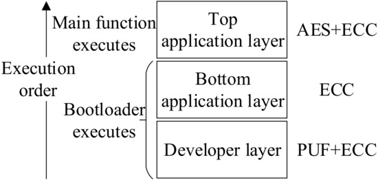
Figure 6.
Triple-hybrid encryption system structure.
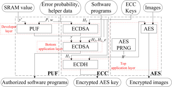
Figure 7.
Triple-hybrid encryption system flow.
The top application layer uses the ECDH algorithm to encrypt the AES private key, which is then used to encrypt image data. The specific steps are as follows:
- The user saves an ECC private key in the host computer, which then generates an ECC public key and sends it to the real-time image acquisition chip.
- The image real-time acquisition chip uses a modified AES-based PRNG hardware which consists of one LSFR and two AES to generate a random number W as the private key of the AES used to encrypt image data. The AES private key and the received public key undergo ECDH-based encryption, and the results are sent back to the host computer.
- After receiving the “ECDH-encrypted AES private key” and “AES encrypted image data”, the host computer uses the ECC private key to decrypt the AES private key, which is then used to decrypt the image data.
- If the users want to update the AES private key, the image real-time acquisition chip repeats step 2. A new pair of “AES private key cipher after ECDH encryption and AES encrypted image datum” is obtained and the host computer reads the new pair of datum for decryption.
The bottom application layer is used to authorize hardware and prevent attackers from using unauthorized hardware. {Program, PUF value y} (concatenate Program and y) are verified by custom-ECDSA to prove that the hardware belongs to authorized users, an original algorithm proposed in this paper. Only when the custom-ECDSA verification is passed can the software program jump to the main function flow. Otherwise, the CPU will not be able to run the software program. The hardware authorization process is divided into the user enrollment stage and the user activation stage.
At the user enrollment stage, the authorization of the hardware has not been completed. The developer holds the private key and users cannot obtain it. The custom ECDSA verification uses the solidified public key , so only the developer can make the program pass the verification and enter the main function. To authorize users, the developer assigns a pair of key and to users and write to the one-time programmable (OTP) device. At the user activation stage, the authorized user signs {Program, y} with provided by the developer. The hardware verifies the {Program, y} with , which has been solidified in the OTP device. Passing the verification indicates that the program is valid and proves that the current user has been authorized.
In the bottom application layer, we proposed an innovative application of PUF technology. Since the PUF value is used as a part of the message, the same software program and signature cannot be successfully verified on different chips due to changes in the PUF value, which further prevents unauthorized attackers from using the chip. If an attacker steals an authorized user’s software program and signature, the software program will still not execute properly on another unauthorized hardware.
The developer layer uses fast ECDSA-PUF, an originally proposed algorithm, to prevent an attacker from tampering with the PUF to pass the custom ECDSA of the bottom application layer. The developer signs the error probability P and the helper data w with an ECC private key . The hardware uses public key in the ROM to verify P and w. If the verification is passed, the PUF value y is valid.
In summary, the triple-hybrid encryption system mixes AES, ECC, and PUF algorithms. In terms of performance, the chip executes the bottom application layer and developer layer only once in the software bootloader. After that, the chip repeatedly performs the image encryption requests at the top application layer. The encryption system does not reduce the efficiency due to the multi-level algorithm, which ensures the system’s performance. In terms of security, each layer of the system is interconnected. As shown in Figure 8, problems at the upper layer are resolved in the lower layers. The failure of any link in the system will lead to authentication failure of the entire system, which significantly increases the difficulty of attacking and improves the system security.
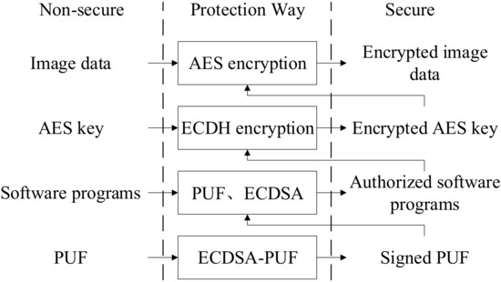
Figure 8.
Triple-hybrid encryption system protection relationship.
In the following subsections, the principles of each optimized algorithm used in the triple-hybrid encryption system are introduced sequentially.
3.2. AES Optimization and Application
3.2.1. AES Key Encryption
To solve the security problem of AES key, it is common practice to encrypt this key with an asymmetric encryption algorithm [32]. The novelty in this paper lies in the slow ECDH encryption used to encrypt the key. Since the slow process will only execute once in AES key encryption and once in AES key decryption, while the data encryption and decryption use the fast AES algorithm, the security problem is solved without dragging down the data processing speed.
3.2.2. Modified AES-Based PRNG
Since PRNG is used to generate AES keys in the triple-hybrid encryption system, it is essential to pay attention to the security of PRNG. PRNG needs to be practical and lightweight. The Linear Feedback Shift Register (LFSR) has a minor hardware overhead and is widely used to generate random numbers. However, Meier and Staffelbach proposed a rapidly related attack method for LFSR [47], which reduced the time complexity of cracking LFSR to . Todo optimized the rapid correlation attack method to achieve a more effective attack on LFSR [48]. Therefore, using the output of LFSR as the key of the cryptography system poses a great threat.
To further protect LFSR, an AES-based PRNG is proposed, based on the research result of [49], which states that random numbers will have sufficient redundancy after two AES encryption processes and cannot be inferred. Figure 9 illustrates the proposed AES-based PRNG. LFSR generates two different random numbers from two different cycles, one is used as the plaintext of the first AES, and the other is used as the key of the first AES. The first AES generates two ciphertexts from two cycles, which are used as the plaintext and the key of the second AES. Eventually, the ciphertext output of the second AES is the secure random number. Since an AES module already exists in the AES key encryption circuit, that AES module can be re-used in this AES-based PRNG encryption when that part is idle. In this way, the reliability of the random generator is greatly increased without adding additional hardware overhead.
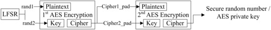
Figure 9.
AES-based PRNG.
3.3. ECC Optimization and Application
Since the ECC in our design does not affect the system encryption speed, its design purpose is more cost-dominant. As a result, ECC is implemented on the binary field , which has the lowest bit-width and thus lowest complexity in all NIST-recommended binary field ECC. Since the difficulty of cracking ECC on is still much bigger than cracking AES, such selection will reduce the hardware yield, but will not affect the system’s safety.
Since modular inversion operation is one of the most complex and resource-consuming operations in ECC, and no projected coordinate system can avoid it, this paper proposes a new method that completely removes modular inversion calculations in ECDSA hardware. The proposed method is custom ECDSA, which modifies some ECDSA steps while ensuring safety. The ECDSA protocol can be modified because both the sender and receiver of ECDSA in a triple-hybrid encryption system are the hardware owners. The local-based protocol does not need to agree with the receiver in the open channel so that the protocol can be customized. Furthermore, the proposed protocol customization method is non-public, which also increases the difficulty of cracking.
Custom ECDSA removes two modular inversions in the protocol. Figure 10 illustrates the process of custom ECDSA, where Alice is the host computer and Bob is the chip. The first modular inversion to be removed is the calculation of in ECDSA verification when the projected coordinate system is restored to the affine coordinate system. The custom ECDSA protocol verifies whether is equal to X ( are the projected coordinate values of the point P) instead of whether is equal to r. The second modular inversion to be removed is the calculation of in the ECDSA signature formula. In the triple-hybrid encryption system, the image real-time acquisition chip only needs to perform the verification, and the signature is completed on the host computer. Therefore, can be calculated in advance on the host computer, and then sent to the chip and saved as a signature. Similarly, can also be pre-calculated on the host and sent to the chip. Based on the improvements above, the optimized verification no more has modular inversion operation, which reduces the overhead of the image real-time acquisition chip and improves the speed.
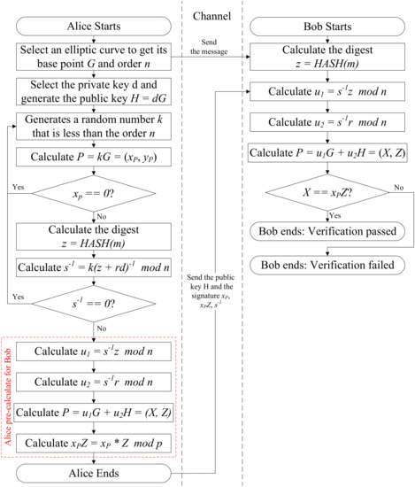
Figure 10.
Custom ECDSA process.
3.4. SRAM PUF Optimization and Application
3.4.1. Risks of SRAM PUF
SRAM PUF soft-decision is based on the premise that SRAM is secure and invisible outside the chip. However, SRAM is directly connected to the CPU in the image real-time acquisition chip. Attackers can read it using software or even probes or SEM for invaded forced reads. Once the attacker reads the SRAM, is fetched. The attacker then uses the same method to read FLASH to obtain w and P and calculates with . Finally the attacker obtains all SRAM PUF-related data y, , c. Since the soft-decision algorithm adds P, the attacker can modify P to indirectly control the corrected c to modify y, achieving the effect of cloning PUF.
3.4.2. Optimized Fast ECDSA-PUF
The triple-hybrid encryption system proposes an ECDSA-based soft-decision SRAM PUF (ECDSA-PUF) algorithm, which signs the helper data w and the error probability P with ECDSA. SRAM PUF must perform ECDSA verification on w and P before each generation. Under the protection of ECDSA, even if an attacker modifies w and P in FLASH, it is impossible to generate a valid ECDSA signature and verify SRAM PUF successfully. In this way, a cloning attack is prevented.
Figure 11 illustrates the optimized fast ECDSA-PUF algorithm. The fast ECDSA-PUF algorithm reuses the custom ECDSA already in the triple-hybrid encryption system, so only a small area increment is induced. As for speed, since some steps in custom ECDSA are moved to the enrollment stage which is calculated before leaving the factory, the computation time it takes in the recovery stage on the chip is shorter than normal ECDSA. Therefore, integrating custom ECDSA in PUF greatly increases the safety level of SRAM PUF, at the price of a little more boot time, which is bearable.
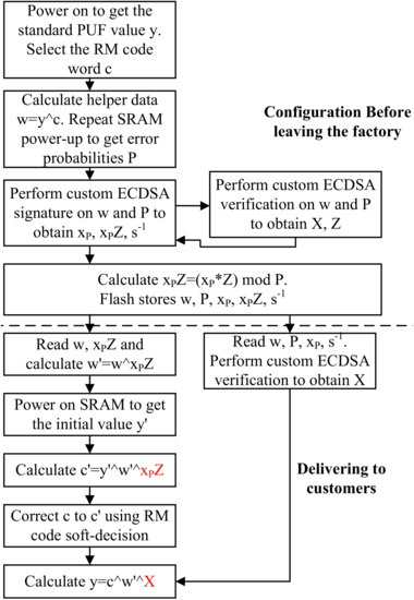
Figure 11.
Optimized fast ECDSA-PUF process.
Since the custom ECDSA verification in ECDSA-PUF uses the result whether X is equal to , such a single-bit signal is vulnerable to direct attack and modification in the circuit layout, which will thereby modify the correctness of the entire ECDSA-PUF. In order to solve this problem, the ECDSA-PUF adds X and in different places of the algorithm’s formula, as highlighted in red in Figure 11. If , two XOR will be eliminated, and the correct PUF value can eventually be obtained. This optimization method can improve the overall complexity and safety level without adding redundant circuits.
4. Design and Implementation of Proposed Image Encryption Subsystem
In this section, the implementation of an image encryption subsystem based on the proposed triple-hybrid encryption system is discussed in detail. The subsystem includes the hardware implementations of all optimized cryptographic algorithms mentioned before, to provide the crucial high-speed and secure encryption function for the real-time image acquisition chip. In addition, the ASIC and FPGA implementation results of this subsystem are compared with other mainstream designs.
4.1. Subsystem Overall Structure
Figure 12 illustrates the overall structure of the image encryption subsystem. On the left side lies the bus communication part in charge of communicating control signals and data with other subsystems. The CPU outside the subsystem can use software to access APB and AHB buses, and configure the public key and base point of ECDH, the public key, base point, signature, and message of ECDSA. The ECDH ciphertext and ECDSA verification results can also be read through these buses. The data that users need to write or read through APB and AHB buses are all in the application layer of the triple-hybrid encryption system. Other data, including AES keys, encrypted random numbers, image data before encryption, and SRAM PUF values, is entirely controlled by hardware and cannot be accessed by software methods, ensuring the security of the image encryption subsystem.
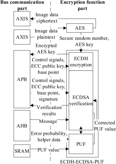
Figure 12.
Image encryption subsystem overall structure.
The core of the design is the encryption function part on the right side of Figure 12, which covers AES encryption, ECDH encryption, custom ECDSA, fast ECDSA-PUF, and AES PRNG. As these algorithms share the same basic operations of modular computations, only one set of basic modular computations hardware is implemented and then scheduled by the top-level control to avoid simultaneous invocation and maximize its utilization. Other details of AES and ECDH-ECDSA-PUF modules will be described separately in the following subsections.
4.2. Hardware Design of AES Module
Different from other designs, the structure of AES in this work is optimized for the modified AES-PRNG mentioned in Section 3.2.2 as shown in Figure 13. Figure 14 illustrates the whole AES data flow, where the red AES part is multiplexed. In the hardware circuit, the design utilizes the idle time of AES data encryption and multiplexes the AES module to protect the PRNG. Outputting the LFSR to the AES encryption module adds sufficient redundancy to complete the implementation of a secure PRNG. The generated secure random number is used as the AES key for image encryption and the plaintext to be encrypted by the ECDH module.
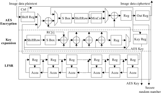
Figure 13.
AES module structure.
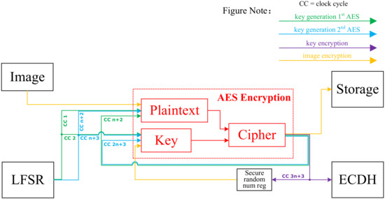
Figure 14.
AES data flow.
4.3. Hardware Design of ECDH-ECDSA-PUF Module
4.3.1. Module Reuse Strategy
As ECC and PUF modules are not emphasized on computation speed in the triple-hybrid encryption system, the hardware structure design of the ECDH-ECDSA-PUF algorithm is mainly aimed at hardware reuse and speed matching.
The first multiplex technique is that the fast ECDSA-PUF algorithm and custom ECDSA verification algorithm share the same ECDSA verification module, which is shown in Figure 15. Figure 16 is the data flow that illustrates how the same ECDSA hardware module is shared by two different processes in different stages. When the system calculates the fast ECDSA-PUF process, the ECDSA verification module needs to verify the helper data, error probability, and signature saved in FLASH, and the PUF module is responsible for executing the soft-decision HDA algorithm. When the system calculates the custom ECDSA process, the ECDSA verification module needs to verify the message and signature from APB and AHB buses.
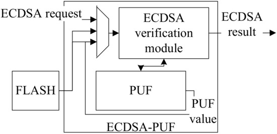
Figure 15.
Fast ECDSA-PUF and custom ECDSA shares the same ECDSA verification module.
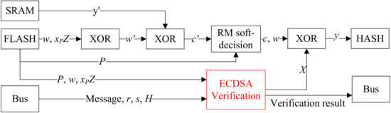
Figure 16.
Fast ECDSA-PUF and custom ECDSA data flow.
The second multiplex technique is that the ECC point operation module is shared by a custom ECDSA verification process and ECDH encryption process. Figure 17 illustrates their data flow, where the red point operation part is multiplexed. The two processes are designed to reuse the same ECC point operating hardware module to make a lightweight system.
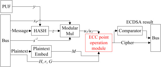
Figure 17.
Custom ECDSA and ECDH data flow.
4.3.2. PUF Structure
Figure 18 illustrates the PUF module structure, which is divided into a helper data part and a RM soft-decision part. The helper data part mainly contains XOR gates, corresponding to the three XOR calculations in the recovery stage of the fast ECDSA-PUF algorithm. RM soft-decision part includes RM code recursion logics, an address generator, and a RM code ALU. The address generator can generate SRAM read and write addresses based on recursive logic. ALU is used to calculate the operation of RM code decoding. In this design, the data path is optimized as a pipeline design, the SRAM read is performed in advance before the next ALU calculation, and the SRAM write is performed in parallel during the current ALU calculation. There is no stall in hardware computing, which improves the utilization of hardware.
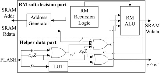
Figure 18.
PUF module structure.
4.3.3. ECDSA and ECDH Structure
The scheduling of basic point and modular operations in ECC protocol and ECC PM takes on a step-by-step sequential feature, so PM and upper-level protocol can be implemented by software methods. This work adopts the design method of [50] which designed the CPU-like hardware structure of “instruction ROM + RAM + ALU”. While the structure in [50] is only built for the PM layer, this design modified it to the ECDH and ECDSA layer to further reduce the resource overhead of the ECC-related module.
Figure 19 illustrates the modified “instruction ROM + RAM + ALU” structure of the ECDH encryption module and the ECDSA verification module. Both modules share the same point operation module as a shared public region and use a multiplexer to distribute control signals. The modular multiplication and HASH modules are exclusive parts of the ECDSA verification module. The plaintext embedding algorithm is an exclusive part of the ECDH encryption module. In the “instruction ROM + RAM + ALU” structure, the control signals of the ECDH encryption algorithm and the custom ECDSA verification algorithm are solidified and saved in instruction ROMs. The two algorithms have two corresponding instruction ROMs which can be selected by the switching signal. RAM caches all variables and changes the address according to the control signal in the instruction ROMs, and the write data is selected according to multiplexers. ALU supports basic functions of modular multiplication, modular addition, and modular square on binary field. The calculation type is controlled according to the instruction ROM, and the result can be output outside the module or written back to RAM to realize point operations including point multiplication, point addition, and point doubling. All data is written to RAM uniformly and dispatched by RAM address, reducing the logic circuit overhead of the data path.
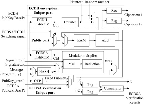
Figure 19.
ECDH encryption module and ECDSA verification module structure.
4.4. Implementation Results and Comparisons
The ASIC implementation results of the image encryption subsystem proposed in this chapter come from the final chip solution, an image acquisition chip manufactured in SMIC nm process. In addition to the ASIC implementation, the image encryption subsystem is also implemented on the FPGA platform to verify the subsystem more fairly compared with other works, especially works focusing on AES and ECC. To ensure equity, result comparisons of FPGA implementation should use the same series of FPGA. There is no guarantee of fairness in ASIC comparison because the performance of the same circuit varies greatly on a different process, voltage, and temperature. Therefore, only the PUF algorithm which is strictly related to hardware and cannot be reliably verified by FPGA should be compared with other literature using ASIC results.
4.4.1. FPGA and ASIC Implementation Results
ASIC results are synthesized on SMIC 40 nm library by Synopsys Design Compiler synthesis tool. The maximum clock frequency of the subsystem can reach 480 MHz, and the total area is 94,812.4 m. Note that this result is before Place and Route (P&R). Table 1 shows the resource usage results of each module, where the gate equivalent (GE) is calculated as the total area divided by one NAND2 gate area under the corresponding process [51,52]. According to the area results, the ECDH encryption module and the ECDSA verification module accounted for 67.8% of the total subsystem area with 89,518.1 GE. If the module multiplexing design were not adopted, the hardware resource usage of the two modules would have been doubled, leading to approximately 60% more area in the entire system. The area of the PUF module is comparable to the AES module, with only 21,966.8 GE, which can fully reflect the lightweight of the SRAM PUF algorithm. Because of module multiplexing, the ECDSA-PUF algorithm does not add additional resources to the PUF module to realize the ECDSA algorithm in it.

Table 1.
Image encryption subsystem resource usage results under ASIC implementation.
At the maximum frequency, Table 2 shows the calculation speed of each algorithm on ASIC. The time to generate PUF is equal to 100.8 s, which is counted as part of the bootloader time. An additional 100.8 s boot time is considered acceptable for normal users. The other speed-emphasized algorithm, AES, has a computation time of 0.02083 s, which can achieve a peak encryption speed of 6.15 Gb/s with uninterrupted input. This speed performance can fully meet the requirements of real-time encryption of high-resolution and high-frame-rate images.
Table 2.
Image encryption subsystem speed results under ASIC implementation.
As for FPGA results, the Synplify Premier synthesizer is used for implementations on Xilinx Virtex-5 and Virtex-7 devices. Table 3 shows the area results implemented on the two FPGA devices. The clock frequency of the image encryption subsystem can reach 132.5 MHz on Virtex-5, and 137.6 MHz on Virtex-7. Table 4 shows the calculation time of AES, ECC, and PUF based on the two devices. The area ratio of each module and the speed ratio of the algorithm implemented by FPGA are basically the same as those implemented by ASIC.
Table 3.
Image encryption subsystem resource usage results under FPGA implementation.
Table 4.
Image encryption subsystem speed results under FPGA implementation.
4.4.2. FPGA Result Comparisons of AES and ECC
Table 5 shows the comparison results of the AES FPGA implementation with other works. Since works on the hardware implementation of AES may either choose the “full-pipeline design” idea or the “multi-cycle design” idea, comparisons between designs with different biases are meaningless. Therefore, the reference works we chose to list in Table 5 are all “multi-cycle design”. In order to better evaluate the trade-off between area and speed of each design, the formula (4) is used to calculate performance [53]. The higher the performance, the more cost-effective the design.
Table 5.
AES implementation results comparison.
Table 5 shows that although the throughput of the proposed AES design is the lowest of all designs, the implementation area is the smallest. This is because the proposed design cares about the image encryption speed but does not blindly aim at the extreme speed. The number of hardware resources is significantly reduced. It is 60.1% smaller than the design of [55], which uses the least amount of resources among all literature. Thanks to the reduced hardware area and sufficient throughput, the design in this paper has the highest performance among all Virtex-7 implementations. Among all the Virtex-5 implementations, refs. [53,57] use a “partial-pipeline design”, which improves throughput at the cost of area. Their performance is higher than the proposed design, but considering that the AES of the proposed design is also used for the PRNG and shares the clock frequency limit of other modules such as ECC, the performance under Virtex-5 is still acceptable. It can then be concluded that the AES resource usage of this design is at the top level, and the AES performance is relatively high.
Table 6 shows the result comparison of the ECC algorithm. This ECC implementation is a custom design, which is to adapt to the entire encryption system, not simply to optimize area or speed. Therefore, from the comparison of Table 6, it can be concluded that the hardware resource area of this design is the lowest. Compared with the lowest area literature [18], the proposed hardware resource is reduced by 43.4%. This is because the proposed hardware reduces the width of the multiplier, saving a lot of multiplier hardware area. Moreover, although the ECC implementation of this design is inferior to the other designs in terms of speed, its speed is sufficient for encrypting the AES key and will not drag down the system encryption speed. On the other hand, the reduction in hardware area and power consumption at the expense of speed loss contributes greatly to the whole system.
Table 6.
ECC implementation results comparison.
4.4.3. ASIC Result Comparisons of PUF
The hardware implementation result of the fast ECDSA-PUF algorithm is compared with that of other works on SRAM PUFs. The comparison of SRAM PUF mainly aims at lower BER (bit error rate) and GE (gate equivalent) per bit. BER is to measure the PUF stability. GE per bit reflects the consumption of hardware resources excluding the influence of the PUF length. GE per bit can be calculated by formula (5) [62]. In fact, the parameter of BER and GE per bit has little to do with the process, therefore implementations of different processes can be compared as shown in Table 7.
It can be obtained from Table 7 that the number of GE per bit in this paper is at the middle level. However, refs. [63,64], which have less GE per bit, are worse in terms of BER. The BER of [63,64] is too high, which may affect the normal functioning of the chip.
Table 7.
PUF implementation results comparison.
Table 7.
PUF implementation results comparison.
| Works | ASIC Process (nm) | Area per bit (m/bit) | GE per bit (GE/bit) | BER |
|---|---|---|---|---|
| [62] | 65 | 49.12 | 25.58 | 2.7 × 10 |
| [63] | 14 | 1.84 | 11.83 | 1.45 × 10 |
| [65] | 65 | 50.7 | 26.40 | 1.56 × 10 |
| [64] | 65 | 17.9 | 9.32 | 2.5 × 10 |
| This work | 40 | 15.40 | 21.45 | 3 × 10 |
Moreover, the ECDSA-PUF hardware of this paper can increase the SRAM PUF bit number by multiplexing the ECDSA-PUF module and repeating the custom ECDSA and soft-decision HDA calculation. Therefore, in other application scenarios that require higher information entropy, GE per bit of the structure used in this design will decrease exponentially, as is shown in Figure 20. This is an unachievable effect on other related works, proving that the proposed design is more advanced in terms of lightweight. The SRAM PUF proposed by [62] is very advanced in BER. The fast ECDSA-PUF proposed in this paper pays more attention to speed, security, and lightweight, so an error correction code with a lower BER is chosen, but it is still sufficient for the current BER requirement.
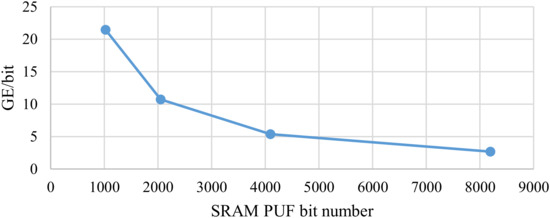
Figure 20.
Relationship between PUF bit number and GE per bit in this design.
In summary, the implementation results of AES, ECC and PUF prove that the three proposed algorithms have been reasonably optimized for the requirements, and the speed and area of the triple-hybrid encryption system hardware are not affected by the algorithm mixture.
5. Real-Time Image Acquisition SoC Based on Triple-Hybrid Encryption System
In order to realize a complete application of the image encryption subsystem, this section illustrates the integration of the subsystem into a real-time image acquisition SoC. The SoC implements an application example that captures one 4208 × 3120 RAW10 image per second and completes real-time encryption and storage.
5.1. SoC Hardware Structure
Figure 21 illustrates the subsystem connection relationship in SoC hardware. The image encryption subsystem is the core system to ensure the system’s security. The input of the image encryption subsystem is an image acquisition subsystem that collects and transmits image data. And its encrypted output is stored in a storage subsystem. These three subsystems together form the data path of the image data. In order to control and schedule the three subsystems, the SoC has added software control and bus subsystem to provide software program functions for the whole system. The software program only controls the scheduling of hardware and does not really participate in image data processing, encryption, and calculation, which are all done by hardware modules. In order to reduce the power consumption of SoC, an asynchronous clock subsystem is added to turn on the clock of each module only when it is active. Image encryption subsystem, image acquisition subsystem, storage subsystem, software control, bus subsystem, and asynchronous clock subsystem constitute a real-time image acquisition SoC based on the triple-hybrid encryption system.
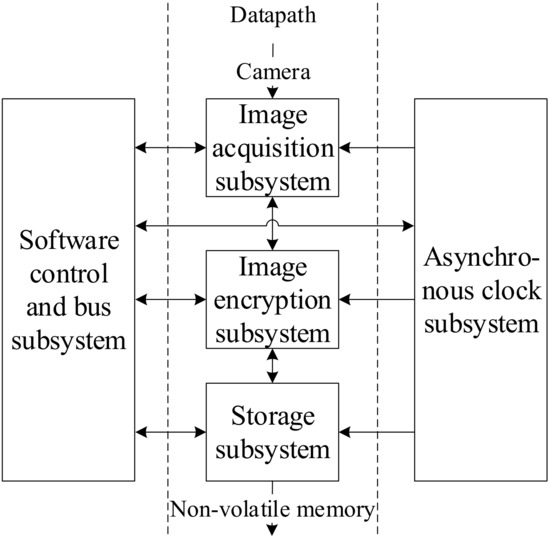
Figure 21.
Connection relationship in SoC structure.
Figure 22 shows the detailed structure of the SoC. In the software control and bus subsystem, since all data processing in the chip is completed by hardware and the software only needs to read and write registers for subsystem scheduling, there is no demand for CPU for complex computing ability. Therefore, this design uses ARM Cortex-M0+ CPU, a lightweight CPU for embedded chips suitable for this design. In the image acquisition subsystem, the image data is streamed to the image encryption subsystem through the data path of “MIPI Controller-ISP-JPEG”. AXIS bus is used and the highest clock frequency is allocated as the image data transmission of the MIPI controller, ISP module, and JPEG compression module is the path that requires the highest transmission speed in the SoC. In the storage subsystem, three types of non-volatile storage devices are designed: (1) NAND FLASH in the chip package; (2) External pluggable SD card; (3) Transfer to the host computer via USB. Diversified storage methods allow the SoC to meet different target requirements.
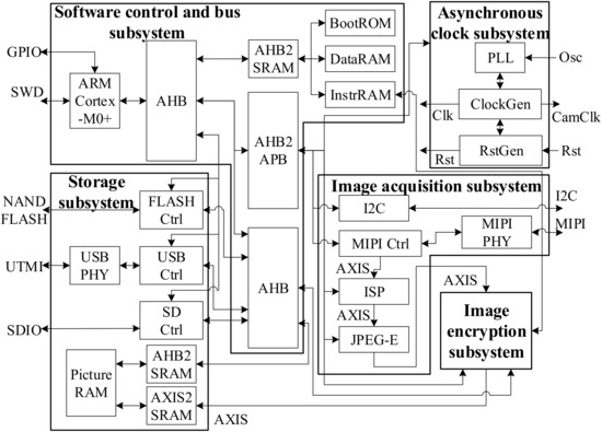
Figure 22.
SoC detailed structure.
5.2. SoC Software Programs
With the help of software control and bus subsystems, the SoC can control each subsystem through a software program. The software program includes all the control and scheduling of subsystems and can be divided into two parts. The first part is the software for the bootloader, as exhibited in Figure 23. The second part is the software for the main function, as shown in Figure 24.
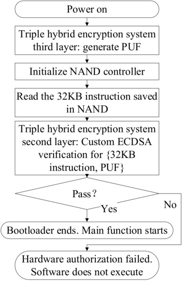
Figure 23.
SoC software bootloader.

Figure 24.
SoC software main function.
The bootloader program is invisible and is solidified by the boot ROM. To protect the bottom application layer and the developer layer as is mentioned in Section 3.1, the steps of generating PUF and program verification are placed in the bootloader so that users cannot bypass it, which strengthens the security of the chip.
The software program jumps to the main function part after bootloader loading is completed. The main function part includes the processes of the top application layer of the triple-hybrid encryption system and image acquisition, storage, and transmission required to cooperate with the top application layer. Since there are three storage modes, the main function selects the mode at the beginning and executes storage-subsystem-related programs according to the mode. The program then configures the asynchronous clock according to the current storage mode, configures all image-acquisition-related modules, and starts image acquisition. After that, the program adjusts the focus according to the current image’s clarity and performs JPEG compression after focusing. Finally, the JPEG image is output to the image encryption subsystem, and the software program enters the main loop and continues to work until the data is all processed.
5.3. Implementation Results
The image acquisition SoC based on the proposed triple-hybrid encryption system is implemented on ASIC. The results are synthesized by Synopsys Design Compiler synthesis tool based on SMIC 40 nm process library. All timing constraints of the SoC passed. The total area is 10,590,806 m 10.59 mm, and Table 8 shows the area consumption of each subsystem. The SoC is successfully placed and routed under the layout floorplan of 4 mm × 4 mm, and then delivered to the foundry to complete the tape out. The final back-end layout is shown in Figure 25.
Table 8.
Area of each subsystem in SoC.
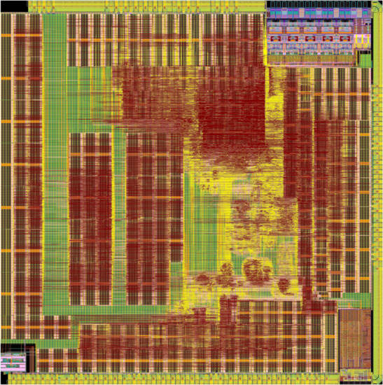
Figure 25.
SoC layout.
Figure 26 illustrates the actual workflow of the triple-hybrid encryption system on the implemented chip, together with the actual time required for each step. In Example 2, when a new batch of image data is ready to be encrypted, a new AES private key should be re-encrypted first. Although ECDH encryption accompanies each AES encryption, the time of ECDH encryption only accounts for 0.00475% and 0.00317% of each encryption time, respectively. In the two examples, the time from start to the {software program, PUF} verification step is the entire preparation time for each encryption flow. The additional boot time of 0.192 ms is barely noticeable by users, which only accounts for 0.00959% and 0.00383% of the total time, respectively. In field applications, as the amount of encrypted image data increases after each startup, the proportion of the preparation time will be lower, which fully reflects the advantage that the triple-hybrid encryption system will not slow down the software startup speed but will significantly improve the security of the whole chip.
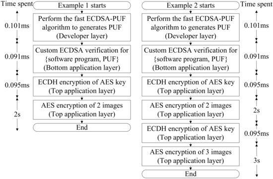
Figure 26.
Triple-hybrid encryption system actual workflow in the chip.
6. Conclusions
This paper proposes an original triple-hybrid encryption system for the requirements of real-time image acquisition chips. The proposed encryption system makes full use of the respective advantages of the three algorithms so that the real-time image acquisition chip can obtain sufficient security. The encryption system also provides a new idea for other designs with the exact security requirements. The improved algorithm and triple-hybrid encryption system are implemented in hardware and constitute an image encryption subsystem. Finally, the image encryption subsystem, image acquisition subsystem, storage subsystem, software control, and bus subsystem, and asynchronous clock subsystem form a real-time image acquisition SoC based on the triple-hybrid encryption system. In the age of information, high-speed cryptography technology will become an essential demand for future security development, and the demand for image security is bound to be higher. The research results presented above in this paper will contribute to the development of high-speed cryptography and image encryption applications.
Author Contributions
Conceptualization, J.L., Y.L. and W.G.; methodology, J.L., Y.L. and W.G.; software, Y.L.; validation, J.L. and W.G.; formal analysis, J.L.; investigation, J.L., Y.L. and W.G.; resources, W.G.; writing—original draft preparation, Y.L. and J.L.; writing—review and editing, J.L.; supervision, F.W. and W.G.; project administration, J.L.; funding acquisition, F.W. All authors have read and agreed to the published version of the manuscript.
Funding
This research was funded by National Key Technologies Research & Development Program grant number 2021YFC3001901.
Institutional Review Board Statement
Not applicable.
Informed Consent Statement
Not applicable.
Data Availability Statement
All data can be provided upon reasonable request to the corresponding author.
Conflicts of Interest
The authors declare no conflict of interest.
Abbreviations
The following abbreviations are used in this manuscript:
| AES | Advanced Encryption Standard |
| ECC | Elliptic Curve Cryptography |
| PUF | Physical Unclonable Function |
| SoC | System on Chip |
| NIST | National Institute of Standards and Technology |
| DES | Data Encryption Standard |
| RSA | Rivest, Shamir, Adleman |
| PM | Point Multiplication |
| ASIC | Application Specific Integrated Circuit |
| FPGA | Field Programmable Gate Array |
| LUT | Look Up Table |
| SEM | Scanning Electron Microscope |
| HDA | Helper Data Algorithm |
| ECDH | Elliptic Curve Diffie Hellman Key Exchange |
| ECDSA | Elliptic Curve Digital Signature Algorithm |
| RM | Reed-Muller Code |
| PRNG | Pseudorandom Random Number Generator |
| LFSR | Linear Feedback Shift Register |
| BER | Bit Error Ratio |
| OTP | One Time Programmable |
| ALU | Arithmetic&logical Unit |
| P&R | Place and Route |
| GE | Gate Equivalent |
References
- Arora, H.; Soni, G.K.; Kushwaha, R.K.; Prasoon, P. Digital Image Security Based on the Hybrid Model of Image Hiding and Encryption. In Proceedings of the 2021 6th International Conference on Communication and Electronics Systems (ICCES), Coimbatre, India, 8–10 July 2021; pp. 1153–1157. [Google Scholar]
- Matted, S.; Shankar, G.; Jain, B.B. Enhanced Image Security Using Stenography and Cryptography. In Computer Networks and Inventive Communication Technologies; Springer: Berlin/Heidelberg, Germany, 2021; pp. 1171–1182. [Google Scholar]
- Saxena, A.K.; Sinha, S.; Shukla, P. Design and development of image security technique by using cryptography and steganography: A combine approach. Int. J. Image Graph. Signal Process. 2018, 10, 13. [Google Scholar] [CrossRef]
- Al-Haj, A.; Abdel-Nabi, H. Digital image security based on data hiding and cryptography. In Proceedings of the 2017 3rd International Conference on Information Management (ICIM), Chengdu, China, 21–23 April 2017; pp. 437–440. [Google Scholar]
- Růžička, V.; Franchetti, F. Fast and accurate object detection in high resolution 4K and 8K video using GPUs. In Proceedings of the 2018 IEEE High Performance Extreme Computing Conference (HPEC), Waltham, MA, USA, 25–27 September 2018; pp. 1–7. [Google Scholar]
- Zhang, Q. An Overview and Analysis of Hybrid Encryption: The Combination of Symmetric Encryption and Asymmetric Encryption. In Proceedings of the 2021 2nd International Conference on Computing and Data Science (CDS), Stanford, CA, USA, 28–29 January 2021; pp. 616–622. [Google Scholar]
- Wang, P.; Zhang, Y.; Yang, J. Research and design of AES security processor model based on FPGA. Procedia Comput. Sci. 2018, 131, 249–254. [Google Scholar] [CrossRef]
- Gupta, K.; Silakari, S. Ecc over rsa for asymmetric encryption: A review. Int. J. Comput. Sci. Issues IJCSI 2011, 8, 370. [Google Scholar]
- Halak, B.; Zwolinski, M.; Mispan, M.S. Overview of PUF-based hardware security solutions for the Internet of Things. In Proceedings of the 2016 IEEE 59th International Midwest Symposium on Circuits and Systems (MWSCAS), Abu Dhabi, United Arab Emirates, 16–19 October 2016; pp. 1–4. [Google Scholar]
- Mall, P.; Amin, R.; Das, A.K.; Leung, M.T.; Choo, K.K.R. PUF-based authentication and key agreement protocols for IoT, WSNs and smart grids: A comprehensive survey. IEEE Internet Things J. 2022, 9, 8205–8228. [Google Scholar] [CrossRef]
- Kiyan, T.; Lohrke, H.; Boit, C. Comparative Assessment of Optical Techniques for Semi-Invasive SRAM Data Read-out on an MSP430 Microcontroller. In Proceedings of the ISTFA 2018 44th International Symposium for Testing and Failure Analysis, Phoenix, AZ, USA, 28 October–1 November 2018; ASM International: Phoenix, AZ, USA, 2018; p. 266. [Google Scholar]
- Faraj, M.; Gebotys, C. Quiescent photonics side channel analysis: Low cost SRAM readout attack. Cryptogr. Commun. 2021, 13, 363–376. [Google Scholar] [CrossRef]
- Gueron, S.; Mathew, S. Hardware implementation of AES using area-optimal polynomials for composite-field representation GF (2ˆ 4)ˆ 2 of GF (2ˆ 8). In Proceedings of the 2016 IEEE 23nd Symposium on Computer Arithmetic (ARITH), Silicon Valley, CA, USA, 10–13 July 2016; pp. 112–117. [Google Scholar]
- Ueno, R.; Morioka, S.; Miura, N.; Matsuda, K.; Nagata, M.; Bhasin, S.; Mathieu, Y.; Graba, T.; Danger, J.L.; Homma, N. High throughput/gate AES hardware architectures based on datapath compression. IEEE Trans. Comput. 2019, 69, 534–548. [Google Scholar] [CrossRef]
- Baby Chellam, M.; Natarajan, R. AES hardware accelerator on FPGA with improved throughput and resource efficiency. Arab. J. Sci. Eng. 2018, 43, 6873–6890. [Google Scholar] [CrossRef]
- Habek, M.; Gene, Y.; Aytas, N.; Akkoc, A.; Afacan, E.; Yazgan, E. Digital Image Encryption Using Elliptic Curve Cryptography: A Review. In Proceedings of the 2022 International Congress on Human-Computer Interaction, Optimization and Robotic Applications (HORA), Ankara, Turkey, 9–11 June 2022; pp. 1–8. [Google Scholar]
- Li, J.; Zhong, S.; Li, Z.; Cao, S.; Zhang, J.; Wang, W. Speed-Oriented Architecture for Binary Field Point Multiplication on Elliptic Curves. IEEE Access 2019, 7, 32048–32060. [Google Scholar] [CrossRef]
- Khan, Z.-U.-A.; Benaissa, M. Throughput/area-efficient ECC processor using Montgomery point multiplication on FPGA. IEEE Trans. Circuits Syst. II Express Briefs 2015, 62, 1078–1082. [Google Scholar]
- Van Dijk, M.; Rührmair, U. Protocol attacks on advanced PUF protocols and countermeasures. In Proceedings of the 2014 Design, Automation & Test in Europe Conference & Exhibition (DATE), Dresden, Germany, 24–28 March 2014; pp. 1–6. [Google Scholar]
- Rührmair, U.; van Dijk, M. PUFs in security protocols: Attack models and security evaluations. In Proceedings of the 2013 IEEE Symposium on Security and Privacy, Berkeley, CA, USA, 19–22 May 2013; pp. 286–300. [Google Scholar]
- Rührmair, U.; Jaeger, C.; Algasinger, M. An attack on PUF-based session key exchange and a hardware-based countermeasure: Erasable PUFs. In International Conference on Financial Cryptography and Data Security; Springer: Berlin/Heidelberg, Germany, 2011; pp. 190–204. [Google Scholar]
- Karakoyunlu, D.; Sunar, B. Differential template attacks on PUF enabled cryptographic devices. In Proceedings of the 2010 IEEE International Workshop on Information Forensics and Security, Seattle, WA, USA, 12–15 December 2010; pp. 1–6. [Google Scholar]
- Merli, D.; Schuster, D.; Stumpf, F.; Sigl, G. Side-channel analysis of PUFs and fuzzy extractors. In International Conference on Trust and Trustworthy Computing; Springer: Berlin/Heidelberg, Germany, 2011; pp. 33–47. [Google Scholar]
- Patterson, D.A.; Hennessy, J.L. Computer Organization and Design ARM Edition: The Hardware Software Interface; Morgan Kaufmann: Burlington, MA, USA, 2016. [Google Scholar]
- Lohrke, H.; Tajik, S.; Krachenfels, T.; Boit, C.; Seifert, J.P. Key extraction using thermal laser stimulation: A case study on xilinx ultrascale fpgas. IACR Trans. Cryptogr. Hardw. Embed. Syst. 2018, 573–595. [Google Scholar] [CrossRef]
- Singh, K.N.; Singh, A.K. Towards integrating image encryption with compression: A survey. ACM Trans. Multimed. Comput. Commun. Appl. TOMM 2022, 18, 1–21. [Google Scholar] [CrossRef]
- Rahimunnisa, K.; Karthigaikumar, P.; Christy, N.A.; Kumar, S.S.; Jayakumar, J. PSP: Parallel sub-pipelined architecture for high throughput AES on FPGA and ASIC. Cent. Eur. J. Comput. Sci. 2013, 3, 173–186. [Google Scholar] [CrossRef]
- Bağbaba, A.Ç.; Örs, B. Hardware implementation of novel image compression-encryption system on a FPGA. In Proceedings of the 2015 9th International Conference on Electrical and Electronics Engineering (ELECO), Bursa, Turkey, 26–28 November 2015; pp. 1159–1163. [Google Scholar]
- Toughi, S.; Fathi, M.H.; Sekhavat, Y.A. An image encryption scheme based on elliptic curve pseudo random and advanced encryption system. Signal Process. 2017, 141, 217–227. [Google Scholar] [CrossRef]
- Patil, K.S.; Mandal, I.; Rangaswamy, C. Hybrid and Adaptive Cryptographic-based secure authentication approach in IoT based applications using hybrid encryption. Pervasive Mob. Comput. 2022, 82, 101552. [Google Scholar] [CrossRef]
- Das, S.; Namasudra, S. A Novel Hybrid Encryption Method to Secure Healthcare Data in IoT-enabled Healthcare Infrastructure. Comput. Electr. Eng. 2022, 101, 107991. [Google Scholar] [CrossRef]
- Hafsa, A.; Sghaier, A.; Malek, J.; Machhout, M. Image encryption method based on improved ECC and modified AES algorithm. Multimed. Tools Appl. 2021, 80, 19769–19801. [Google Scholar] [CrossRef]
- Hosam, O.; Ahmad, M.H. Hybrid design for cloud data security using combination of AES, ECC and LSB steganography. Int. J. Comput. Sci. Eng. 2019, 19, 153–161. [Google Scholar] [CrossRef]
- Lata, K.; Saini, S. Hardware software co-simulation of an aes-128 based data encryption in image processing systems for the internet of things environment. In Proceedings of the 2020 IEEE International Symposium on Smart Electronic Systems (iSES)(Formerly iNiS), Chennai, India, 14–16 December 2020; pp. 260–264. [Google Scholar]
- Hafsa, A.; Malek, J.; Machhout, M. Performance trade-offs of hybrid cryptosystem for medical images encryption-decryption. In Proceedings of the 2021 18th International Multi-Conference on Systems, Signals & Devices (SSD), Monastir, Tunisia, 22–25 March 2021; pp. 1221–1229. [Google Scholar]
- Hafsa, A.; Gafsi, M.; Malek, J.; Machhout, M. FPGA implementation of improved security approach for medical image encryption and decryption. Sci. Program. 2021, 2021. [Google Scholar] [CrossRef]
- Barakat, M.L.; Mansingka, A.S.; Radwan, A.G.; Salama, K.N. Hardware stream cipher with controllable chaos generator for colour image encryption. IET Image Process. 2014, 8, 33–43. [Google Scholar] [CrossRef]
- Mishra, Z.; Nath, P.K.; Acharya, B. High throughput unified architecture of LEA algorithm for image encryption. Microprocess. Microsyst. 2020, 78, 103214. [Google Scholar] [CrossRef]
- Azam, N.A.; Ullah, I.; Hayat, U. A fast and secure public-key image encryption scheme based on Mordell elliptic curves. Opt. Lasers Eng. 2021, 137, 106371. [Google Scholar] [CrossRef]
- Azam, N.A.; Hayat, U.; Ayub, M. A substitution box generator, its analysis, and applications in image encryption. Signal Process. 2021, 187, 108144. [Google Scholar] [CrossRef]
- Devadas, S.; Suh, E.; Paral, S.; Sowell, R.; Ziola, T.; Khandelwal, V. Design and implementation of PUF-based “unclonable” RFID ICs for anti-counterfeiting and security applications. In Proceedings of the 2008 IEEE International Conference on RFID, Las Vegas, NV, USA, 16–17 April 2008; pp. 58–64. [Google Scholar]
- Guajardo, J.; Kumar, S.S.; Schrijen, G.J.; Tuyls, P. FPGA intrinsic PUFs and their use for IP protection. In International Workshop on Cryptographic Hardware and Embedded Systems; Springer: Berlin/Heidelberg, Germany, 2007; pp. 63–80. [Google Scholar]
- Bösch, C.; Guajardo, J.; Sadeghi, A.R.; Shokrollahi, J.; Tuyls, P. Efficient helper data key extractor on FPGAs. In International Workshop on Cryptographic Hardware and Embedded Systems; Springer: Berlin/Heidelberg, Germany, 2008; pp. 181–197. [Google Scholar]
- Maes, R.; Tuyls, P.; Verbauwhede, I. A soft decision helper data algorithm for SRAM PUFs. In Proceedings of the 2009 IEEE International Symposium on Information Theory, Seoul, Korea, 28 June–3 July 2009; pp. 2101–2105. [Google Scholar]
- Maes, R.; Tuyls, P.; Verbauwhede, I. Low-overhead implementation of a soft decision helper data algorithm for SRAM PUFs. In International Workshop on Cryptographic Hardware and Embedded Systems; Springer: Berlin/Heidelberg, Germany, 2009; pp. 332–347. [Google Scholar]
- Kshirsagar, R.; Vyawahare, M. FPGA implementation of high speed VLSI architectures for AES algorithm. In Proceedings of the 2012 Fifth International Conference on Emerging Trends in Engineering and Technology, Himeji, Japan, 5–7 November 2012; pp. 239–242. [Google Scholar]
- Meier, W.; Staffelbach, O. Fast correlation attacks on certain stream ciphers. J. Cryptol. 1989, 1, 159–176. [Google Scholar] [CrossRef]
- Todo, Y.; Isobe, T.; Meier, W.; Aoki, K.; Zhang, B. Fast correlation attack revisited. In Annual International Cryptology Conference; Springer: Cham, Switzerland, 2018; pp. 129–159. [Google Scholar]
- Prescott, T. Random number generation using AES. Automot. Compil. 2011, 8, 30–34. [Google Scholar]
- Gao, W.; Luo, Y.; Li, J.; Wu, H. High-Performance Hardware Implementation of Elliptic Curve Cryptography Point Multiplication over GF(p). J. Beijing Inst. Technol. 2021, 41, 8. [Google Scholar]
- Cao, Q.; Li, S. A high-throughput cost-effective ASIC implementation of the AES Algorithm. In Proceedings of the 2009 IEEE 8th International Conference on ASIC, Changsha, China, 20–23 October 2009; pp. 805–808. [Google Scholar]
- Garland, J.; Gregg, D. Low complexity multiply-accumulate units for convolutional neural networks with weight-sharing. ACM Trans. Archit. Code Optim. TACO 2018, 15, 1–24. [Google Scholar] [CrossRef]
- Zodpe, H.; Sapkal, A. An efficient AES implementation using FPGA with enhanced security features. J. King Saud Univ. Eng. Sci. 2020, 32, 115–122. [Google Scholar] [CrossRef]
- Hussain, U.; Jamal, H. An efficient high throughput FPGA implementation of AES for multi-gigabit protocols. In Proceedings of the 2012 10th International Conference on Frontiers of Information Technology, Islamabad, Pakistan, 17–19 December 2012; pp. 215–218. [Google Scholar]
- Liu, Q.; Xu, Z.; Yuan, Y. High throughput and secure advanced encryption standard on field programmable gate array with fine pipelining and enhanced key expansion. IET Comput. Digit. Tech. 2015, 9, 175–184. [Google Scholar] [CrossRef]
- Reddy, S.K.; Sakthivel, R.; Praneeth, P. VLSI implementation of AES crypto processor for high throughput. Int. J. Adv. Eng. Sci. Technol. 2011, 6, 022–026. [Google Scholar]
- Henzen, L.; Fichtner, W. FPGA parallel-pipelined AES-GCM core for 100G Ethernet applications. In Proceedings of the 36th European Solid-State Circuits Conference (ESSCIRC 2010), Seville, Spain, 14–16 September 2010; pp. 202–205. [Google Scholar]
- Khan, Z.U.; Benaissa, M. High-Speed and Low-Latency ECC Processor Implementation Over GF (2m) on FPGA. IEEE Trans. Very Large Scale Integr. VLSI Syst. 2016, 25, 165–176. [Google Scholar] [CrossRef]
- Imran, M.; Rashid, M.; Jafri, A.R.; Kashif, M. Throughput/area optimised pipelined architecture for elliptic curve crypto processor. IET Comput. Digit. Tech. 2019, 13, 361–368. [Google Scholar] [CrossRef]
- Imran, M.; Shafi, I.; Jafri, A.R.; Rashid, M. Hardware design and implementation of ECC based crypto processor for low-area-applications on FPGA. In Proceedings of the 2017 International Conference on Open Source Systems & Technologies (ICOSST), Lahore, Pakistan, 18–20 December 2017; pp. 54–59. [Google Scholar]
- Imran, M.; Rashid, M.; Shafi, I. Lopez dahab based elliptic crypto processor (ECP) over GF (2163) for low-area applications on FPGA. In Proceedings of the 2018 International Conference on Engineering and Emerging Technologies (ICEET), Lahore, Pakistan, 22–23 February 2018; pp. 1–6. [Google Scholar]
- Shifman, Y.; Miller, A.; Keren, O.; Weizmann, Y.; Shor, J. A Method to Improve Reliability in a 65-nm SRAM PUF Array. IEEE Solid State Circuits Lett. 2018, 1, 138–141. [Google Scholar] [CrossRef]
- Satpathy, S.; Mathew, S.K.; Suresh, V.; Anders, M.A.; Kaul, H.; Agarwal, A.; Hsu, S.K.; Chen, G.; Krishnamurthy, R.K.; De, V.K. A 4-fJ/b delay-hardened physically unclonable function circuit with selective bit destabilization in 14-nm trigate CMOS. IEEE J. Solid State Circuits 2017, 52, 940–949. [Google Scholar] [CrossRef]
- Yang, K.; Dong, Q.; Blaauw, D.; Sylvester, D. 8.3 A 553F 2 2-transistor amplifier-based Physically Unclonable Function (PUF) with 1.67% native instability. In Proceedings of the 2017 IEEE International Solid-State Circuits Conference (ISSCC), San Francisco, CA, USA, 5–9 February 2017; pp. 146–147. [Google Scholar]
- Alvarez, A.; Zhao, W.; Alioto, M. 14.3 15fJ/b static physically unclonable functions for secure chip identification with <2% native bit instability and 140× Inter/Intra PUF hamming distance separation in 65nm. In Proceedings of the 2015 IEEE International Solid-State Circuits Conference-(ISSCC) Digest of Technical Papers, San Francisco, CA, USA, 22–26 February 2015; pp. 1–3. [Google Scholar]


Publisher’s Note: MDPI stays neutral with regard to jurisdictional claims in published maps and institutional affiliations. |
© 2022 by the authors. Licensee MDPI, Basel, Switzerland. This article is an open access article distributed under the terms and conditions of the Creative Commons Attribution (CC BY) license (https://creativecommons.org/licenses/by/4.0/).