
Evaluation of Pulsed Spark Discharge for Triggering GaAs Photoconductive Semiconductor Switches


Abstract
:1. Introduction
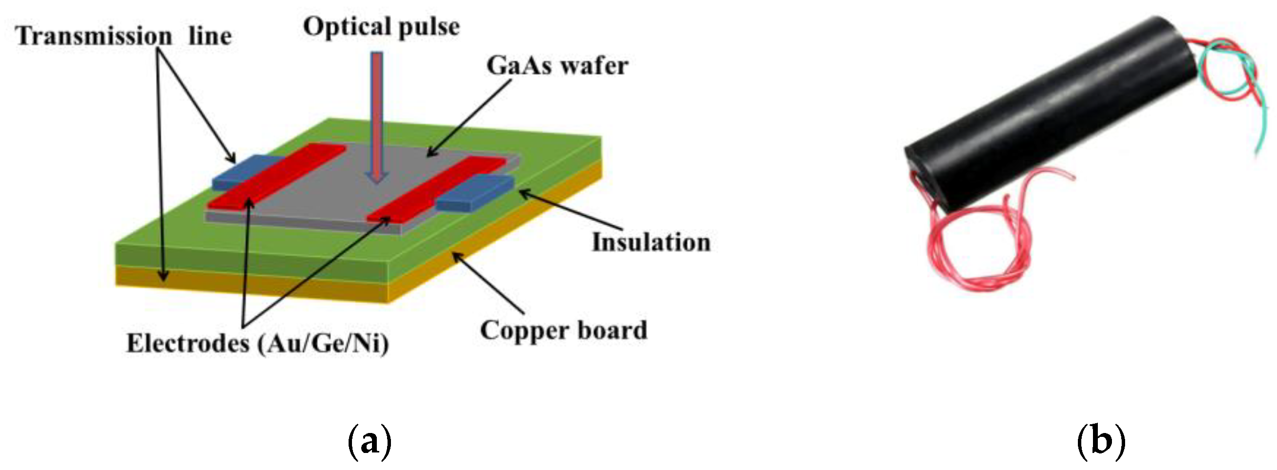
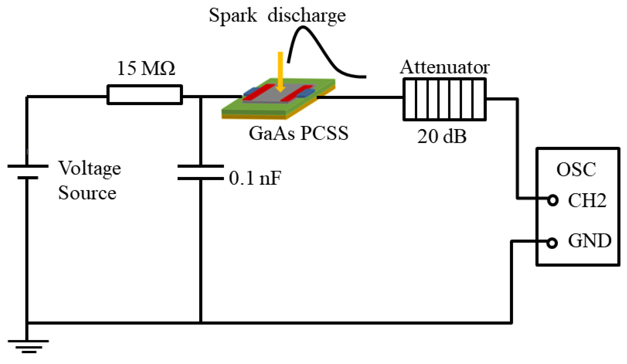
2. Experiment Setup
3. Results and Discussion
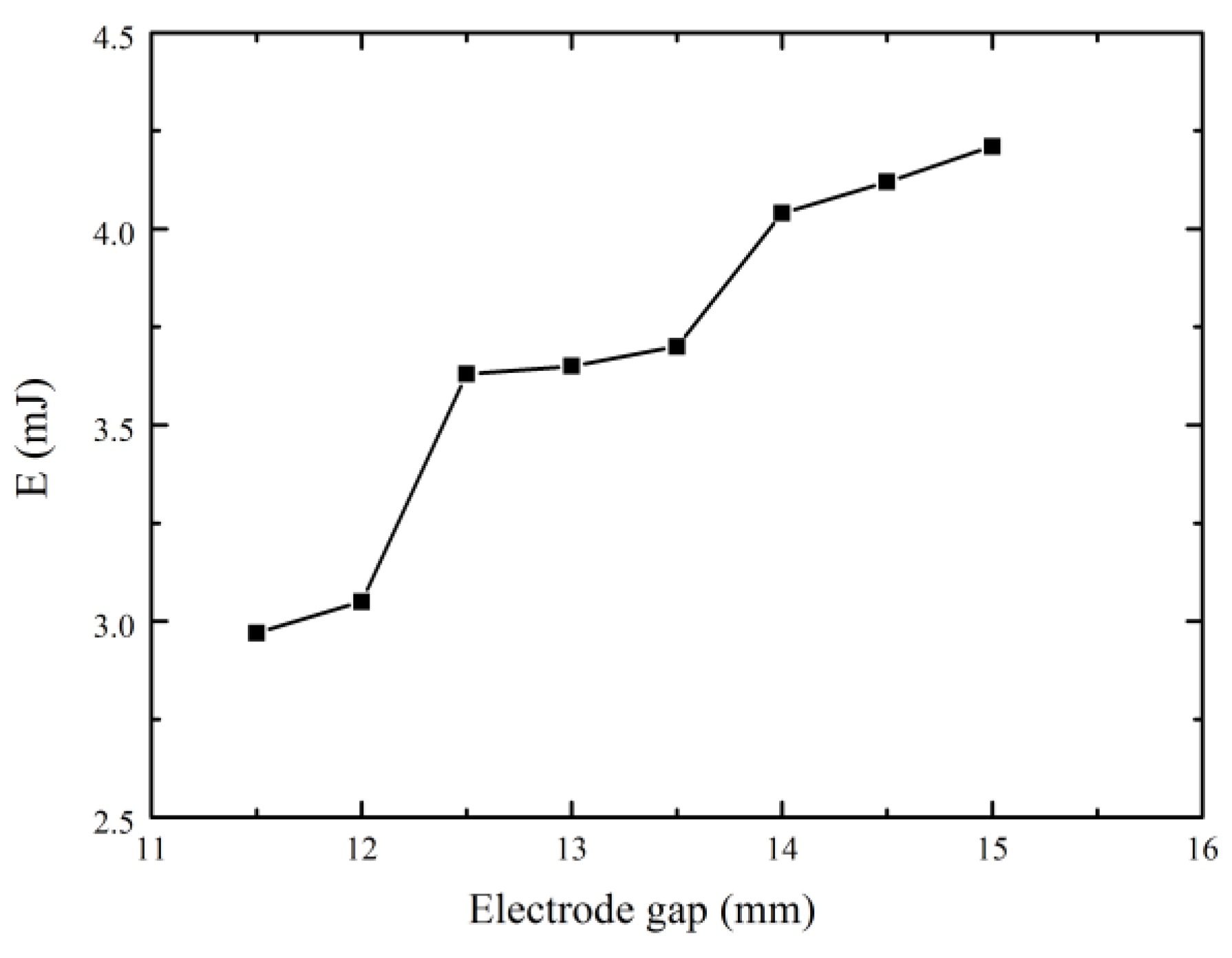
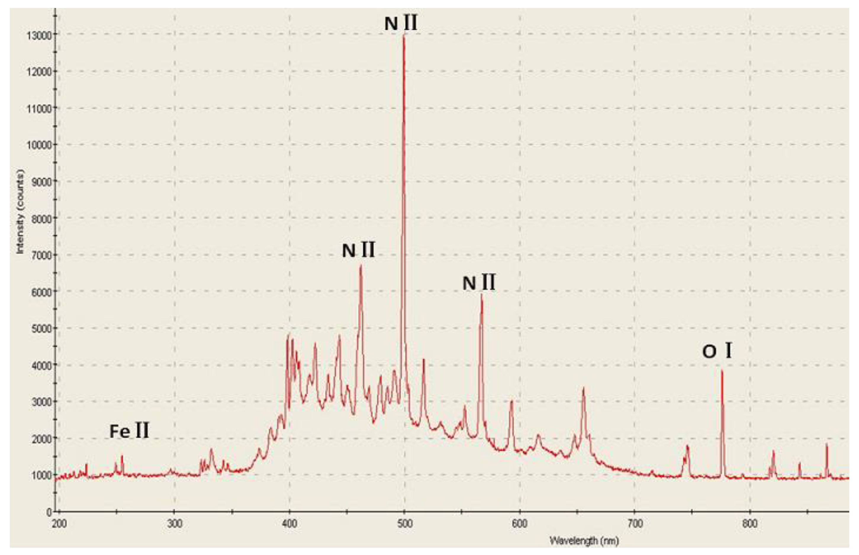
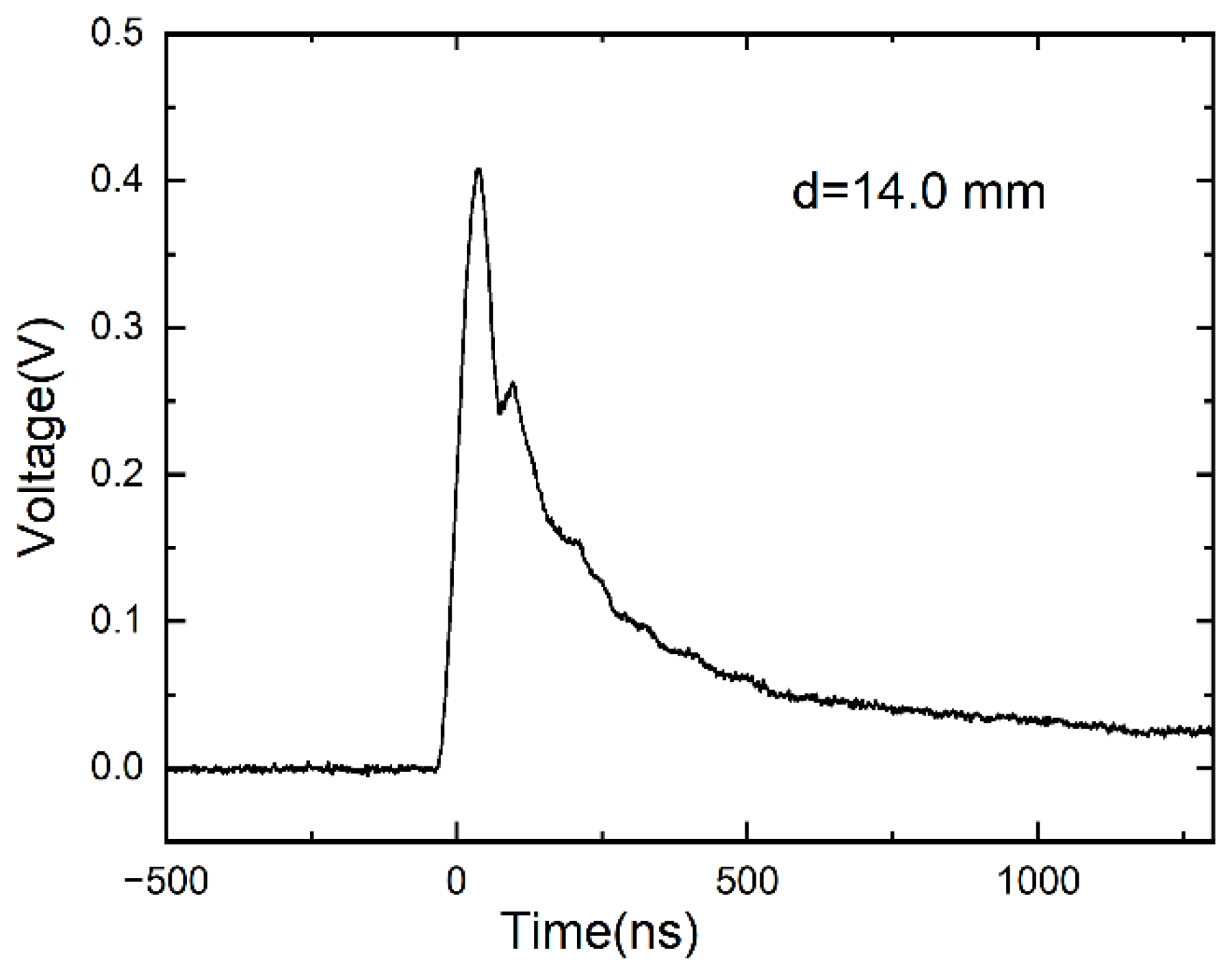
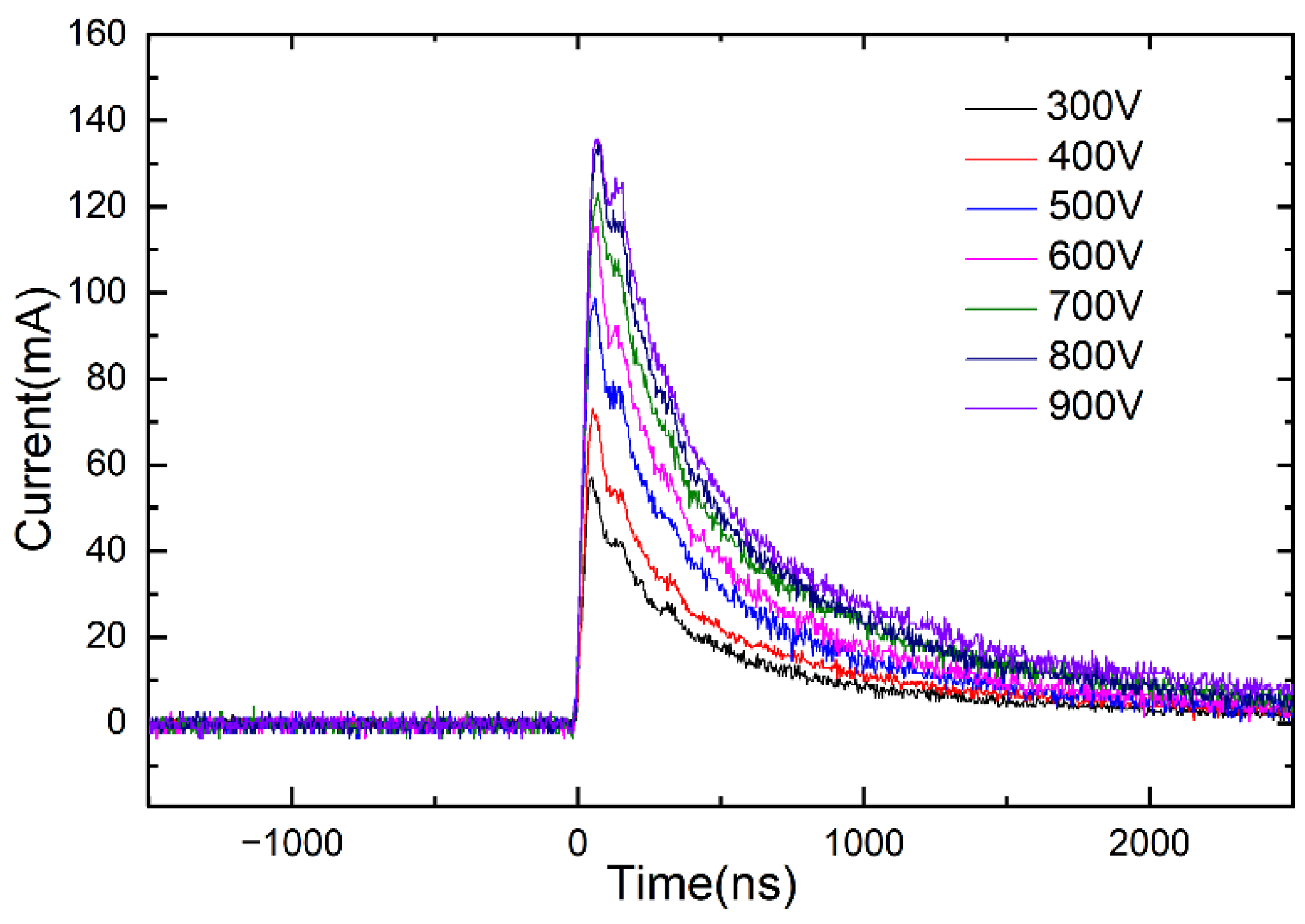
3.1. Spark Discharge Characterization and Evaluation
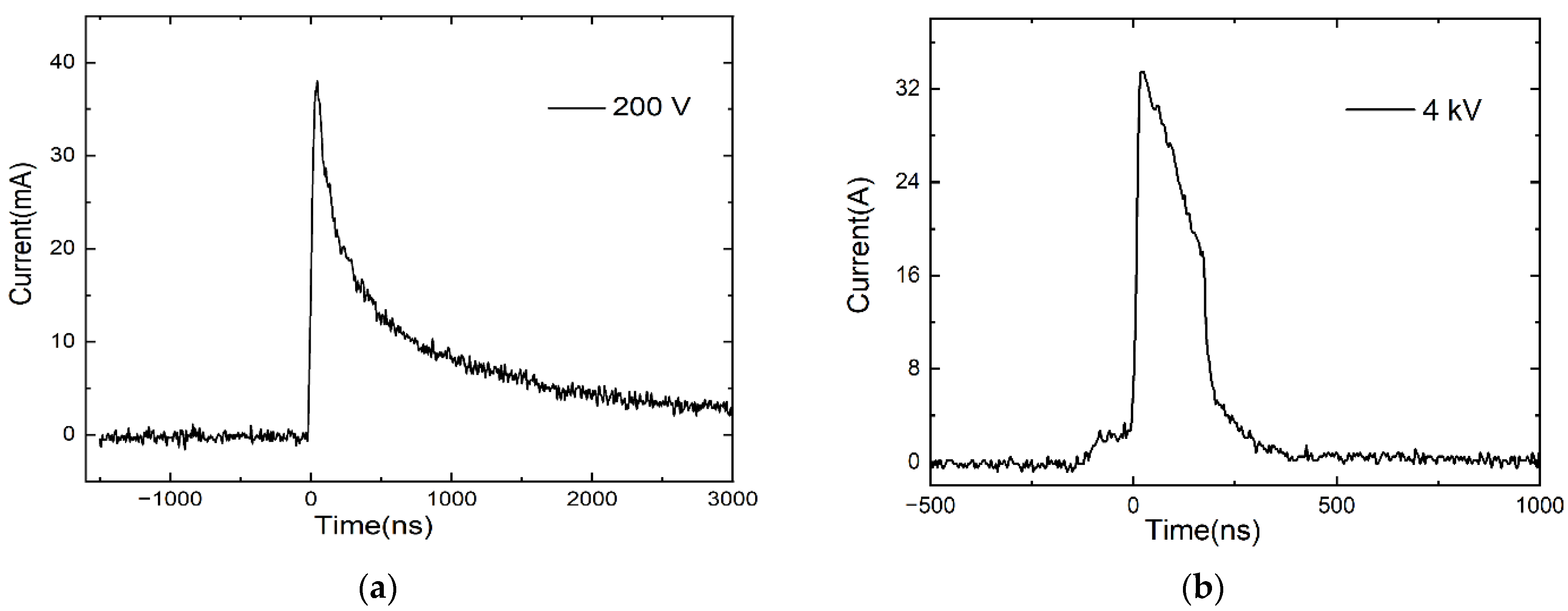
3.2. Triggering the GaAs PCSS
4. Conclusions
Author Contributions
Funding
Data Availability Statement
Conflicts of Interest
References
- Winnerl, S.; Peter, F.; Nitsche, S.; Dreyhaupt, A.; Zimmermann, B.; Wagner, M.; Schneider, H.; Helm, M.; Kohler, K. Generation and detection of THz radiation with scalable antennas based on GaAs substrates with different carrier lifetimes. IEEE J. Sel. Top. Quantum Electron. 2008, 14, 449–457. [Google Scholar] [CrossRef]
- Islam, N.E.; Schamiloglu, E.; Fleddermann, C.B. Characterization of a semi-insulating GaAs photoconductive semiconductor switch for ultrawide band high power microwave applications. Appl. Phys. Lett. 1998, 73, 1988–1990. [Google Scholar] [CrossRef]
- Ajram, S.; Salmer, G. Ultrahigh frequency DC-to-DC converters using GaAs Power switches. IEEE. Trans. Power Electron. 2011, 16, 594–602. [Google Scholar] [CrossRef]
- Nunnally, W.C.; Hammond, R.B. 80-MW photoconductor power switch. Appl. Phys. Lett. 1984, 44, 980–982. [Google Scholar] [CrossRef]
- Loubriel, G.M.; Helgeson, W.D. Triggering GaAs lock-on switches with laser diode arrays. IEEE Trans. Electron. Devices 1991, 38, 692–695. [Google Scholar] [CrossRef]
- Shi, W.; Jiang, H.; Li, M.; Ma, C.; Gui, H.; Wang, L.; Xue, P.; Fu, Z.; Cao, J. Investigation of electric field threshold of GaAs photoconductive semiconductor switch triggered by 1.6 μJ laser diode. Appl. Phys. Lett. 2014, 104, 042108. [Google Scholar] [CrossRef]
- Shi, W.; Hao, N.; Fu, Z.; Li, M.; Ma, C.; Gui, H.; Wang, L.; Jiang, H.; Cao, J. Large current GaAs PCSS triggered by a laser diode. IEEE Photonics Technol. Lett. 2014, 26, 2158–2161. [Google Scholar] [CrossRef]
- Xu, M.; Liu, R.; Shang, X.; Zhang, Q.; Shi, W.; Guo, G. High-Gain Operation of GaAs Photoconductive Semiconductor Switch at 24.3 nJ Excitation. IEEE Electron. Device Lett. 2016, 37, 751–753. [Google Scholar] [CrossRef]
- Mauch, D.; Hettler, C.; Sullivan, W.W.; Neuber, A.A.; Dickens, J. Evaluation of a Pulsed Ultraviolet Light-Emitting Diode for Triggering Photoconductive Semiconductor Switches. IEEE Trans. Plasma Sci. 2015, 43, 2182–2186. [Google Scholar] [CrossRef]
- Dheilly, N.; Paques, G.; Scharnholz, S.; Bevilacqua, P.; Raynaud, C.; Nguyen, D.M.; De Doncker, R.W.; Planson, D. Optical triggering of SiC thyristors using UV LEDs. Electron. Lett. 2011, 47, 459–460. [Google Scholar] [CrossRef]
- Megherbi, M.L.; Bencherif, H.; Dehimi, L.; Mallemace, E.D.; Rao, S.; Pezzimenti, F.; Della Corte, F.G. An Efficient 4H-SiC Photodiode for UV Sensing Applications. Electronics 2021, 10, 2517. [Google Scholar] [CrossRef]
- Ren, W.; Jiang, C. LED-Triggered Photoconductive Semiconductor Switches for Nanosecond Pulse Generation. In Proceedings of the IEEE International Power Modulator and High Voltage Conference, San Francisco, CA, USA, 6–9 July 2016. [Google Scholar]
- Jin, S.; Nie, L.; Zhou, R.; Luo, J.; Lu, X. An Ionization-Driven Air Plasma Jet. Front. Phys. 2022, 10, 528. [Google Scholar] [CrossRef]
- Michelarakis, M.; Clark, D.; Widger, P.; Beroual, A.; Waters, R.T.; Haddad, M.A. Triple Point Surface Discharge Photography in Atmospheric Gases Using Intensified High-Speed Camera System. IEEE Trans. Dielectr. Electr. Insul. 2022, 29, 153–161. [Google Scholar] [CrossRef]
- Palomares, J.M.; Kohut, A.; Galbacs, G.; Engeln, R.; Geretovszky, Z. A time-resolved imaging and electrical study on a high current atmospheric pressure spark discharge. J. Appl. Phys. 2015, 118, 233305-1–233305-11. [Google Scholar] [CrossRef]
- Dubinov, A.E.; Lyubimtseva, V.A. Triggering of Venus Flytrap with Nanosecond Spark Discharges. IEEE Trans. Plasma Sci. 2022, 50, 1710–1714. [Google Scholar] [CrossRef]
- Dubinov, A.E.; Kozhayeva, J.P.; Golovanov, V.V.; Selemir, V.D. Coalescence of Liquid Droplets Under Effect of Pulsed-Periodic Spark Discharges. IEEE Trans. Plasma Sci. 2019, 47, 76–80. [Google Scholar] [CrossRef]
- Brozel, M.; Stillman, G. Properties of Gallium Arsenide, 3rd ed.; The Institution of Electrical Engineers: London, UK, 1996; pp. 135–141. [Google Scholar]
- Shi, W.; Wang, S.; Ma, C.; Xu, M. Generation of an ultra-short electrical pulse with width shorter than the excitation laser. Sci. Rep. 2016, 6, 27577. [Google Scholar] [CrossRef] [Green Version]

Publisher’s Note: MDPI stays neutral with regard to jurisdictional claims in published maps and institutional affiliations. |
© 2022 by the authors. Licensee MDPI, Basel, Switzerland. This article is an open access article distributed under the terms and conditions of the Creative Commons Attribution (CC BY) license (https://creativecommons.org/licenses/by/4.0/).
Share and Cite
Zhang, Q.; Shi, W.; Ma, C.; Yang, L. Evaluation of Pulsed Spark Discharge for Triggering GaAs Photoconductive Semiconductor Switches. Electronics 2022, 11, 2954. https://doi.org/10.3390/electronics11182954
Zhang Q, Shi W, Ma C, Yang L. Evaluation of Pulsed Spark Discharge for Triggering GaAs Photoconductive Semiconductor Switches. Electronics. 2022; 11(18):2954. https://doi.org/10.3390/electronics11182954
Chicago/Turabian StyleZhang, Qin, Wei Shi, Cheng Ma, and Lei Yang. 2022. "Evaluation of Pulsed Spark Discharge for Triggering GaAs Photoconductive Semiconductor Switches" Electronics 11, no. 18: 2954. https://doi.org/10.3390/electronics11182954