Article

Development of Two-Stage Quartz-Crystal Oscillators Using Monolithic Four-Terminal CFOAs

by
Ivailo Milanov Pandiev
Department of Electronics, Faculty of Electronic Engineering and Technologies (FEET), Technical University of Sofia, 1000 Sofia, Bulgaria
Electronics 2022, 11(19), 3027; https://doi.org/10.3390/electronics11193027
Submission received: 2 September 2022 / Revised: 16 September 2022 / Accepted: 20 September 2022 / Published: 23 September 2022
(This article belongs to the Section Circuit and Signal Processing)

Abstract

:
In this article, based on the well-known circuits of two-stage quartz-crystal oscillators, three electronic circuits with a small number of external components are presented. For the proposed circuit configurations, the active elements are composed of monolithic current-feedback operational amplifiers (CFOAs) with access to terminal z, between the first stage (positive second-generation current conveyor (CCII)) and the second stage (output buffer). In this way, the output signal for the developed circuits is obtained after the output buffer of the second CFOA, thereby providing a minimal effect on the resonant circuit of the oscillators. Based on a theoretical analysis of the operational principle for the proposed circuits, the linear characteristic equations and the related self-oscillation conditions are obtained. Moreover, the frequency stability coefficients are determined, which can be obtained with larger values compared to the coefficients of the known discrete transistor circuits. To verify the operability and efficiency of the proposed oscillator circuits, experimental results obtained from sample electronic circuits are presented, which confirm the analyses performed in the frequency range up to about 10 MHz.

1. Introduction

Although more than twenty years old, the current
conveyor appears to be an ‘idea whose time has come’ [1].
A. S. Sedra, G. W. Roberts, and F. Gohh
Quartz-crystal oscillators have a wide practical application, not only in telecommunications systems but also in medical equipment, various measuring instruments, and household appliances. There are almost no electronic modules or systems in which at least one oscillator circuit is not included. For example, the high-performance quartz-crystal oscillators are widely used for electronic watches [2], thermal or electrochemical harvesting devices [3,4], and sensor technology, where we can measure small changes in capacitance and inductance or, on this basis, other quantities with very high accuracy [5,6,7].
The main advantages of quartz-crystal oscillators are that the provided output periodic signal is very stable (with time and temperature) and high selectivity (having very high equivalent Q—factors) [8,9]. A disadvantage of crystal oscillators is that they work at a single frequency, i.e., it is relatively difficult to implement oscillators of those types with frequency tuning over a wide frequency range. The crystal oscillators are most often used in the frequency range from 100 kHz to several tens of megahertz. For frequency control of the crystal oscillators, an external connection of frequency dividers or frequency multipliers is usually required. The analysis of the literature sources showed a wide variety of circuit configurations [10,11,12,13,14,15,16,17,18] of different types of crystal oscillators. Moreover, in the larger number of the presented electronic circuits, transistors (BITs or FETs) are used as active elements compared to the circuit configurations with operational amplifiers (op-amps). This is due to the possibility of obtaining crystal oscillators operating up to a higher frequency and with the higher stability of the parameters of the output signal, such as amplitude and frequency. Moreover, the use of op-amps in many cases requires adding auxiliary passive and active elements or even functional blocks providing input/output resistance according to the requirements of the resonant circuit (also known as a tank circuit [9] or simply LC tank [8]) or amplitude and frequency control [11,13,14,15].
One possible method to simplify the circuit structure and improve the electrical parameters of crystal oscillators with op-amps as active elements is by using monolithic positive second-generation current conveyors (CCII+s) [1,19] or monolithic four-terminal current-feedback operational amplifiers (CFOAs) [20,21,22]. These types of op-amps are characterized by one non-inverting high-impedance input terminal—y, one inverting low-impedance input terminal—x, and one high-impedance output terminal—z in the CCII+. The four-terminal CFOAs also include a buffered output stage that converts the output current produced in the high-impedance output terminal of the CCII+ into a voltage, at which the output terminal (o) has relatively very small output resistance. For the four-terminal CFOAs, terminal z is defined as an external terminal accessible for electrical connections [22,23]. The analysis of the literature sources showed a relatively small number of circuit configurations of quartz-crystal oscillators [24,25,26,27,28] in which monolithic CCII+s or four-terminal CFOAs are used as active elements. On the one hand, this is due to the specific internal structure and working principle of this type of monolithic amplifier circuit, and on the other hand, there is a relatively small number of commercially available CCII+s or four-terminal CFOAs, which is probably soon to be overcome as a practical drawback. Examples of commercially available integrated circuits (ICs) of this type are OPA860 [29] and OPA861 [30] by Texas Instruments, as well as AD844 [31] by Analog Devices. Moreover, in some practical cases, the IC LT1228 [32] from Analog Devices (previously from Linear Technology) may be used.
Based on the two-stage self-limiting series mode type quartz-crystal oscillators presented in [10] and some applied circuit configurations given in [21,22,23,27], in this work, the author has tried to develop electronic circuits of two-stage quartz-crystal oscillators containing a minimum number of external passive components and providing the possibility for high stability (high value of the equivalent quality factor). Furthermore, some of the circuit variants used crystal units operated at the series resonant frequency, and the other circuits used crystal units operated at a frequency slightly above series resonance, where the equivalent impedance is with a positive sign (or has inductive character).
The structure of this paper is as follows. Section 2 presents the structure of the basic equivalent circuits and the electrical parameters for the monolithic CFOAs with externally available z-terminal. Moreover, Section 2 shows the equivalent circuit of a current conveyor, represented as an equivalent bipolar transistor of NPN or PNP type (or MOS transistor of N- or P-type), depending on the polarity of the input differential voltage. In Section 3, the proposed electronic circuits are presented and a theoretical analysis in the stationary mode of operation is presented, in which, based on the obtained characteristic equations, formulas for the self-oscillation conditions and sensitivity coefficients are derived. To verify the performed theoretical analyses in Section 4, the results of simulation and experimental testing are presented. For all oscillograms and characteristics, comments and conclusions are presented. Finally, in Section 4 of this paper, the concluding remarks and the highlights for the developed electronic circuits are given.

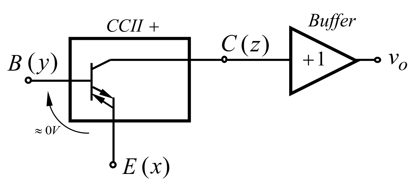
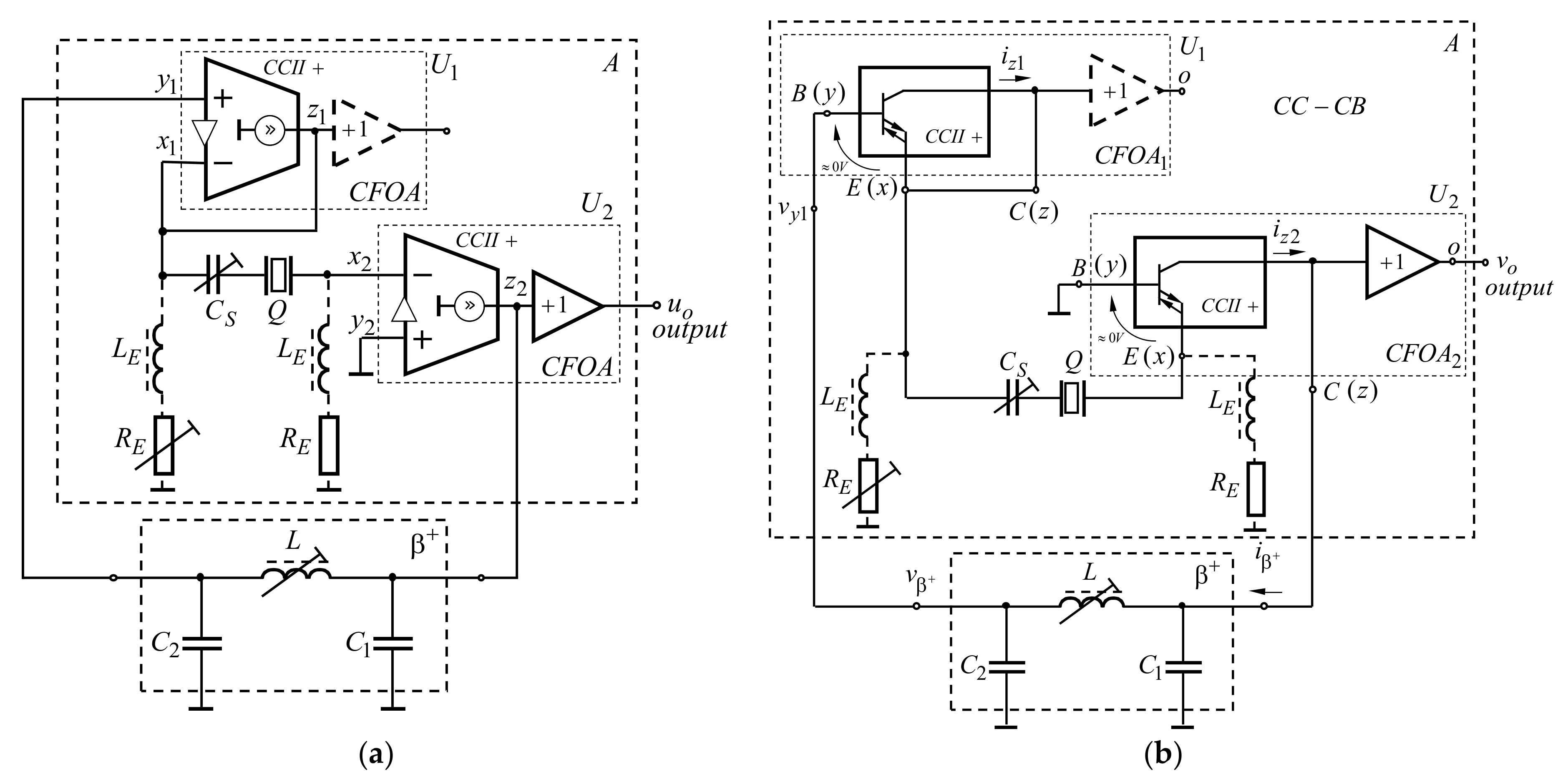
2. Structure and Basic Parameters of the Monolithic CFOAs with Externally Available z-Terminal

The symbolic representation of a four-terminal CFOA is shown in Figure 1a, and the equivalent circuit diagram is shown in Figure 1b. As can be seen, this type of monolithic amplifier can be presented as a cascade structure of a CCII+ and an output voltage follower (voltage buffer). The equivalent circuit includes one ideal input buffer with unity voltage gain; current-controlled current source (CCCS) with i z i x ; r y and C y —input resistance and capacitance of the non-inverting input terminals; r x —series resistance of the inverting input terminal; r z and C z —output resistance and capacitance of the CCII+ and ideal output buffer with unity voltage gain and zero output impedance.
Then, the output voltage of the CFOA is obtained
v o = i x × Z z = v y x r x × Z z = r z r x × 1 1 + s r z C z v y x ,
where Z z = r z | | 1 s C z is the output impedance of the CCII+ in the structure of the four-terminal CFOA.
Substituting s = jω,
v o ( j ω ) = r z r x × 1 1 + j ω ω p v y x ( j ω ) ,
where ω p = 1 r z C z is the upper 3-dB frequency of the CFOA.
As can be seen from the above expression, the dominant pole (or upper 3-dB frequency) in the frequency response of the CFOA is determined by the parameters of the output network of the CCII+. The second pole is determined by the input network of its non-inverting input terminal.
Based on Equation (2), the open-loop voltage gain at low frequencies can be obtained as A d 0 = v o v y x = r z r x . If an external resistor R C to ground is connected to terminal z (in parallel with the output resistance r z ), the voltage gain is found A d 0 = r z | | R C r x G m ( r z | | R C ) , where G m 1 / r x is the equivalent overall transconductance of the CCII+, determined by the value of the IC bias current. Moreover, if terminal z is connected to the ground, and a resistor RE is connected to terminal x to the ground, since the operating point is set internally, and assuming V y x = 0 , then the transmission coefficient is A v = v x v y = R E r x + R E < 1 . A transmission coefficient approximately equal to unity can also be obtained provided that terminal z is connected to terminal x. This doubles the output current since the current iz has the same polarity as the current ix, then A v = v x v y = R E R E + r x / 2 1 .
If this operation is compared with the physical operation of a classical bipolar junction transistor (BJT), it may be concluded that the first stage of the CFOA can operate both as an NPN and as a PNP transistor (Figure 2), depending on the polarity of the input differential voltage v y x . The comparative analysis shows that, if the v y x > 0 , the output stage of the CCII+ is sourcing current iz to the equivalent load; however, its direction is opposite to the direction of the collector current in the classical NPN transistor. If v y x < 0 , the output stage of the CCII+ is sinking current iz from the equivalent load, which is equivalent of the operation to the PNP transistor, but with opposite direction of the collector current.
This analogy in the principle of operation of the current conveyors can be used in the development of quartz-crystal oscillators based on well-known circuit configurations [8,9,10,11] with discrete transistors as active elements.

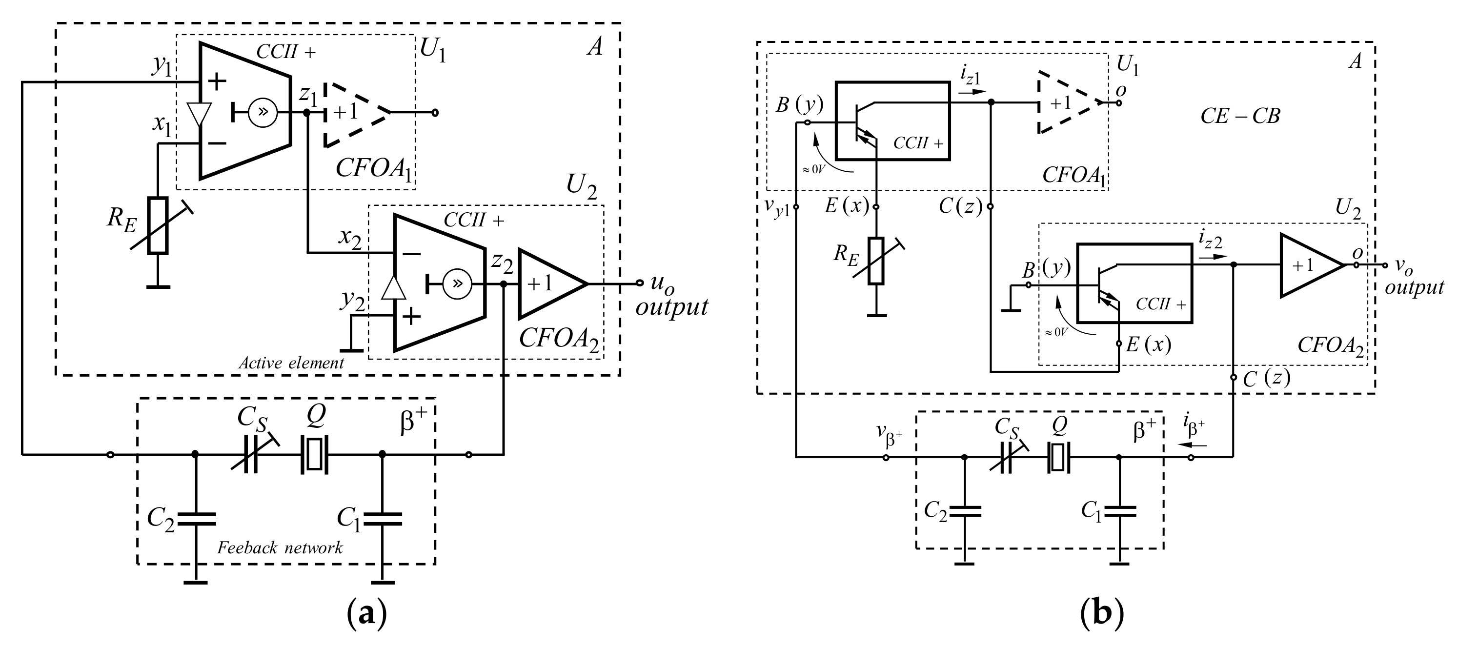
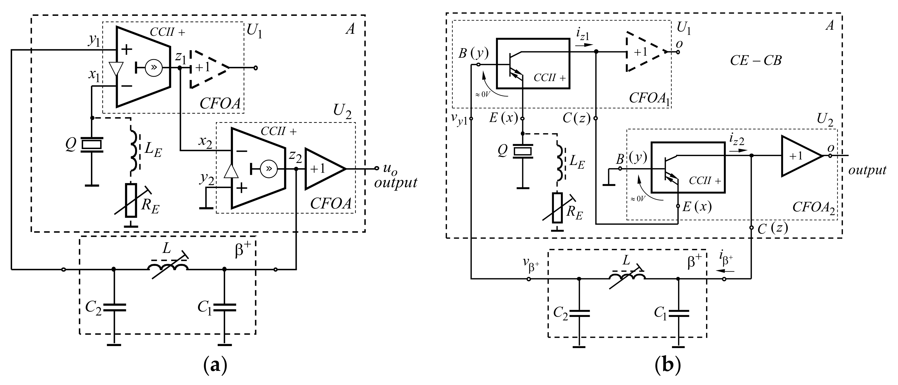
3. Theoretical Analysis of the Developed Two-Stage Oscillators

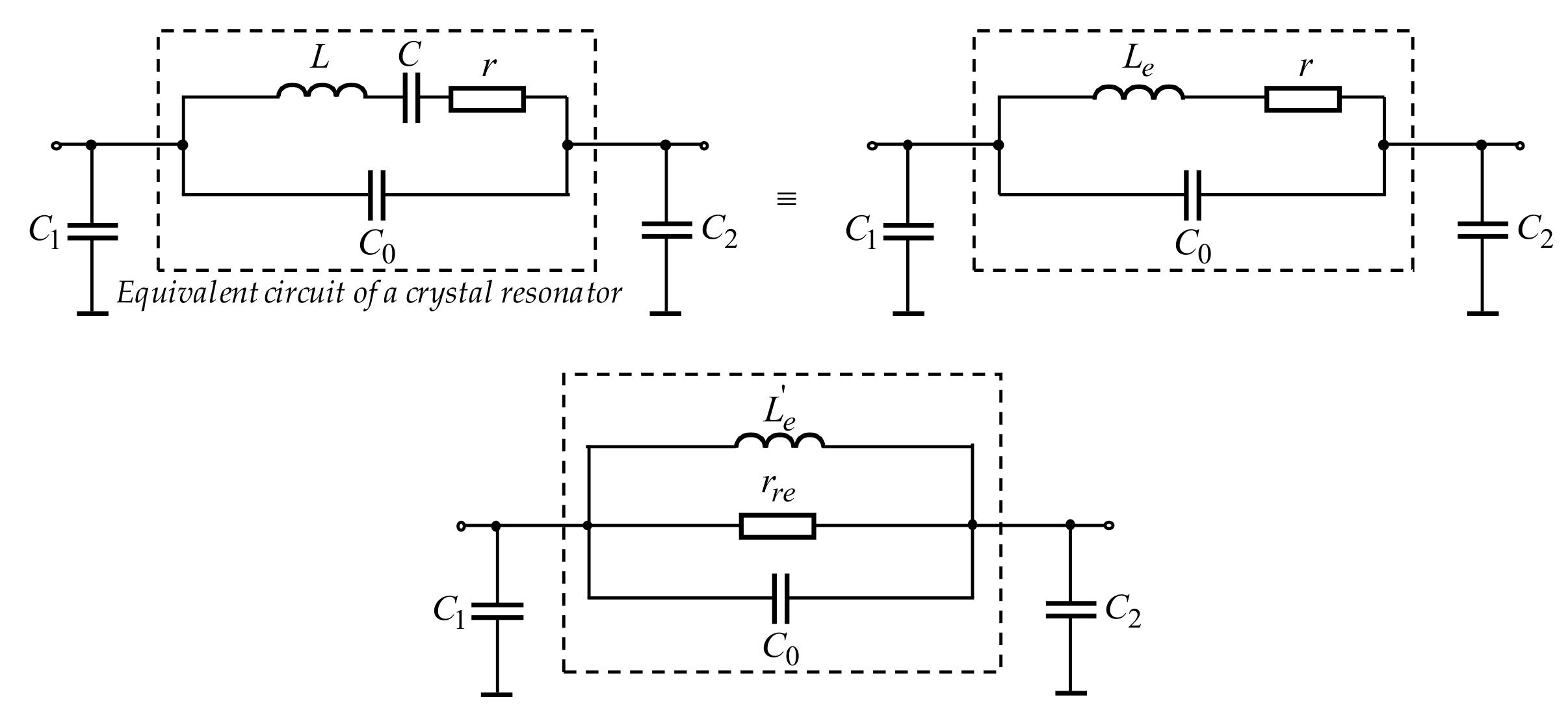
3.1. Two-Stage Oscillator with Quartz-Crystal Resonator, Which Is Behaving as an Inductor

Based on the structure and the description of the principle of operation of the monolithic four-terminal CFOAs, as well as the basic structures of the quartz-crystal oscillators with discrete transistors, in Figure 3 is shown the first proposed configuration of a two-stage oscillator (QO1) using a quartz crystal resonator, which is behaving as an inductor, or the branch reactance of the used crystal unit is positive (or with inductive characteristic). This electronic circuit is similar to the two-stage Pierce-type oscillator with discrete transistors as active elements. For the LC oscillator in Figure 3a, the active element is composed of two four-terminal CFOAs, connected in a cascaded structure. As can be seen, only the first stage—CCII+ is used for the U1, and the terminal z1 is connected to the terminal x2 of the U2. The grounded trimmer-potentiometer RE is connected to terminal x1, which is used to adjust the amplitude of the output sinusoidal signal. By changing the value of the RE, the voltage gain is changed and when the supply voltage is turned on, the self-oscillation process is started. Terminal z2 of the U2 is connected to one end of the positive feedback network. The positive feedback network is closed by connecting its output to the high-impedance terminal y1 of the U1. The output sinusoidal signal of the oscillator is obtained from the output port of the second stage-voltage follower (buffer) of the U2. Since the second stage of the U2 has a high input resistance and a low output resistance, the influence of the load parameters on the positive feedback parameters is minimized.
By analogy with the oscillators employing discrete transistors in Figure 3b, each of the CCII+s is represented as a bipolar transistor, with a voltage between the equivalent base and emitter approximately equal to zero. Furthermore, these transistors can operate as an NPN or PNP transistor depending on the polarity of the voltage between the equivalent base and emitter. Unlike the classic transistors, at a positive input voltage, the output stage of the CCII+ is sourcing current iz to the equivalent load (CCII+ pushes its current iz into the next stage), i.e., the common-emitter equivalent circuit will be a non-inverting configuration and the common-base equivalent circuit will be inverting circuit configuration. Therefore, according to the way of connecting the two equivalent transistors, a common emitter (CE)–common base (CB) cascode configuration (or CE–CB amplifier) is obtained. The cascode amplifiers are analog circuits in which the active elements (BJTs or FETs) are connected in series for a direct current (dc) and cascade for an alternating current (ac) [33]. The cascade connection means that if we take a two-transistor cascode as an example, the output voltage of the first transistor is the input voltage of the second. The cascoding refers to the use of a transistor connected in the common-emitter (or the common-source) configuration to provide voltage buffering for the input of a common-base (or a common-gate) amplifying transistor. Using a cascode configuration achieves a wider bandwidth and higher input impedance. Moreover, for the medium frequencies, the phase shift of the output voltage according to the input voltage, approximately equal to 180°, is obtained.
The positive feedback of the oscillator in Figure 3 includes one quartz-crystal resonator Q, trimmer capacitor CS, and two grounded capacitors (C1 and C2). In this case, the crystal unit operates at a frequency slightly higher than the frequency of the series resonance. For this frequency, the reactance of the crystal unit is positive and has an inductive character, i.e., the quartz resonator behaves as an inductor. To maintain the oscillation above the series resonance frequency, a trimmer capacitor CS is connected in series to the crystal Q. This will compensate the initial inductance of the crystal with an additional inductance or capacitance. Moreover, the inclusion of a trimmer capacitor does not change the parallel resonance frequency f s = f S 1 + C C o + C S f s 1 + C 2 C o + C S (at C < < C o + C S and using the equality 1 ± x 1 ± 1 2 x (for x < < 1 )), but if the value of the CS is reduced, the series resonance frequency will close to the parallel resonance frequency of the crystal.
In order to derive analytical expressions for designing the proposed oscillator, Figure 4 shows the equivalent circuit of the crystal resonator and the capacitors C1 and C2 connected to it [12,34]. In Figure 4, the components L, C, and r define the parameters of the series mechanical resonance, and the capacitance Co models the capacitance of the electrodes with the quartz plate as a dielectric (or electrode-plus-holder capacity). The value of the equivalent inductance can be determined based on the following transformations of the motional impedance:
Z L C = r + j ω L 1 1 ω 2 L C = r + j ω L 1 ω s 2 ω 2 L e
where L e = L 1 ω s 2 ω 2 and ω s = 1 L C is the series-resonant frequency (or the mechanical resonant frequency) of the crystal unit.
For the standard (angular) frequency ω Q specified by a certain manufacturer, at the specified load capacitance, the value of the equivalent inductance is obtained
L e = L 1 ω s 2 ω Q 2
As can be seen from the above expression, since ω Q > ω s , then L e < L .
To obtain a parallel equivalent circuit of the crystal unit to be used in forming the characteristic equation of the proposed oscillator, the equivalent admittance of the circuit is determined
Y e = 1 r + j ω L e = r r 2 + ( ω L e ) 2 j ω L e r 2 + ( ω L e ) 2 = 1 r r e j ω 1 ω 2 L e .
After equating the left and right sides of the above expression, the parameters of the parallel equivalent circuit are obtained
r r e = r 2 + ( ω L e ) 2 r ω L e > > r ( ω L e ) 2 r   and
L e = L e r 2 + ( ω L e ) 2 ( ω L e ) 2 ω L e > > r L e .
To determine a formula for the frequency of oscillations and the condition for the oscillations, the feedback loop is broken and the loop gain L ( s ) A ( s ) × β + ( s ) is determined. The feedback loop is interrupted at the node that connects the positive feedback with the input terminal y1 of the first active element U1. On the basis of the resulting circuit, to the input of the amplifier U1 is applied a voltage vi, then A ( s ) i z 2 ( s ) / v i ( s ) and β + ( s ) v β + ( s ) / i z 2 ( s ) are determined separately, and hence the loop gain L ( s ) is found. The characteristic equation for the oscillator circuit with positive feedback is
1 L ( s ) = 0 .
Using the small-signal equivalent circuit of a CFOA (Figure 1b) and by the nodal method, analysis for the linear characteristic equation of the QO1 is obtained
1 s C 0 + 1 s L e s C 1 + s C 0 + 1 s L e s C 2 + s C 0 + 1 s L e s C 0 + 1 s L e + 1 r o e × 1 r x + R E + R E r x r z = 0 ,
where r o e ( ω L e ) 2 r is the equivalent resonance resistance, C 1 = C 1 + C z + C M ( C M is the board parasitic capacitances with typical value within the range from 3 up to 5 pF according to the type and quality of the used prototype board), and C 2 = C 2 + C y + C M .
Substituting s = jω after some transformations of Equation (9) obtains
1 r x + R E + R E r x r z 2 r o e ω 2 C 0 L e r x + R E + R E r x r z + 2 ω 2 C 0 L e r o e + j ω ( C 1 + C 2 ) ω 3 [ C 1 C 2 + ( C 1 + C 2 ) C 0 ] L e 0 .
For oscillations to occur at the output port of the circuit in Figure 3, both the real and the imaginary part of the Equation (10) have to be equal to zero. Equating the imaginary part to zero gives the expression for the frequency of oscillations (FO)
ω 0 = 1 L e C 1 C 2 C 1 + C 2 + C 0
and equating the real part to zero gives the following expression for the condition of oscillation (CO)
r o e r x + R E + R E r x r z + 2 C 0 C 12 + C 0 = 2 + r o e r x + R E + R E r x r z C 0 C 12 + C 0 .
By selecting C 1 = C 2 = 2 C or C 12 = C , the condition of oscillation is simplified and yields the form
r o e r x + R E + R E r x r z = 2 .
As can be seen from Equation (13), provided that the capacitances C 1 and C 2 have equal values, the condition of oscillation does not depend on the frequency of oscillations. This is especially important when the frequency of oscillations and the amplitude of the output signal are tuning at the initial starting of the electronic circuit by applying supply voltages.
Moreover, to start oscillations, the amplification of the active element must be greater than 2; in an analytical form the condition can be presented in the following form
G m r o e 1 + G m R E + R E r z > 2 .
Since the amplitude of the output signal increases in the process of self-oscillations due to the internal nonlinearity of the active element, the equivalent conductance Gm decreases and, accordingly, the loop gain decreases to unity, thus oscillations with constant amplitude and frequency result.
The passive sensitivities of the QO1 are relatively low values and expressed as
S C 1 ω 0 = 0.5 C 2 C 1 + C 2 ,   S C 2 ω 0 = 0.5 C 1 C 1 + C 2 , and S L e ω 0 = 0.5 .
Another important advantage of the two-stage oscillator in Figure 3 is the ability to obtain a coefficient of frequency stability, higher than unity in a relatively wide operating range:
S F = d Φ ( ω ^ ) d ω ^ ω ^ = 1 2 Q x 2 ρ r o e ,
where ρ = L / C is the characteristic resistance of the crystal unit, ω ^ = ω / ω o is the normalized angular frequency, Qx is the equivalent quality factor, and Φ ( ω ^ ) = arg [ L ( ω ^ ) ] represents the phase function of the loop gain with breaking of the feedback loop at the input of the U1.
As can be seen from Equation (15), an increase in the equivalent quality factor Qx leads to a larger value of the frequency stability coefficient. In addition, a larger value of the quality factor will provide better selectivity and smaller amplitude of higher harmonics, and therefore a smaller value of nonlinear distortions. However, when the initial value of the loop gain L ( s ) is larger (relative to the unity value), i.e., when the requirement is to obtain a larger amplitude of the output sinusoidal signal, the voltage drop across the quartz unit increases, and this leads to a decrease in the equivalent quality factor and a certain increase in nonlinear distortions.

3.2. Two-Stage Series-Mode Crystal Oscillators

Based on the structures of the bridged-T type circuits [10,35] with vacuum tubes or discrete transistors, in Figure 5 is shown the second proposed configuration of a two-stage oscillator (QO2) using a crystal unit, operating at the series-resonant frequency. In this case, the reactive impedance is purely resistive, with a value approximately equal to several tens of ohms. As can be seen, the resonant circuit of the developed oscillator is similar to a Colpitts oscillator type feedback network arrangement. For the circuit in Figure 5a, the active element is implemented of two four-terminal CFOAs, connected in a cascaded structure—terminal z1 of the U1 is connected to terminal x2 of the U2. The crystal unit is connected to terminal x1 of the U1. By analogy, with the oscillators using discrete bipolar transistors in Figure 5b, each of the CCII+s is represented as a bipolar transistor. As a result of the way of connecting the two equivalent transistors, a common collector (CC)–common base (CB) cascode configuration (or CC–CE amplifier) is obtained. Additionally, an inductor LE and a trimmer potentiometer RE are connected in series to terminal x1. By changing the resistance RE, the amplitude of the output signal is adjusted to a certain value. A series-connected inductor LE of the potentiometer RE provides a reduction of the amplification when approaching the frequency of oscillations ω0, as well as a limitation of the value of the parallel resonance frequency, determined by the capacitance Co. Similar to the circuit of Figure 3, the positive feedback network is connected between the terminal z2 of the U2 and the high-impedance terminal y1 of the U1. The output signal of the developed oscillator is produced at the output port of the voltage follower (buffer) of the U2.
Using the equivalent circuit of a CFOA, shown in Figure 1b, and by theoretical analysis for the linear characteristic equation of the QO2, finds
1 1 s 3 C 1 C 2 L + s 2 C 2 L r o e + s ( C 1 + C 2 ) + 1 r o e × 1 r x + r Q + r Q r x r z = 0 ,
where r o e ( ω L ) 2 r L is the equivalent resonance resistance, r Q r | | ( r L E + R E ) is the equivalent resistance at x terminal of the U1, r L E is the ohmic resistance of the inductor LE, r L is the ohmic resistance of the inductor within the resonant circuit, C 1 = C 1 + C z + C M , and C 2 = C 2 + C y + C M .
Substituting s = jω,
1 r o e + 1 r x + r Q + r Q r x r z ω 2 C 2 L r x + r Q + r Q r x r z + j [ ω ( C 1 + C 2 ) ω 3 C 1 C 2 L ] = 0 .
The electronic circuit in Figure 5 is characterized by the following CO and FO, taking into account the effect of parasitic capacitances:
ω 0 = 1 L C 1 C 2 C 1 + C 2
and
r o e r x + r Q + r Q r x r z = C 2 C 1 .
The coefficient of frequency stability for the QO2 is given by
S F = d Φ ( ω ^ ) d ω ^ ω ^ = 1 2 ( Q L C + Q x ) ,
where Q L C = r o e / ρ is the equivalent quality factor of the LC tank and ω ^ = ω / ω o is the normalized angular frequency.
The third electronic circuit (QO3) of a two-stage oscillator was developed based on the well-known Butler circuit8. The circuit diagram of the resulting oscillator with monolithic CCIIs is shown in Figure 6a, and the circuit configuration in which the active elements are represented as bipolar transistors is given in Figure 6b. Unlike the Butler oscillator, in which the active element is a cascode (common emitter–common emitter) configuration operating with positive feedback formed by a quartz unit connected between the two emitters of the first and second stages, the developed oscillator circuit uses a cascode configuration with common collector–common base, as shown in [10], because the common-base equivalent circuit implemented with a CCII inverts the phase of the input signal. For the proposed oscillator, the quartz unit is connected in the forward circuit, between the emitters of the two equivalent transistors. The positive feedback is obtained as the signal from the collector (or terminal z2) of the second equivalent transistor U2 through a selective resonant circuit with the signal that is with a 180° shift for its resonant frequency to the base (or terminal y1) of the first equivalent transistor U1. In this way, the number of external passive components is reduced and conditions are formed for increasing the equivalent quality factor. For the proposed scheme, the oscillation frequency is determined by Equation (18). The oscillation condition is obtained from an active element analysis and is given by
r o e 2 r x + r Q | | z E + R E + r Q r x r z = C 2 C 1
where z E = r L E 2 + ( ω 0 L E ) 2 is the equivalent impedance of the used additional inductor LE and variable resistance RE at oscillation frequency ω0.
The coefficient of frequency stability can be obtained by Equation (20).

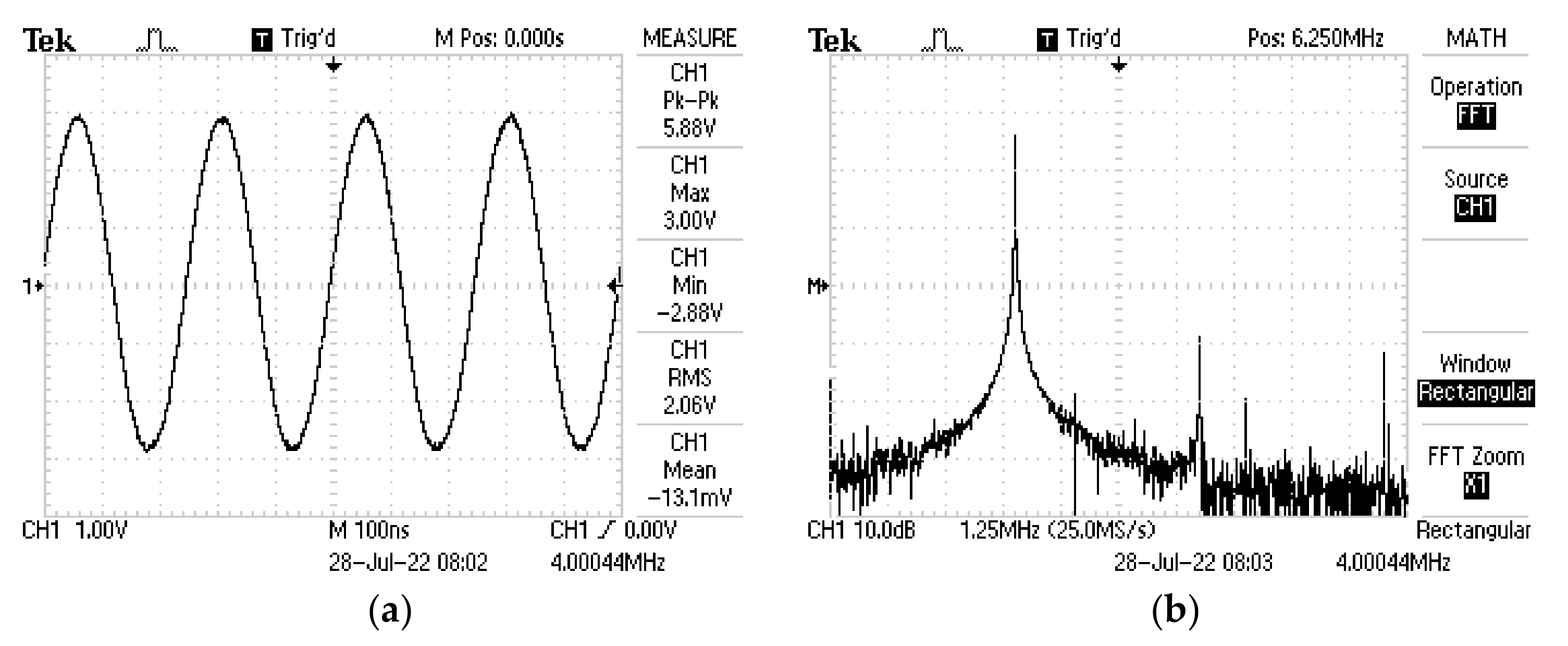
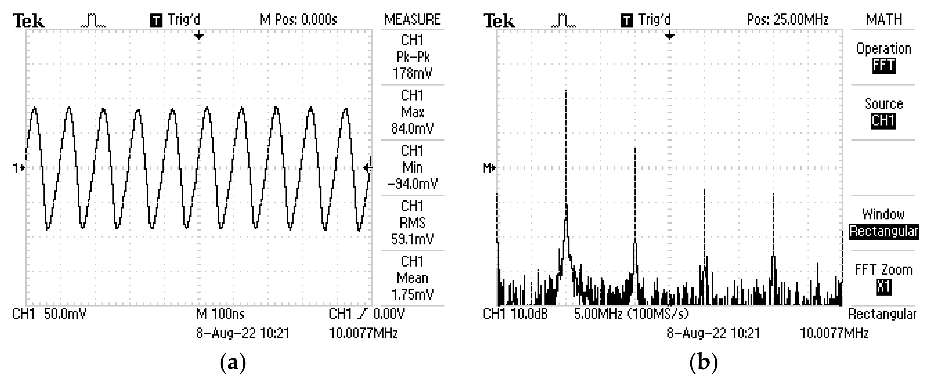
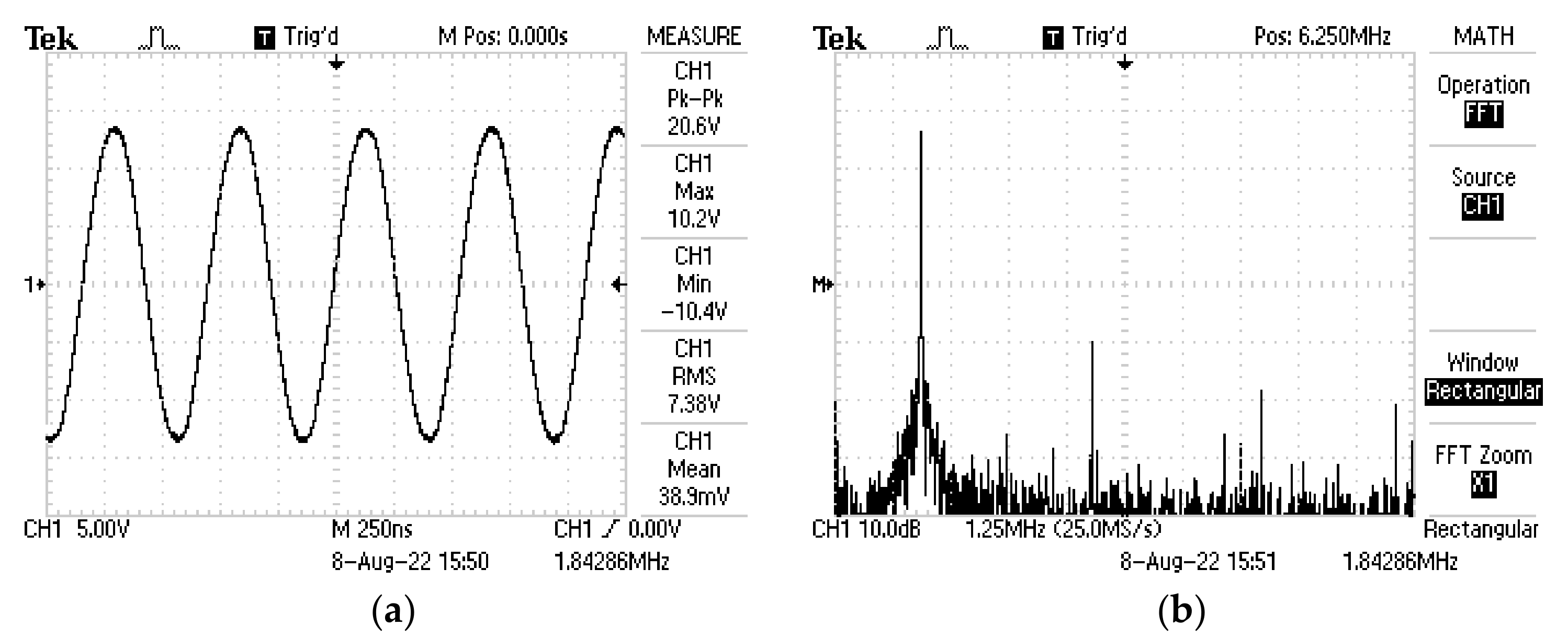
4. Results and Discussion

To verify the reliability of the presented theoretical analyses and derived analytical expressions above, in this section, the results of an experimental study of sample electronic circuits are given. For the experimental study, the electronic circuits were implemented on prototype boards with through-hole active and passive components. All the active and passive components were located on one side of the board, and the other side was used as ground. During the assembly of the electronic circuits, the minimum length and curvature of the connecting wires, as well as a minimal amount of interlacing between the electrical connections, were observed. Moreover, the connection wires were located close to the surface of the board to minimize the possibility of stray inductive coupling.
The experimental testing of the proposed crystal oscillators was performed using the monolithic four-terminal CFOA AD844 [31] (from Analog Devices). To provide the power supply voltages for the active components, a DC linear power supply HY3005D-3 was used, providing two stabilized DC voltages with values ±15 V. The output DC offset voltage of the CFOAs at room temperature (approximately equal to 25 °C) was adjusted approximately to several millivolts, by connecting trimmer potentiometers with a nominal value of 20 kΩ to the two offset-nulling terminals of the CFOAs (pins 1 and 8 of the used IC). The wipers of the potentiometers were connected to the CFOAs positive supply voltage of 15 V. The CFOA AD844 was chosen as an active component because it allows obtaining a relatively wide dynamic range of the input and output voltages, as well as providing good stability of the electrical parameters in a relatively wide frequency range, up to about 60 MHz. As a result, the AD844 has been established as the basic active component in a wide variety of analog processing circuits, employing current conveyors or four-terminal CFOAs.
Crystal resonators with frequencies of 1.8432 MHz, 4.0000 MHz, and 10.0000 MHz [36] were used to build the electronic circuit (QO1) in Figure 3, as well as trimmer capacitors [37] Cs with a capacity of 10 to 30 pF, depending on the frequency of oscillations. According to the recommendations defined in Equations (11)–(13), capacitors C1 and C2 with equal capacities were selected, as the equivalent capacity has a value of 16.5 pF, which is less than the maximum load capacity of the selected crystals, which has to be below 30 pF. To adjust the amplitude of the output sinusoidal signals, multiturn trimmer potentiometers [38] RE with values from 10 to 50 kΩ were used. The output signals with maximum value of the amplitude of the QO1 at frequencies fQ1 = 1.8432 MHz, fQ2 = 4.0000 MHz, and fQ3 = 10.0000 MHz are shown in Figure 7a, Figure 8a and Figure 9a, respectively. The output spectrum of the signals at the same frequencies is given in Figure 7b, Figure 8b and Figure 9b, respectively. The signals are measured at an ambient temperature near 25 °C. As can be seen, as the frequency increases, the amplitude of the output signal decreases, and nonlinear distortions also increase (up to 10%). Further reduction of nonlinear distortions can be achieved by reducing the amplitude of the output signal, adjusting RE, and also by reducing the effect of the parasitic capacitances.
For a change in the ambient temperature over a small range (of the order of a few degrees nearly symmetric with the room temperature) a small change in the frequency of oscillations occurs, which can be neglected. For wide temperature ranges, such as 25 °C to 65 °C, a total frequency shift of ≈0.06% (or the temperature coefficient is approximately equal to 15 ppm/°C) was the result. To control the frequency of the output signals, an Instek GFC-8010H digital frequency counter was used.
Changing the supply voltage by ±5% results in very little change in frequency. The total frequency change is ≈0.01%. This is mainly due to the use of monolithic CFOAs as active elements, in which the operating point is established through internal circuits with a system of current mirrors.
When the supply voltage is turned on, the middle point (wiper) of the trimmer potentiometer RE is placed in a position where the minimum value of the resistance is obtained. In this case, the voltage gain has a maximum value. According to Equation (14), the amplification of the loop gain is greater than unity. As a result, a process of self-oscillations starts, and a signal with a shape close to the sine wave is obtained at the output port. The frequency of the produced output signal has a value close to, but smaller than, the frequency ωQ. By moving the wiper in the direction of increasing the resistance RE, the amplitude of the output signal decreases, while the frequency increases, closing to the frequency ωQ. For a specific frequency ω0 (fundamental (or oscillation) frequency), the loop gain L ( j ω 0 ) A ( j ω 0 ) × β + ( j ω 0 ) is equal to unity and sinusoidal oscillations are obtained at the output of the circuit. This state of the circuit is known as fulfilling the Barkhausen criterion. For it, the output signal has a constant amplitude and frequency. In this case, the frequency ω0 is equal to the frequency ωQ. To fine-tune the frequency of the output signal, in some cases, the trimmer capacitor CS, connected in series to the crystal unit, can be used. If the two frequencies are exactly equal, the resulting output waveform will be a simple sinusoid.
For the second electronic circuit (QO2), an example of design and analysis is presented with an oscillation frequency equal to 1.8432MHz. Two four-terminal CFOAs AD844 were used to implement the active element in the oscillator. The passive elements were selected as follows: L = 10 μH, C1 = 820 pF, C2 = 8.2 pF ( β 0 + = C 1 / C 2 is the transmission coefficient at the oscillation frequency), LE = 2.2 mH, and the nominal resistance of the R E is equal to 10 kΩ. The output signal and the output spectrum are shown in Figure 10a and Figure 10b, respectively. As a result of the analysis, the value of the nonlinear distortion is approximately equal to 5% at the peak-to-peak output voltage swing, equal to 20.6 V. The deviation of the frequency is less than 0.02%, which guarantees a good match with the analytical expressions.
For the third electronic circuit (QO3), an example of design and analysis is presented with oscillation frequency, also equal to 1.8432 MHz. Two CFOAs AD844 were used to implement the active element in the proposed electronic circuit. The passive elements had the same values as the QO2. The output signal and the output spectrum of the QO3 are shown in Figure 11a and Figure 11b, respectively. As can be seen, the output signal is of the smallest amplitude, and the frequency of the output signal is determined by the frequency of the quartz unit and also by the resonance frequency of the LC tank. The nonlinear distortion is approximately equal to 1% at the peak-to-peak output voltage swing, equal to 100 mV. Moreover, when testing the circuit over a wide temperature range from 25 °C to 65 °C, the total frequency shift is no more than 0.02%, since the quartz unit is connected between the emitters of the two equivalent bipolar transistors, for which the resistance has relatively small value.

5. Conclusions

Simple two-stage quartz-crystal oscillators have been presented, containing a small number of passive components, providing a relatively large value of the equivalent quality factor. The smaller number of passive components is because the operating point of the active elements is obtained internally, and the use of external voltage dividers or current mirrors with additional transistors is not required. In comparison to the well-known oscillators with discrete transistors, monolithic current-feedback operational amplifiers (CFOAs) with accessible terminal z were used in the developed circuits. In this way, the structure is significantly simplified, and at the same time it is possible to obtain a greater value of the frequency stability coefficient (up to 10 MHz of oscillation frequencies) at room temperature (approximately equal to 25 °C) and in a wide temperature range, such as 25 °C to 65 °C.
The proposed quartz-crystal oscillators can find practical application in various instrumentation electronic modules and systems for measuring parameters with a high frequency stability and the possibility of changing the amplitude of the oscillations in relatively wide ranges, according to the level of the tested signals.

Funding

This research received no external funding.

Institutional Review Board Statement

Not applicable.

Informed Consent Statement

Not applicable.

Data Availability Statement

The data presented in this study are available on request from the corresponding author.

Acknowledgments

The author would like to thank the anonymous reviewers for their helpful comments and suggestions that contributed to improving this manuscript.

Conflicts of Interest

The author declares no conflict of interest.

References

  1. Sedra, A.S.; Roberts, G.W.; Gohh, F. The current conveyor: History, progress and new results. IEE Proc. G—Circuits Devices Syst. 1990, 137, 78–87. [Google Scholar] [CrossRef]
  2. Vittoz, E.A.; Degrauwe, M.G.R.; Bitz, S. High-performance crystal oscillator circuits: Theory and application. IEEE J. Solid-State Circuits 1988, 23, 774–783. [Google Scholar] [CrossRef]
  3. Weng, P.-S.; Tang, H.-Y.; Ku, P.-C.; Lu, L.-H. 50 mV-Input Batteryless Boost Converter for Thermal Energy Harvesting. IEEE J. Solid-State Circuits 2013, 48, 1031–1041. [Google Scholar] [CrossRef]
  4. Bandyopadhyay, S.; Mercier, P.P.; Lysaght, A.C.; Stankovic, K.M.; Chandrakasan, A.P. A 1.1 nW energy-harvesting system with 544 pW quiescent power for next-generation implants. IEEE J. Solid-State Circuits 2014, 49, 2812–2824. [Google Scholar] [CrossRef]
  5. Matko, V.; Milanovič, M. High resolution switching mode inductance-to-frequency converter with temperature compensation. Sensors 2014, 14, 19242–19259. [Google Scholar] [CrossRef]
  6. Matko, V.; Milanovič, M. Detection principles of temperature compensated oscillators with reactance influence on piezoelectric resonator. Sensors 2020, 20, 802. [Google Scholar] [CrossRef]
  7. Yang, S.; Tan, M.; Yu, T.; Li, X.; Wang, X.; Zhang, J. Hybrid Reduced Graphene Oxide with Special Magnetoresistance for Wireless Magnetic Field Sensor. Nano-Micro Lett. 2020, 12, 69. [Google Scholar] [CrossRef]
  8. Tietze, V.; Schenk, C. Operational Amplifiers. In Electronic Circuits, 2nd ed.; Springer: New York, NY, USA, 2008; Chapter 5; pp. 483–586. [Google Scholar]
  9. Sedra, A.; Smith, K.; Carusone, T.; Gaudet, V. Oscillators. In Microelectronic Circuit, 8th ed.; Oxford University Press: New York, NY, USA; Oxford, UK, 2020; Chapter 15; pp. 1066–1107. [Google Scholar]
  10. Driscoll, M.M. Two-Stage Self-Limiting Series Mode Type Quartz-Crystal Oscillator Exhibiting Improved Short-Term Frequency Stability. IEEE Trans. Instrum. Meas. 1973, 22, 130–138. [Google Scholar] [CrossRef]
  11. Balan, V.; Pan, T. A crystal oscillator with automatic amplitude control and digitally controlled pulling range of /spl plusmn/100 ppm. In Proceedings of the 2002 IEEE International Symposium on Circuits and Systems (ISCAS), Phoenix-Scottsdale, AZ, USA, 26–29 May 2002; pp. 461–464. [Google Scholar]
  12. Addouche, M.; Brendel, R.; Gillet, D.; Ratier, N.; Lardet-Vieudrin, F.; Delporte, J. Modeling of quartz crystal oscillators by using nonlinear dipolar method. IEEE Trans. Ultrason. Ferroelectr. Freq. Control. 2003, 50, 487–495. [Google Scholar] [CrossRef]
  13. Hussein, K.M.; Hegazi, E. An All-Analog Method to Enhance Amplitude Stability in Pierce Crystal Oscillators. IEEE Trans. Circuits Syst. I Regul. Pap. 2012, 59, 463–470. [Google Scholar] [CrossRef]
  14. Iguchi, S.; Sakurai, T.; Takamiya, M. A Low-Power CMOS Crystal Oscillator Using a Stacked-Amplifier Architecture. IEEE J. Solid-State Circuits 2017, 52, 3006–3017. [Google Scholar] [CrossRef]
  15. Esmaeelzadeh, H.; Pamarti, S. A Sub-nW 32-kHz Crystal Oscillator Architecture Based on a DC-Only Sustaining Amplifier. IEEE J. Solid-State Circuits 2019, 54, 3247–3256. [Google Scholar] [CrossRef]
  16. Everard, J.; Burtichelov, T.; Ng, K. Ultralow Phase Noise 10-MHz Crystal Oscillators. IEEE Trans. Ultrason. Ferroelectr. Freq. Control. 2019, 66, 181–191. [Google Scholar] [CrossRef]
  17. Xu, Z.; Kimura, N.; Okada, K.; Miyahara, M. Ultralow-Power Class-C Complementary Colpitts Crystal Oscillator. IEEE Solid-State Circuits Lett. 2020, 3, 274–277. [Google Scholar] [CrossRef]
  18. Siniscalchi, M.; Silveira, F.; Galup-Montoro, C. Ultra-Low-Voltage CMOS Crystal Oscillators. IEEE Trans. Circuits Syst. I Regul. Pap. 2020, 67, 1846–1856. [Google Scholar] [CrossRef]
  19. Sedra, A.; Smith, K. A second-generation current conveyor and its applications. IEEE Trans. Circuit Theory 1970, 17, 32–134. [Google Scholar] [CrossRef]
  20. Toumazou, C.; Payne, A.; Lidgey, J. Current-Feedback Versus Voltage Feedback Amplifiers: History, Insight and Relationships. In Proceedings of the 1993 IEEE International Symposium on Circuits and Systems (ISCAS 93), Chicago, IL, USA, 3–6 May 1993; pp. 1046–1049. [Google Scholar]
  21. Barthélemy, H.; Gies, V.; Meillère, S.; Vauché, R.; Kussener, E.; Fourniol, M. CMOS voltage and current feedback opamps: A comparison between two similar topologies. Int. J. Electron. Lett. 2021, 9, 187–202. [Google Scholar] [CrossRef]
  22. Sloboda, J.; McGory, L.; Webb, S. Applications of a commercially available current conveyor. Int. J. Electron. 1991, 70, 159–164. [Google Scholar] [CrossRef]
  23. Soliman, A. Applications of the Current Feedback Operational Amplifiers. Analog. Integr. Circuits Signal Process. 1996, 11, 265–302. [Google Scholar] [CrossRef]
  24. Ivanisevic, I.I.; Vasiljevic, D.M. The quartz crystal oscillator realization using current conveyors. IEEE Trans. Circuits Syst. I Fundam. Theory Appl. 1993, 40, 530–533. [Google Scholar] [CrossRef]
  25. Popovic, J.; Pavasovic, A.; Zivkovic-Dzunja, Z.; Vasiljevic, D. CMOS crystal oscillators based on current conveyors. In Proceedings of the 1995 IEEE International Frequency Control Symposium (49th Annual Symposium), San Francisco, CA, USA, 31 May–2 June 1995; pp. 548–556. [Google Scholar]
  26. Popovic, J.; Pavasovic, A.; Zivkovic-DZunja, Z.; Vasiljevic, D. CMOS RLC and crystal oscillators based on current conveyors. IEEE Trans. Ultrason. Ferroelectr. Freq. Control. 1996, 43, 410–416. [Google Scholar] [CrossRef]
  27. Abuelma’atti, A.; Al-Ghazwani, A. New quartz crystal oscillators using the current-feedback operational amplifier. Act. Passiv. Electron. Compon. 2000, 23, 131–136. [Google Scholar] [CrossRef]
  28. Pandiev, I.; Todorov, T.; Yakimov, P.; Doychev, D. Current conveyor based sinusoidal oscillators employing quartz crystal resonators behaving as inductors. Annu. J. Electron. Sozopol Bulg. 2009, 3, 96–99, ISSN: 1313–1842. [Google Scholar]
  29. OPA860 Wide Bandwidth Operational Transconductance Amplifier and Buffer—Datasheet; Texas Instruments: Dallas, TX, USA, 2008; Available online: https://www.ti.com/product/OPA860 (accessed on 1 July 2022).
  30. OPA861 Wide Bandwidth Operational Transconductance Amplifier—Datasheet; Texas Instruments: Dallas, TX, USA, 2008; Available online: https://www.ti.com/product/OPA861 (accessed on 1 July 2022).
  31. AD844 60 MHz, 2000 V/μs, Monolithic Op Amp with Quad Low Noise—Datasheet; Analog Devices: Norwood, MA, USA, 2017; Available online: https://www.analog.com/en/products/ad844.html (accessed on 1 July 2022).
  32. LT1228 100 MHz Current Feedback Amplifier with DC Gain Control—Datasheet; Analog Devices: Norwood, MA, USA, 2012; Available online: https://www.analog.com/en/products/lt1228.html (accessed on 1 July 2022).
  33. Zlatarov, V.; Donevska, L.; Stamenov, D.; Nemigenchev, I. Multistage amplifiers. In Electronic Analog Circuits and Systems, 2nd ed.; Tehnika Publishing House: Sofia, Bulgaria, 1994; Chapter 3; pp. 62–99. (In Bulgarian) [Google Scholar]
  34. Knapp, G. Frequency Stability Analysis of Transistorized Crystal Oscillator. IEEE Trans. Instrum. Meas. 1963, 12, 2–6. [Google Scholar] [CrossRef]
  35. Enslein, K. An amplitude-stabilized bridged-t oscillator. Trans. Am. Inst. Electr. Eng. Part I Commun. Electron. 1958, 77, 75–79. [Google Scholar] [CrossRef]
  36. HC49U Series—Datasheet; Advanced Crystal Technology (ACT): Wokingham, UK, 2017; Available online: https://www.act.co.uk/cms/wp-content/uploads/2017/03/HC49U.pdf (accessed on 30 July 2022).
  37. 6mm Ceramic Trimmer Capacitor TSC6 Series—Datasheet; Suntan Capacitors: Fanling, Hong Kong, 2008; Available online: https://www.suntan.com.hk/pdf/Ceramic-Trimmer-Capacitors/TSC6.pdf (accessed on 1 August 2022).
  38. Multiturn Trimpot® Trimming Potentiometers—Datasheet; Bourns, Inc.: Riverside, CA, USA, 2015; Available online: https://www.bourns.com/docs/product-datasheets/3252.pdf?sfvrsn=29c2048d_7 (accessed on 1 August 2022).
Figure 1. Current-feedback operational amplifier (CFOA) and externally available z terminal (or four-terminal CFOA): (a) symbol representation; (b) equivalent circuit.
Electronics 11 03027 g001
Figure 2. Symbol representation of four-terminal CFOA, in which the CCII+ is drawn as an equivalent BJT.
Electronics 11 03027 g002
Figure 3. Two-stage oscillator using quartz-crystal resonator which is behaving as an inductor (or equivalent two-stage Pierce oscillator employing four-terminal CFOAs) (QO1): (a) circuit diagram with two CCIIs, represented as parts of four-terminal CFOAs; (b) circuit diagram with two CCIIs, represented as a cascode (common emitter–common base) configuration.
Electronics 11 03027 g003
Figure 4. Equivalent circuits for the feedback network of the proposed two-stage oscillator using a quartz-crystal resonator, which is behaving as an inductor.
Electronics 11 03027 g004
Figure 5. Two-stage oscillator, with the quartz-crystal unit used as an unbypassed load of x terminal on Ul (QO2): (a) circuit diagram with two CCIIs, represented as parts of four-terminal CFOAs; (b) circuit diagram with two CCIIs, represented as a cascode (common emitter–common base) configuration.
Electronics 11 03027 g005
Figure 6. Two-stage oscillator, with a quartz-crystal unit connected between the x-terminals of two monolithic CCIIs (QO3): (a) circuit diagram with two CCIIs, represented as parts of four-terminal CFOAs; (b) circuit diagram with two CCIIs, represented as a cascade (common collector–common base) configuration.
Electronics 11 03027 g006
Figure 7. The output waveform of the QO1 at fQ = 1.8432 MHz with C1 = C2 = 33 pF and C12 = 16.5 pF: (a) the output voltage; (b) the output spectrum with sweep along the x-axis from 0 Hz to 12.5 MHz (at 1.25 MHz scale).
Electronics 11 03027 g007
Figure 8. The output waveform of the QO1 at fQ = 4.0000 MHz with C1 = C2 = 33 pF and C12 = 16.5 pF: (a) the output voltage; (b) the output spectrum with sweep along the x-axis from 0 Hz to 12.5 MHz (at 1.25 MHz scale).
Electronics 11 03027 g008
Figure 9. The output waveform of the QO1 at fQ = 10.0000 MHz with C1 = C2 = 33 pF and C12 = 16.5 pF: (a) the output voltage (the horizontal scale is 100 ns/div and the vertical scale is 50 mV/div (the attenuation option is 10 X )); (b) the output spectrum with sweep along the x-axis from 0 Hz to 50 MHz (at 5 MHz scale).
Electronics 11 03027 g009
Figure 10. The output waveform of the QO2 at fQ = 1.8432 MHz with L = 10 μH, C1 = 820 pF, and C2 = 8.2 nF: (a) the output voltage; (b) the output spectrum with sweep along the x-axis from 0 Hz to 12.5 MHz (at 1.25 MHz scale).
Electronics 11 03027 g010
Figure 11. The output waveform of the QO3 at fQ = 1.8432 MHz with L = 10 μH, C1 = 820 pF, and C2 = 8.2 nF: (a) the output voltage; (b) the output spectrum.
Electronics 11 03027 g011
Publisher’s Note: MDPI stays neutral with regard to jurisdictional claims in published maps and institutional affiliations.

