
Design of a Modified-Bridge Circuit with a Master-Slave Input Supply Mechanism for Ozone-Driven System Applications


Abstract
:1. Introduction
- (1)
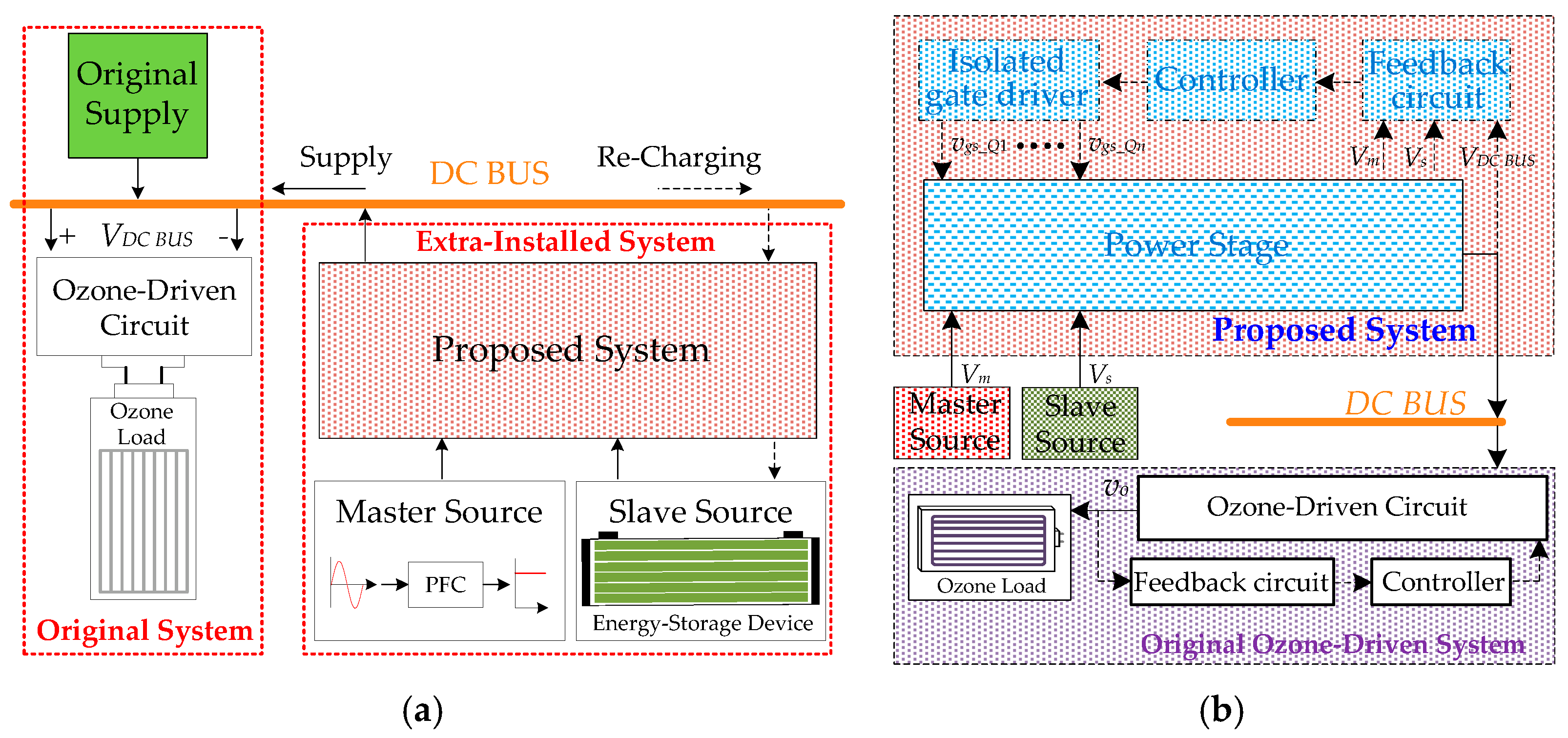
- The proposed modified-bridge circuit accomplished in this paper emphasizes the benefits of using two input power sources that are supplying coordinately to improve the supplied reliability and reduce the component cost for the ozone-driven system.
- (2)
- The proposed system can be extra-installed in the original ozone-driven system, which means that it is not necessary to replace the original one, keeping the ozone quality and reducing the replacement cost.
- (3)
- The resonant circuit design is of a symmetrical type, which achieves a similar resonant property under the bi-directional power transmission. Difficult control and a complicated algorithm are unnecessary to enhance the stability of the proposed system.
- (4)
- The voltage status of each port can be detected through the control system operation mode setting by judging whether the energy is being provided through DC BUS or re-charged to the slave source (energy storage device).
2. Operations of the Proposed System
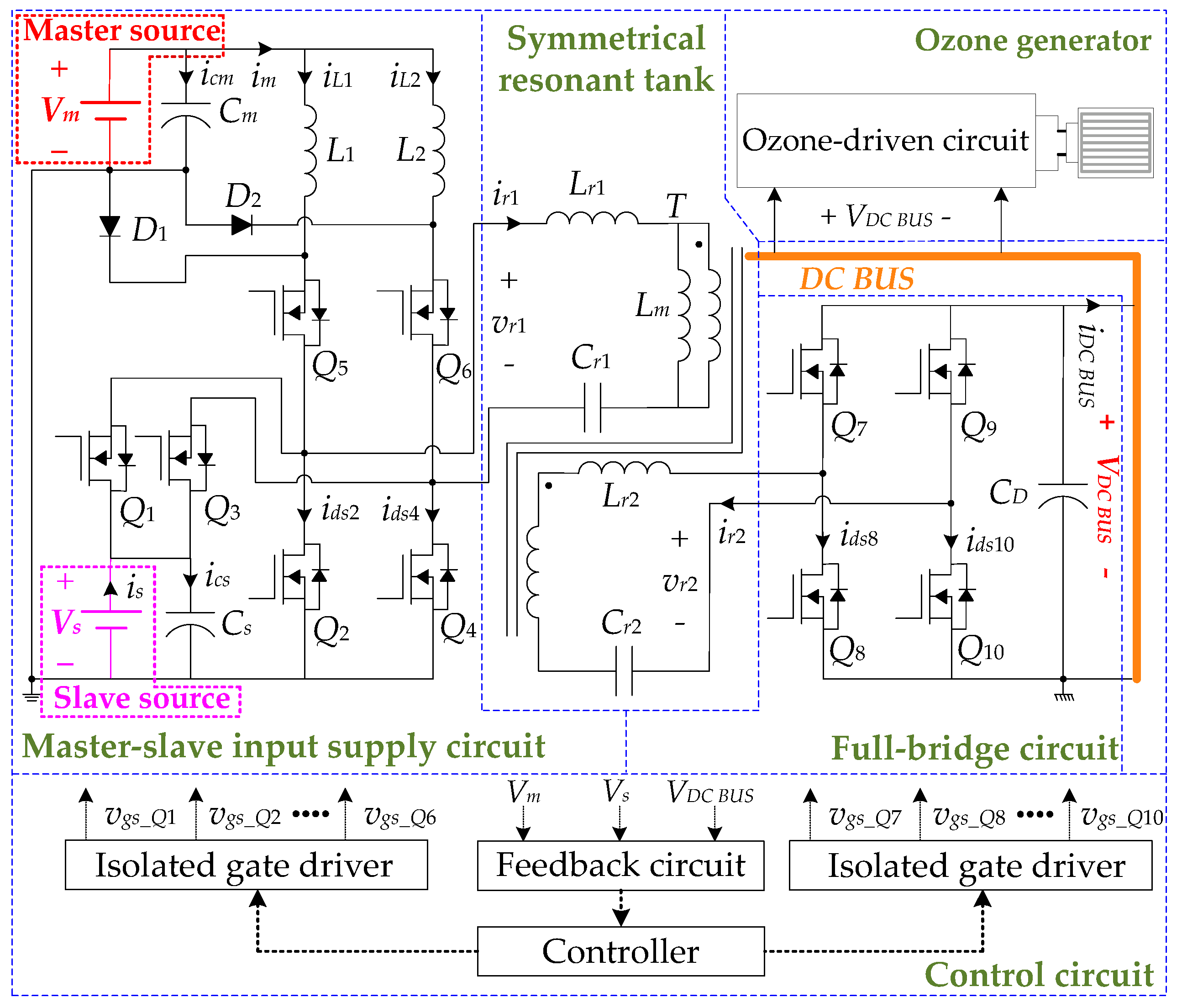
2.1. System and Circuit Description
2.2. Operation Mode and Circuit Analysis
- (1)
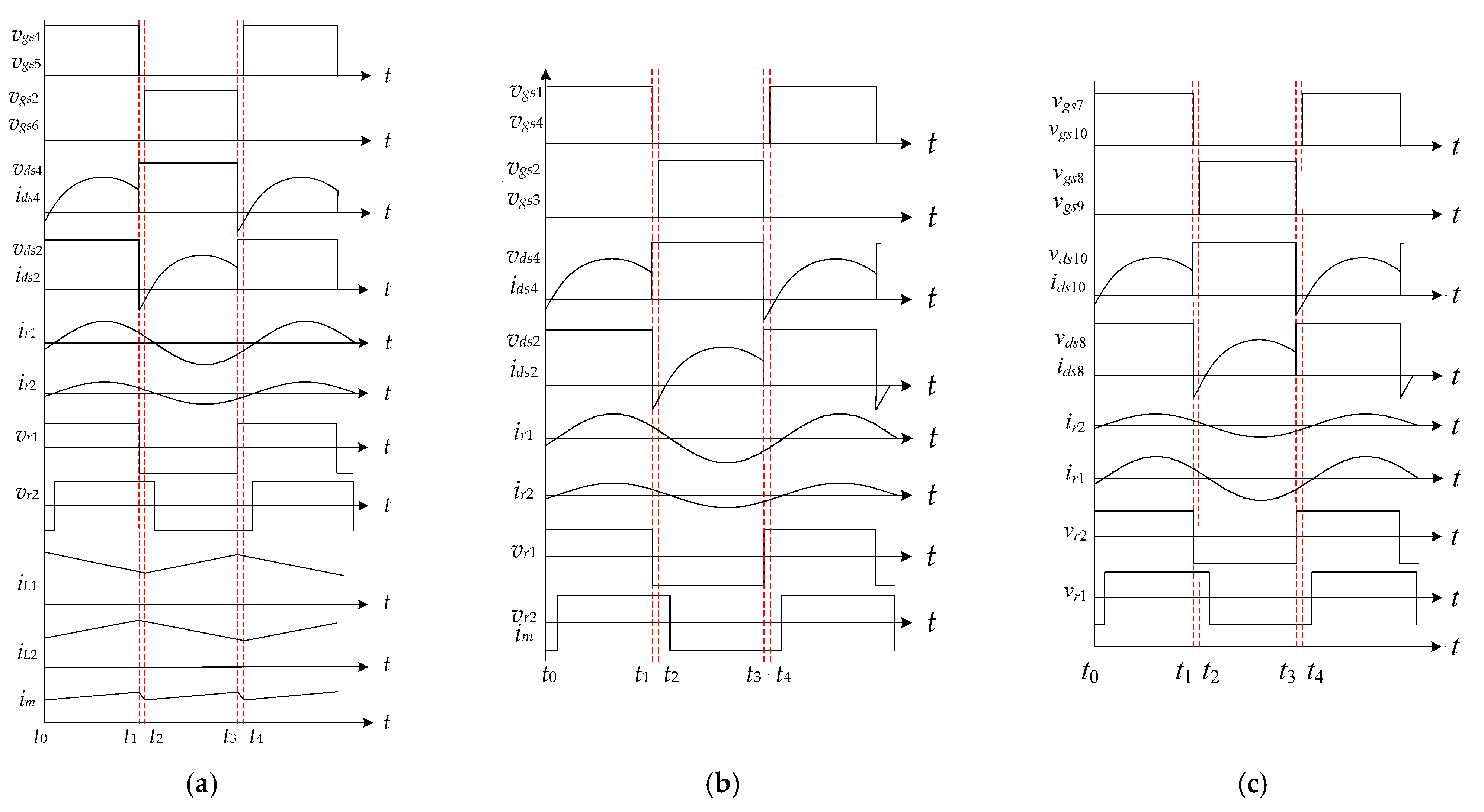
- Mode I (t0–t1): As shown in Figure 3a, Q2 and Q6 are turned off and Q4 and Q5 are turned on, achieving zero-voltage switching in this mode; the energy of the master source is stored in inductor L2 by turning on Q4 and releasing the energy of inductor L1, which is stored in the energy storage device and Cs by turning on Q5 and the diode of Q1. Therefore, the currents of L1 and L2 (iL1 and iL2) linearly decrease and increase, respectively. At this time, since the resonant voltage vr1 of the primary side is a positive square wave, the resonant current ir1 of the primary side flowing through Q1 and Q4 is positive and the resonant current ir2 of the secondary side flows through the body diode of Q7 and Q10 to transfer the energy to DC BUS with output capacitor CD. It is noted that the current im of the master source has low ripples because iL1 and iL2 are interleaved to store and release energy, which can contribute to mitigating the burden of the master source supply. This operation enters the next mode until Q4 and Q5 are turned off.
- (2)
- Mode II (t1–t2): In this mode, all power transistors Q1–Q6 are turned off, as shown in Figure 3b. The energy of L2 begins to be released and iL2 linearly decreases; thus, the energy of L2 is stored in the energy storage device and Cs through the body diode of Q3 and ir1 is freewheeling through the body diodes of Q2 and Q3 at the same time. When the voltage of the parasitic capacitor of Q2 and Q3 drops to zero, the body diodes of Q2 and Q3 provide a path for current freewheeling. Here, iL1 still decreases and iL2 begins to decrease. When Q2, Q3, and Q6 are turned on, this operation enters the next mode.
- (3)
- Mode III (t2–t3): As shown in Figure 3c, Q2 and Q6 are turned on and achieve zero-voltage switching in this mode. The energy of inductor L2 is charged to the energy storage device and Cs by turning on Q6 and the body diodes of Q3, and the energy of the master source is stored in inductor L1 by turning on Q2. Therefore, iL1 and iL2 linearly increase and decrease, respectively. Since the resonant voltage vr1 of the primary side becomes a negative square wave in this time, the current ir1 becomes negative and flows through Q2 and Q3. ir2 also becomes negative and flows through the body diode of Q8 and Q9 and transfers the energy to DC BUS with output capacitor CD. When Q2 and Q6 are turned off, this operation enters the next mode.
- (4)
- Mode IV (t3–t4): In this mode, all power transistors Q1–Q6 are turned off again, as shown in Figure 3d; the energy of L1 begins to be released; and iL1 linearly decreases. Thus, the energy of L1 is stored in the energy storage device and Cs through the body diode of Q1. Meanwhile, ir1 is freewheeling through the body diodes of Q1 and Q4. When the voltage of the parasitic capacitor of Q2 and Q3 drops to zero, the body diodes of Q1 and Q4 provide a path for current freewheeling. Here, iL1 begins to decrease and iL2 continues to decrease. When Q4 and Q5 are turned on again and the circuit returns to Mode I, the aforementioned mode of operation continues.
- (1)
- Mode I (t0–t1): As shown in Figure 4a, Q2 and Q3 are turned off, Q1 and Q4 are turned on, and the zero-voltage switching of Q1 and Q4 is achieved in this mode. Because Q5 and Q6 are always turned off in this mode, if there are surplus energies in these inductors (L1 and L2), iL1 and iL2 must be freewheeling through D1 and D2 until both iL1 and iL2 linearly decrease to zero. Since vr1 is a positive square wave, ir1 is also positive and flows through Q1 and Q4. The current ir2 flows through the body diode of Q7 and Q10, and the energy is transferred to DC BUS with output capacitor CD. This operation enters the next mode when Q1 and Q4 are turned off.
- (2)
- Mode II (t1–t2): As shown in Figure 4b, all power transistors Q1–Q6 are turned off. When the voltage of the parasitic capacitor of Q2 and Q3 drops to zero, the body diodes of Q2 and Q3 provide a path for current freewheeling. ir1 is still positive and freewheeling through the body diodes of Q2 and Q3. iL1 and iL2 are still freewheeling through D1 and D2 if there are surplus energies in L1 and L2. When Q2 and Q3 are turned on, this operation enters the next mode.
- (3)
- Mode III (t2–t3): As shown in Figure 4c, because the voltage of Q2 and Q3 drops to zero in the last mode, Q2 and Q3 are turned on in this mode and zero-voltage switching of Q2 and Q3 is achieved. Since vr1 becomes a negative square wave at this time, ir1 becomes negative and flows through Q2 and Q3; ir2 also becomes negative and flows through the body diode of Q8 and Q9 and transfers the energy to DC BUS with output capacitor CD. Because no load can consume the surplus energies of L1 and L2, both iL1 and iL2 linearly decrease slowly through D1 and D2. When Q2 and Q3 are turned off, this operation enters the next mode.
- (4)
- Mode IV (t3–t4): In this mode, all power transistors Q1–Q6 are turned off again, as shown in Figure 4d. When the voltage of parasitic capacitors of Q1 and Q4 drops to zero, the body diodes of Q1 and Q4 provide a path for current freewheeling. Therefore, ir1 is freewheeling through body diodes of Q1 and Q4 at this time. In addition, because no load can consume the surplus energies of L1 and L2, both iL1 and iL2 linearly decrease slowly through D1 and D2. When Q1 and Q4 are turned on again and the circuit returns to Mode I, the aforementioned modes of operation continue.
- (1)
- Mode I (t0–t1): As shown in Figure 5a, because the voltage of Q7 and Q10 drops to zero in the last mode, Q7 and Q10 are turned on and achieve the zero-voltage switching in this mode by turning off Q8 and Q9. The resonant voltage vr2 is a positive square wave because this voltage is converted by the switching of Q7 and Q10. The resonant current ir2 is positive and flowing through Q7 and Q10, and the resonant current ir1 that is induced by transformer T is also positive and flows through the body diode of Q1 and Q4 to transfer the energy to the energy storage device with capacitor Cs. This operation enters the next mode until Q7 and Q10 are turned off.
- (2)
- Mode II (t1–t2): As shown in Figure 5b, all power transistors Q7–Q10 are turned off because the voltage of the parasitic capacitor of Q8 and Q9 drops to zero. ir1 is freewheeling through the body diode of Q8 and Q9. When Q8 and Q9 are turned on, this operation enters the next mode.
- (3)
- Mode III (t2–t3): As shown in Figure 5c, because the voltage of Q8 and Q9 drops to zero in the previous mode, Q8 and Q9 are turned on in this mode and the zero-voltage switching of Q8 and Q9 is achieved. The resonant voltage vr2 becomes a negative square wave because this voltage is converted by switching Q8 and Q9. The resonant current ir2 is positive and flows through Q8 and Q9, and the resonant current ir1 that is induced by transformer T is also positive and flows through the body diode of Q2 and Q3 to transfer the energy to the energy storage device with capacitor Cs. This operation enters the next mode until Q8 and Q9 are turned off.
- (4)
- Mode IV (t3–t4): In this mode, all power transistors Q7–Q10 are turned off, as shown in Figure 5d, because the voltage of the parasitic capacitor of Q7 and Q10 drops to zero. ir1 is freewheeling through the body diode of Q7 and Q10. When Q7 and Q10 are turned on again, the circuit returns to Mode I for the aforementioned cycle to continue.
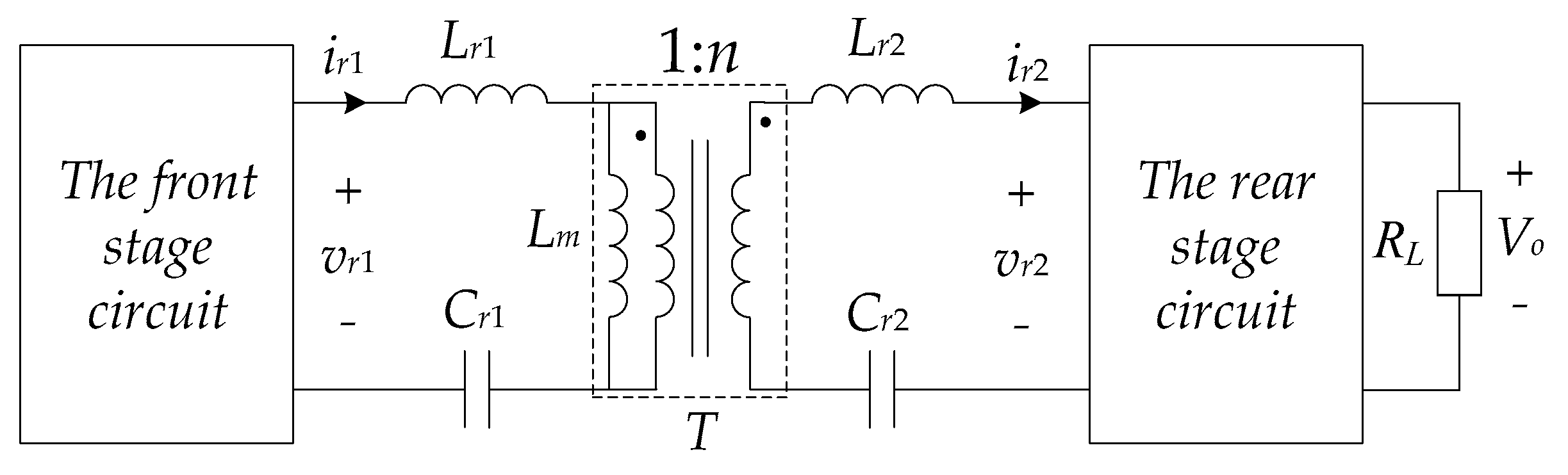
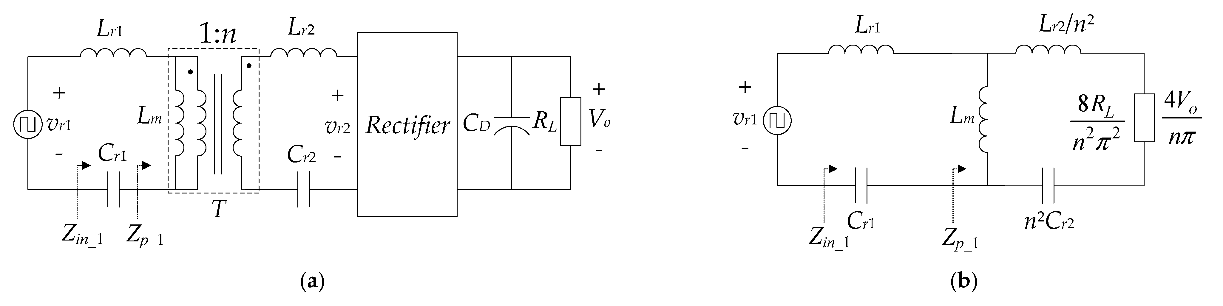
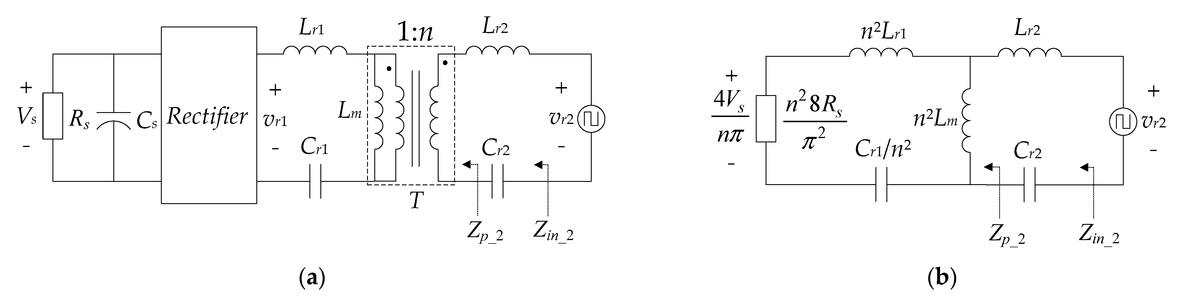
3. Symmetrical Resonant Circuit Analysis
3.1. Operation Mode and Circuit Analysis
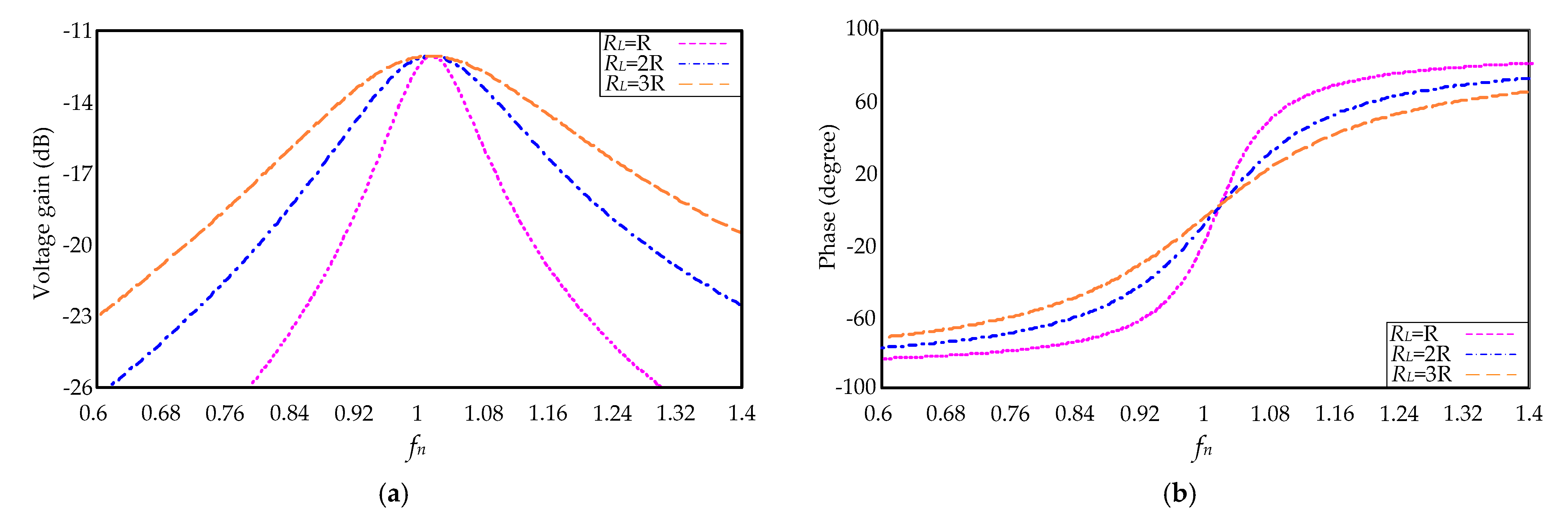
3.2. Analysis of Voltage Gain and Impedance Phase
3.2.1. The Energy Is Provided by the Master or the Slave Source
3.2.2. The Energy Is Provided from DC BUS
4. Control Mechanism Analysis
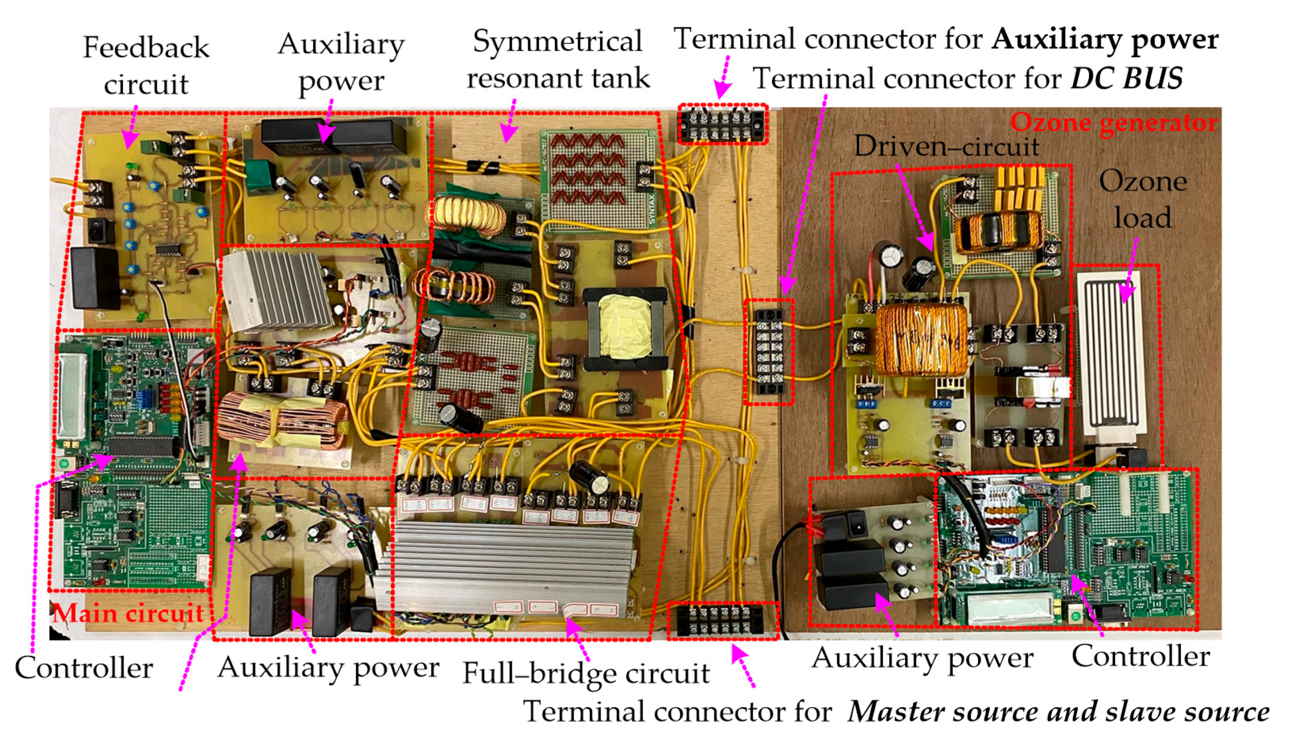
5. Experimental Results
5.1. Input and Output Status
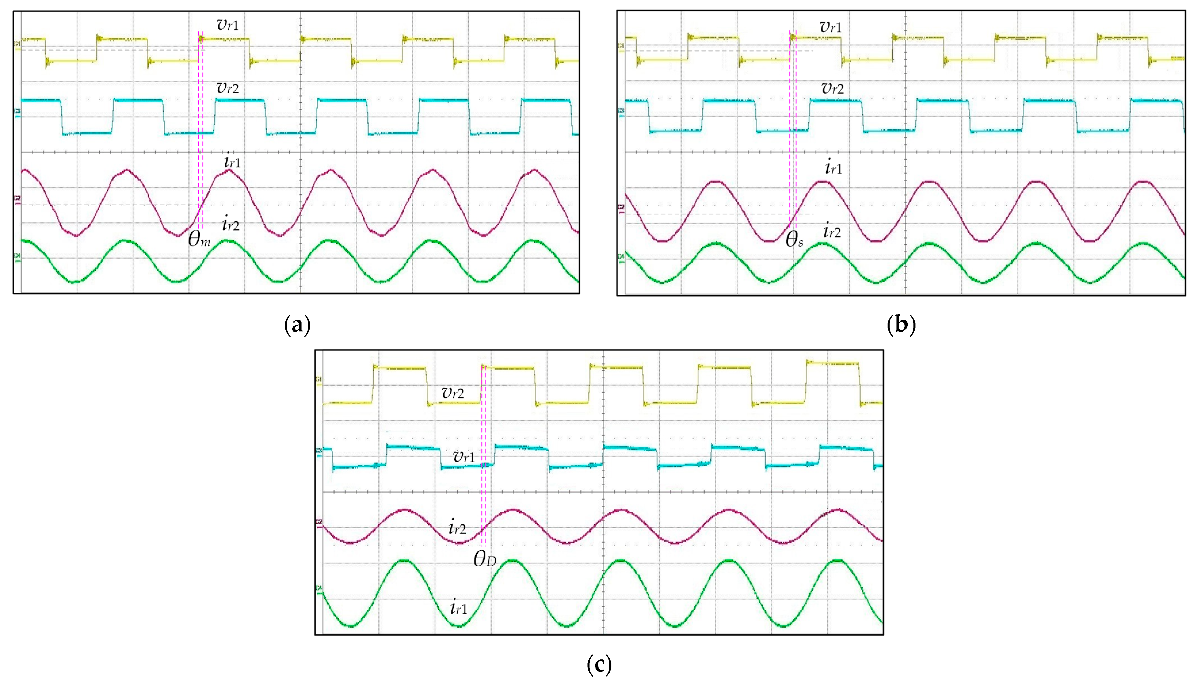
5.2. Resonant Property Verification
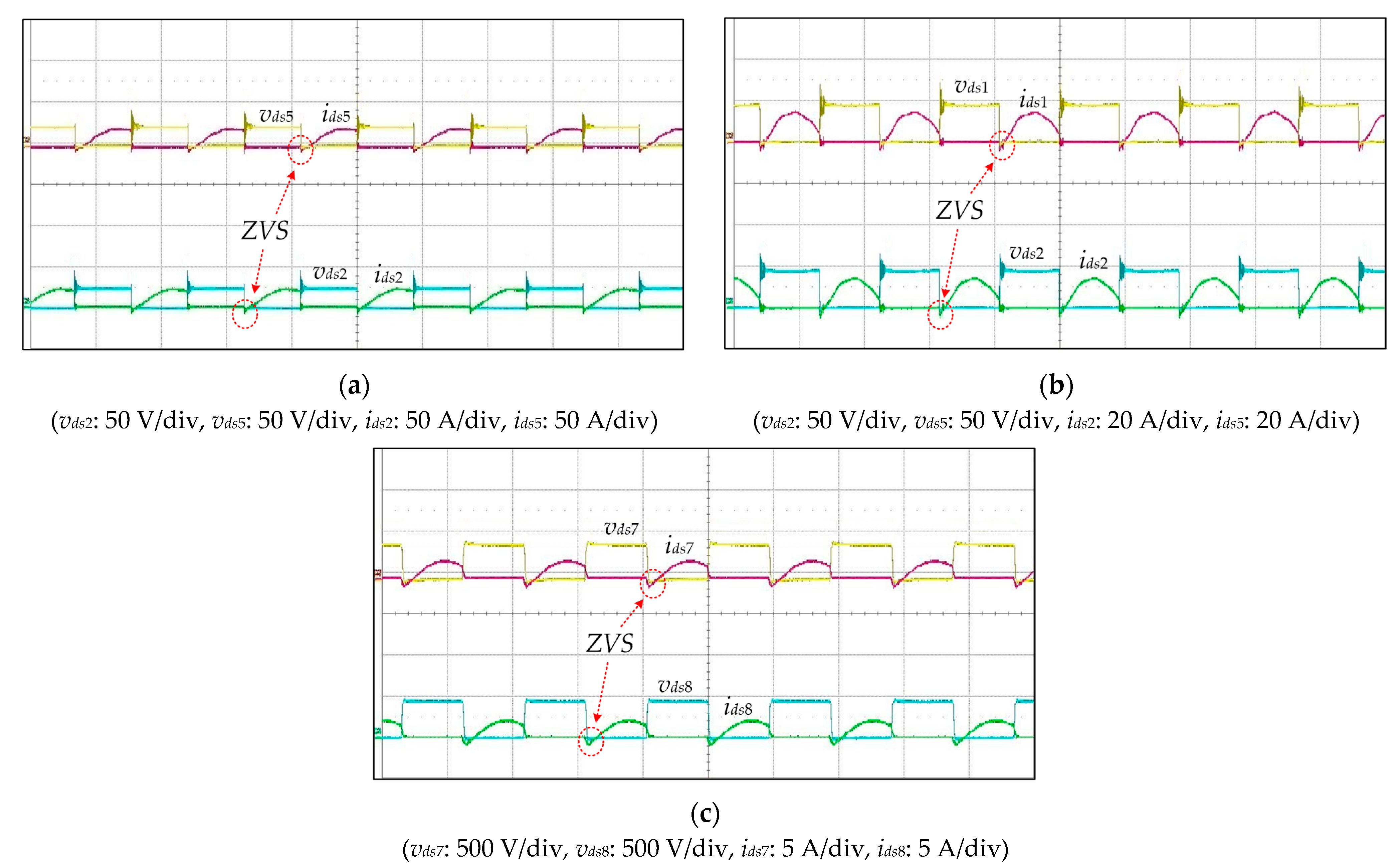
5.3. Zero-Voltage Switching Verification
5.4. Operation Mode Change Verification
5.5. Comparison with the References
6. Conclusions
Author Contributions
Funding
Acknowledgments
Conflicts of Interest
References
- Mitsugi, F. Practical Ozone Disinfection of Soil via Surface Barrier Discharge to Control Scab Diseases on Radishes. IEEE Trans. Plasma Sci. 2019, 47, 52–56. [Google Scholar] [CrossRef]
- Mitsugi, F.; Ebihara, K.; Horibe, N.; Aoqui, S.; Nagahama, K. Practical Soil Treatment in a Greenhouse Using Surface Barrier Discharge Ozone Generator. IEEE Trans. Plasma Sci. 2017, 45, 3082–3088. [Google Scholar] [CrossRef]
- Mitsugi, F.; Abiru, T.; Ikegami, T.; Ebihara, K.; Nagahama, K. Treatment of Nematode in Soil Using Surface Barrier Discharge Ozone Generator. IEEE Trans. Plasma Sci. 2017, 45, 3076–3081. [Google Scholar] [CrossRef]
- Yang, L.; Wang, X.Y.; Zhu, D.; Zhang, Q.; Xi, T.; Liu, D.P.; Niu, J.H.; Xi, T.; Zhao, Y.; Qi, Z.H.; et al. Mechanism of Amoxicillin Degradation in Water Treated by Atmospheric-Pressure Air Microplasma. IEEE Trans. Plasma Sci. 2020, 48, 953–960. [Google Scholar] [CrossRef]
- Abkenar, P.P.; Iman-Eini, H.; Samimi, M.H.; Emaneini, M. Design and Implementation of Ozone Production Power Supply for the Application of Microbial Purification of Water. IEEE Trans. Power Electron. 2020, 35, 8215–8223. [Google Scholar] [CrossRef]
- Kuwahara, T. Reduction in Energy Consumption Using Fuel Cells in Nonthermal Plasma-Based Water Sterilization by Bubbling Ozone. IEEE Trans. Ind. Appl. 2018, 54, 6414–6421. [Google Scholar] [CrossRef]
- Liu, C.; Nishida, Y.; Iwasaki, K.; Sung, W.; Wu, F. Characteristics of DC or Pulsed-Type High-Electric Field Plasma and its Application to Air Cleaning System. IEEE Trans. Plasma Sci. 2019, 47, 1121–1128. [Google Scholar] [CrossRef]
- Okubo, M.; Hiroyasu, Y.; Kuroki, T. Ion Cluster Formation by Nonthermal Plasma Induced by Pulse Corona Discharge Toward Indoor Air Cleaning. IEEE Trans. Ind. Appl. 2020, 56, 5480–5488. [Google Scholar] [CrossRef]
- Tong, Z.; Ding, P.; Su, Y.; Niu, J.; Wang, D.; Jin, Z. Surface Improvement of InAlAs/InGaAs InP-Based HEMT Through Treatments of UV/Ozone and TMAH. IEEE J. Electron. Devices Soc. 2020, 8, 600–607. [Google Scholar] [CrossRef]
- Nascimento, F.; Machida, M.; Canesqui, M.A.; Moshkalev, S.A. Comparison between Conventional and Transferred DBD Plasma Jets for Processing of PDMS Surfaces. IEEE Trans. Plasma Sci. 2017, 45, 346–355. [Google Scholar] [CrossRef] [Green Version]
- Wu, Q.F.; Wang, M.G.; Zhou, W.Y.; Wang, X.M.; Liu, G.L.; You, C.Q. Analytical Switching Model of a 1200V SiC MOSFET in a High-Frequency Series Resonant Pulsed Power Converter for Plasma Generation. IEEE Access. 2019, 7, 99622–99632. [Google Scholar] [CrossRef]
- Park, S.H.; Sohn, Y.H.; Cho, G.H. SiC-Based 4 MHz 10 kW ZVS Inverter with Fast Resonance Frequency Tracking Control for High-Density Plasma Generators. IEEE Trans. Power Electron. 2020, 35, 3266–3275. [Google Scholar] [CrossRef]
- Azizi, M.; van Oorschot, J.J.; Huiskamp, T. Ultrafast Switching of SiC MOSFETs for High-Voltage Pulsed-Power Circuits. IEEE Trans. Plasma Sci. 2020, 48, 4262–4272. [Google Scholar] [CrossRef]
- Pang, L.; Long, T.J.; He, K.; Huang, Y.R.; Zhang, Q.G. A Compact Series-Connected SiC MOSFETs Module and Its Application in High Voltage Nanosecond Pulse Generator. IEEE Trans. Power Electron. 2019, 66, 9238–9247. [Google Scholar] [CrossRef]
- Jafari, H.; Habibi, M. High-Voltage Charging Power Supply Based on an LCC-Type Resonant Converter Operating at Continuous Conduction Mode. IEEE Trans. Power Electron. 2020, 35, 5461–5478. [Google Scholar] [CrossRef]
- Ta, L.A.D.; Dao, N.D.; Lee, D.C. High-Efficiency Hybrid LLC Resonant Converter for On-Board Chargers of Plug-In Electric Vehicles. IEEE Trans. Power Electron. 2020, 35, 8324–8334. [Google Scholar] [CrossRef]
- Lin, R.L.; Huang, L.H. Efficiency Improvement on LLC Resonant Converter Using Integrated LCLC Resonant Transformer. IEEE Trans. Ind. Appl. 2018, 54, 1756–1764. [Google Scholar] [CrossRef]
- Fei, C.; Li, Q.; Lee, F.C. Digital Implementation of Light-Load Efficiency Improvement for High-Frequency LLC Converters with Simplified Optimal Trajectory Control. IEEE Trans. Emerg. Sel. Top. Power Electron. 2018, 6, 1850–1859. [Google Scholar] [CrossRef]
- Saleh, S.A.; Allen, B.; Ozkop, E.; Colpitts, B.G. Multistage and Multilevel Power Electronic Converter-Based Power Supply for Plasma DBD Devices. IEEE Trans. Ind. Electron. 2018, 65, 5466–5475. [Google Scholar] [CrossRef]
- Kurm, S.; Agarwal, V. Hybrid Energy Storage System Based on a Novel Reduced Rating Multi-Input Converter. IEEE Trans. Power Electron. 2020, 35, 12133–12142. [Google Scholar] [CrossRef]
- Biswas, I.; Kastha, D.; Bajpai, P. Small Signal Modeling and Decoupled Controller Design for a Triple Active Bridge Multiport DC–DC Converter. IEEE Trans. Power Electron. 2021, 36, 1856–1869. [Google Scholar] [CrossRef]
- Karthikeyan, V.; Gupta, R. Multiple-Input Configuration of Isolated Bidirectional DC-DC Converter for Power Flow Control in Combinational Battery Storage. IEEE Trans. Ind. Informat. 2018, 14, 2–11. [Google Scholar] [CrossRef]
- Mohammadi, M.R. An Active-Clamping ZVS Interleaved Buck/Boost Bidirectional Converter with One Auxiliary Switch. IEEE Trans. Ind. Electron. 2020, 67, 7430–7438. [Google Scholar] [CrossRef]
- Pajnić, M.; Pejović, P. Zero-Voltage Switching Control of an Interleaved Bi-Directional Buck-Boost Converter with Variable Coupled Inductor. IEEE Trans. Power Electron. 2019, 34, 9562–9572. [Google Scholar] [CrossRef]
- Zhang, C.J.; Li, P.C.; Kan, Z.Z.; Chai, X.H.; Guo, X.Q. Integrated Half-Bridge CLLC Bidirectional Converter for Energy Storage Systems. IEEE Trans. Ind. Electron. 2018, 65, 3879–3889. [Google Scholar] [CrossRef]
- Zhao, B.; Zhang, X.; Huang, J.J. AI Algorithm-Based Two-Stage Optimal Design Methodology of High-Efficiency CLLC Resonant Converters for the Hybrid AC–DC Microgrid Applications. IEEE Trans. Ind. Electron. 2019, 66, 9756–9767. [Google Scholar] [CrossRef]
- Min, J.; Ordonez, M. Bidirectional Resonant CLLC Charger for Wide Battery Voltage Range: Asymmetric Parameters Methodology. IEEE Trans. Power Electron. 2021, 36, 6662–6673. [Google Scholar] [CrossRef]
- Lee, M.; Lai, J.S. Spread-Spectrum Frequency Modulation with Adaptive Three-Level Current Scheme to Improve EMI and Efficiency of Three-Level Boost DCM PFC. IEEE Trans. Power Electron. 2021, 36, 2476–2480. [Google Scholar] [CrossRef]
- Wu, H.; Zhang, Y.; Jia, Y. Three-Port Bridgeless PFC-Based Quasi Single-Stage Single-Phase AC–DC Converters for Wide Voltage Range Applications. IEEE Trans. Ind. Electron. 2018, 65, 5518–5528. [Google Scholar] [CrossRef]
- Mahmoodsaleh, M.; Adib, E. Soft-Switching Bridgeless Buck-Boost PFC Converter Using Single Magnetic Core. IEEE Trans. Ind. Electron. 2021, 68, 5704–5711. [Google Scholar] [CrossRef]
- Qi, W.L.; Li, S.N.; Yuan, H.W.; Tan, S.C.; Hui, S.Y. High-Power-Density Single-Phase Three-Level Flying-Capacitor Buck PFC Rectifier. IEEE Trans. Power Electron. 2019, 34, 10833–10844. [Google Scholar] [CrossRef]
- Hosseinabadi, F.; Adib, E.; Tehrani, B.M. A Soft-Switching Step-Down PFC Converter with High Power Factor Using Auxiliary Flyback Circuit. IEEE Trans. Ind. Electron. 2019, 66, 6887–6894. [Google Scholar] [CrossRef]
- Sharifi, S.; Monfared, M.; Babaei, M. Ferdowsi Rectifiers—Single-Phase Buck-Boost Bridgeless PFC Rectifiers with Low Semiconductor Count. IEEE Trans. Ind. Electron. 2020, 67, 9206–9214. [Google Scholar] [CrossRef]


| No. | Features | Reference |
|---|---|---|
| [11] | An accurate analytical converter-level model is introduced. The model evaluates and optimizes the switching solution of a SiC MOSFET for the pulsed power converter. | SiC MOSFET application of the ozone-driven circuit design for increasing the component reliability |
| [12] | A high-power high-frequency ICP drive system that achieves high efficiency and durability is proposed. A 10 kW 4 MHz switching inverter and a novel control method are proposed for ICP with a high Q factor and highly variable impedance. The proposed phase lead sensing circuit can always guarantee ZVS operation of a high-power high-frequency switching inverter. Through the proposed system, ICP with a much higher plasma density can be safely driven. | |
| [13] | An optimized version of a gate-boosting driver circuit for SiC MOSFETs for ultrafast switching is proposed. A MOSFET turn-on time of below 2 ns is achievable at a high operating voltage and moderate current and below 3 ns for a wider range of load-current and operating voltage conditions. | |
| [14] | A high-voltage SiC MOSFETs module can serve as the main switch in a repetitive high-voltage nanosecond pulse generator. A series-connected MOSFETs module with only a single external gate driver requiring few components is suitable for a compact assembly. A 10 kV SiC MOSFETs module with a turn-on transition time ~10 ns is developed. A compact and high-voltage pulse generator composed of three 10 kV SiC MOSFETs module is tailored, with a typical rise time of ~40 ns and peak a voltage of ~30 kV. | |
| [15] | A 2.0 kW high-voltage rep-rate charging power supply based on a non-isolated inductor–capacitor–capacitor (LCC)-type resonant converter operating in continuous conduction mode is proposed. It provides a constant charging current with high control accuracy/efficiency. The design of the proposed capacitor charging power supply (CCPS) is a low-cost, simpler, compact, and efficient driver for the miniature pulsed plasma sources. | Different resonant architecture analysis for acquiring a higher voltage gain |
| [16] | A hybrid LLC resonant converter design is proposed. There are three modes of operation: As a full-bridge converter, as a dual-phase half-bridge LLC converter, or as a single-phase half-bridge LLC converter. Using GaN devices with a power density of 65 W/in 3 has been designed. | |
| [17] | A comparative half-bridge LLC resonant converter using the integrated LCLC resonant transformer is proposed. To reduce the demanded leakage inductance, a resonant capacitor can be connected in parallel to the magnetizing inductor through auxiliary winding as an LCLC resonant transformer. An integrated LCLC resonant transformer with lower leakage inductance for efficiency comparison is implemented. | |
| [18] | The light-load efficiency of the LLC resonant converters is an improvement. The simplified optimal trajectory control (SOTC) for burst mode can solve this issue by using an optimal switching pattern for burst-on time. The digital implementation of SOTC for burst mode and its limitation in a high-frequency LLC converter are discussed. | |
| [19] | Multistage and multilevel switch-mode converters are employed to construct the power supply. The proposed MSML-PEC power supply uses boost dc-dc PECs without high-frequency transformers. The removal of high-frequency transformers has improved the average efficiency and reduced the size of each dc-dc PEC. Modular, lightweight, and compact size power supply has been achieved. | Multiple input design for adding the input port to increase the supply reliability |
| [20] | A novel multi-input converter (MIC) is proposed in this article for interfacing a battery-SC combination. The SC converter is mostly rated for the full surge power. The battery is operated in current control mode under normal loading conditions. The proposed system balances the flow of power between the load and the HESS. | |
| [21] | Modeling and two controller design techniques for a triple active bridge (TAB) three-port dc-dc converter comprising the fuel cell, the battery, and the load are proposed. A new decoupling matrix-based proportional-integral controller design method reduces the design complexity and improves the system dynamic performance in comparison to similar three-port converters reported in the paper. | |
| [22] | A multiple-input configuration of an isolated bidirectional dual-active bridge dc-dc converter (MIBDC) is proposed for power flow control in a combinational battery storage. The proposed system can be operated in an independent source or a combinational source mode of operation to control the power transfer. It has the capability of bidirectional power flow and smoother transition. The proposed configuration can also be used with unequal voltage level sources by connecting them in series on the multi-input side. | |
| [23] | A ZVS interleaved buck/boost bidirectional converter using the active-clamp technique is introduced in this paper. Applying a simple auxiliary circuit comprised of an auxiliary switch, an auxiliary inductor, and a clamp capacitor, ZVS condition is achieved by the converter operating duty cycle or load condition. The converter can operate with the conventional fixed-frequency pulse-width modulation (PWM) control. | Bidirectional converters and symmetrical resonant circuit discussion for delivering and re-charging of energy regulation |
| [24] | An interleaved bi-directional buck-boost is proposed for achieving zero-voltage switching. Applying a coupled inductor with a variable coupling coefficient achieves a wide input–output voltage operating range. The variable coupled inductor significantly improves the soft-switching range and reduces the circulating energy.The gallium nitride interleaved bi-directional buck-boost converter is applied in this paper. | |
| [25] | An integrated half-bridge CLLC (IHBCLLC) resonant bidirectional dc-dc converter is proposed in various applications, including energy-storage systems. A half-bridge CLLC resonant circuit and a buck/boost circuit are integrated. The proposed converter obtains the high voltage gain by pulse-width modulation. The CLLC resonant circuit can help MOSFETs to achieve soft switching and high voltage gain. | |
| [26] | The total power loss optimization and the magnetic design of the CLLC resonant converter based on the artificial intelligence (AI) algorithm are proposed in this paper. The parameters of the magnetic component and the resonant component are derived by the AI algorithm. The parameters of the transformer are optimized by the AI algorithm. A planar transformer is used for CLLC designing in this paper. | |
| [27] | The CLLC bidirectional resonant converter is discussed in this paper. Application fields are battery chargers and dc microgrids. Asymmetric parameters methodology (APM) can design gain curves for charging and discharging modes separately. |
| Specifications | Title 3 |
|---|---|
| Master input source voltage, Vm | 48 V |
| Slave input source voltage, Vs | 40 V–54.6 V |
| Output voltage, Vo | 400 V |
| Power transistors, Q1–Q10 | IXFH44N50P |
| Storage inductors, L1 and L2 | 1.21 mH |
| Capacitors of the master source and the slave source, Cm and Cs | 470 μF/100 V |
| Output capacitors, CD | 470 μF/450 V |
| Maximum output current, Io | 2 A |
| Maximum output power, Po | 800 W |
| Items | Values |
|---|---|
| Resonant frequency | 55 kHz |
| Resonant inductor of the primary side (Lr1) | 124.8 uH |
| Resonant capacitor of the primary side (Cr1) | 67.1 nF |
| Magnetic inductor (Lm) | 2.75 mH |
| Resonant inductor of the secondary side (Lr2) | 2.034 mH |
| Resonant capacitor of the secondary side (Cr2) | 4.12 nF |
| Paper No. | Input Port Amount | Used Circuit Amount | Supply Coordination Function | Input Voltage | Output Voltage |
|---|---|---|---|---|---|
| [11] | 1 | 1 | No | 400 VDC | 8.2 kV |
| [12] | 1 | 1 | No | 208 VAC | NA |
| [13] | 1 | 1 | No | 1200 VDC | 1.6 kV |
| [14] | 1 | 1 | No | NA | 10–30 kV |
| [15] | 1 | 1 | No | 60 VDC | 20 kV |
| [19] | 5 | 6 | No | 30 VDC | 1500 V |
| ✓ The proposed system | 2 | 1 | Yes | Master: 48 VDC Slave: 40~54.6 VDC | 400 V |
Publisher’s Note: MDPI stays neutral with regard to jurisdictional claims in published maps and institutional affiliations. |
© 2022 by the authors. Licensee MDPI, Basel, Switzerland. This article is an open access article distributed under the terms and conditions of the Creative Commons Attribution (CC BY) license (https://creativecommons.org/licenses/by/4.0/).
Share and Cite
Hung, T.-C.; Lee, T.-S.; Huang, K.-C.; Chen, Y.-H. Design of a Modified-Bridge Circuit with a Master-Slave Input Supply Mechanism for Ozone-Driven System Applications. Electronics 2022, 11, 254. https://doi.org/10.3390/electronics11020254
Hung T-C, Lee T-S, Huang K-C, Chen Y-H. Design of a Modified-Bridge Circuit with a Master-Slave Input Supply Mechanism for Ozone-Driven System Applications. Electronics. 2022; 11(2):254. https://doi.org/10.3390/electronics11020254
Chicago/Turabian StyleHung, Te-Chun, Tsong-Shing Lee, Kuan-Chieh Huang, and Yu-Hsiang Chen. 2022. "Design of a Modified-Bridge Circuit with a Master-Slave Input Supply Mechanism for Ozone-Driven System Applications" Electronics 11, no. 2: 254. https://doi.org/10.3390/electronics11020254