Abstract
Ka-band frequencies are becoming increasingly popular due to their application potential in high-data-rate wireless communications relevant to 5G applications, satellite link establishment, etc. High-power amplifiers in this frequency band, offering several tens of watts of output RF power, are one of the main enabling components of these communication systems. This article reports the design studies and analysis of the radio frequency (RF) section of a multiple beam-extended interaction klystron (MB-EIK). The proposed multiple beam RF section with a ladder-type EIK structure offers several crucial features, such as a low-voltage operation, moderate operational bandwidth, and high output power. Starting from the design of the intermediate cavities, the input and output sections and the overall RF section are presented. The proposed RF section supports the operation at 28.5 GHz center frequency with about a 500 MHz 3 dB bandwidth employing four electron beams with a 4 kV DC accelerating field.
1. Introduction
Conventional klystrons are single-beam amplifiers where only one electron beam is employed for the RF amplification [1,2,3]. In single-beam klystrons, generally with a low-to-medium perveance, a high-voltage beam is used to obtain a high output power. In these cases, obtaining a higher output power is constrained by the possibilities of the voltage breakdown—in the electron gun region or the RF section. The usage of a very high perveance and the low-voltage electron beam is not a feasible option for obtaining a higher power. This will demand a very high magnetic field for focusing the electron beam.
These reasons necessitate the use of multiple beam klystrons (MBKs), in which multiple numbers of electron beams are used. In these devices, the currents of the individual beams and the operating voltage are not high, but the total current of the device becomes high [4].
Although there are several attractive features of the MBKs, the design of these devices is challenging. The main components of the MBK, i.e., the electron gun, focusing scheme, RF interaction structure with appropriate input/output sections, etc., require meticulous design and optimization. The design of the RF interaction structure, which mainly dictates the interaction between the electron beam and the RF wave, is one of the challenging tasks. The RF cavities with a high shunt impedance are required for an effective beam–wave interaction. In the case of MBKs (or any other type of klystrons) operating at higher frequencies, achieving higher shunt impedances in the gain cavities and symmetric coupling in the input/output cavities is challenging. One of the ways to increase the shunt impedance of the RF cavities is to use the extended interaction type of cavities [5,6,7,8,9]
Klystrons with extended interaction RF cavities (EIKs) are designed with multiple gaps to achieve larger shunt impedances for an efficient beam–wave energy transfer and the proper synchronization of the electron beam with the RF field [10,11,12,13,14].
The MBKs with microfabrication-compatible extended interaction cavities, a lower operating voltage, and a (few hundred mA) beam current can provide a moderate operating bandwidth and RF output power in Ka-band frequencies. These characteristics offer cherished alternatives to solid-state-based RF amplifiers in this frequency range, which may be applied for long-distance high-data-rate wireless communications, such as 5G wireless back-haul/front-haul, wireless middle-mile connectivity reconfigurable 5G deployments, etc. Because the usage of these amplifiers enables achieving a high data rate without the deployment of fibers, it is suitable for difficult terrains and/or sparsely located rural populations where fiber laying is commercially not viable [15,16].
In this work, we report a compact, low-voltage-operated (~4kV) MBK employing a microfabrication-compatible novel ladder-type interaction structure operating at a 28.5 GHz frequency. An axial magnetic field of 0.35T is employed for focusing the electron beams, and a 500 MHz (−3 dB) bandwidth has been obtained, with a peak power level of 375 W. Some other klystrons (single beam or multiple beams) reported in this frequency band offer higher output powers—but the operating voltages are higher (9.5 kV to 500 kV), form factors are larger, and offered bandwidths are less [17,18,19].
Although the estimated bandwidth of the device is less than that of the traveling wave tubes operating in these frequency bands, the lower operating voltage and relatively simple (than the TWTs) fabrication possibilities make these devices attractive for high-data-rate communication applications [20,21].
In comparison with the state-of-the-art semiconductor power amplifiers, the output power and efficiency of the proposed device are far superior, but the available bandwidth is less. Although there have been remarkable advancements in the solid-state technology in recent times (especially the GaN technology), the output power level provided by a single microwave monolithic integrated circuit (MMIC) around 28 GHz is still limited to around 16 watts (Max). The output power level of about 100 W with an efficiency of 19% can be achieved using power-combining techniques [22,23].
Besides the communication applications, a similar concept may be adopted to design the devices operating in other frequency bands and/or power levels. The applications of such devices include particle accelerators, industrial and plasma heating, RADARs and active denial technologies, deep space communication, etc. [24,25,26,27,28]. A number of amplifiers and oscillators operating in the Ka-Band and other higher-frequency bands employing multiple beams and extended interaction structures are being explored globally [19,29,30,31,32,33].
The arrangement of this paper is as follows: In Section 1, a short introduction of multiple beam klystrons and their application scopes are stated; the design approach of the RF section of the proposed ladder-type multibeam EIK is provided in Section 2; in Section 3, the simulation results of the intermediate cavities, input/output cavities, and beam–wave interaction are presented; and the conclusion of this work is given in Section 4, followed by the references.
2. Design Approach
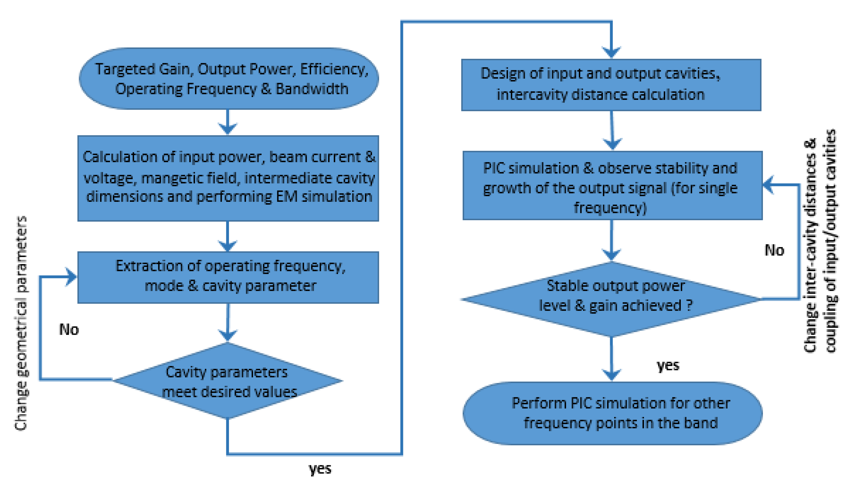
The targeted design specification of the proposed multiple beam klystron is given in Table 1. Targeted nominal bandwidth has been taken as 500 MHz because similar bandwidths are being considered for 5G systems envisaged in the Ka-band frequency range. The total beam current (therefore individual current of beamlets) has been kept in a range such that the required focusing magnetic field can be obtained by using permanent magnets, therefore avoiding complexity and requirement for magnet power supply. RF performance of a klystron, such as its gain, bandwidth, efficiency, etc., depends on the RF section’s design. Because the RF section is an ensemble of RF cavities joined together by the drift tubes at particular distances, the design of the RF section involves the extraction of RF cavity parameters and the drift tube dimensions. The approach followed for design of the proposed device is given in Figure 1.

Table 1.
Design specification of proposed multiple beam klystron.

Figure 1.
Flowchart of RF section design procedure.
The energy exchange between the accelerated electron beam and the RF signal takes place at the cavity gap. There are conflicting requirements in deciding the gap diameter and spacing. For efficient beam–wave interaction, both parameters should be small compared with electron transit time through the gap. However, very small gap diameter imposes severe complications in electron gun and magnetic focusing system design. Moreover, the small gap spacing increases the gap capacitance resulting in a reduced gain-bandwidth product. For small gap spacings, there are possibilities of voltage breakdown and resultant beam loss. Therefore, both parameters are optimized to achieve a compromised value of the same, keeping the set specification in mind. Moreover, proper coupling irises (or loops) are required for input and output cavities so that the device will have good matching at the input to the RF driver to the load at the output port. The analytical approach [24,25,27,34,35] used for designing for expression required to design the RF section is presented in the following section.
Ladder-shaped resonant cavities have been considered for larger shunt impedances (with extended interaction configuration), and multiple numbers of beams have been considered for low operating voltage (and individual beamlet current) and microfabrication and 3D fabrication compatibility. Initial cavity dimensions (height and width) have been determined using the conventional analytical formula [11,25,27,35,36,37,38].
where resonant frequency is denoted by fmm of TEmn or TMmn mode of a resonator with sides a and b. Light velocity in free space is represented by c. The relative permeability and permittivity of the medium are represented by µr and εr. It may be noted that TM mode has been considered where the electric field inside the gaps does not vary much in the beam propagation direction. For efficient RF amplification in the extended interaction cavity, different configurations of the operating mode are possible. Among these modes, the 2π mode of operation has been focused on because this mode generally provides maximum coupling between the RF signal and beam. The pitch length (p) and gap length (G) of the EIK cavities can be obtained using the Floquet theorem of periodicity. Phase velocity vp of the space harmonics is presented by
where ω = angular frequency, βe = Beam propagation constant. Considering length of the pitch as p and 2π mode of operation, one may have
Length of the gap (G) may be determined using the relation
and considering a gap transit angle (θ) of 1.5 radian. Initial dimensions of the RF section have been determined using the following conventional analytical formulae. When electrons are accelerated by DC voltage V0 before entering the input cavity is called DC electrons velocity (U0) in m/s
where e = charge of electron = 1.602 × 10⁻¹⁹ C and m = mass of electron = 9.109 × 10⁻³¹ kg. Angular frequency (ω) may be determined using the relation
where f is the linear frequency. Electron wave number (k) and drift tube radius (a) may be determined using the relation
The beam radius (b) can be determined using a beam fill factor of 70%, which is conventionally of the drift tube radius (a) for proper beam transmission through the drift section without interception. Therefore,
and charge density
If the electron beam continues beyond the axial position (λp), the electrons would continue to oscillate. The frequency at which they would oscillate is the electron plasma frequency (ωp).
where ε0 = 8.854 × 10⁻¹² farad/m and (e/m) = 1.758 × 10¹¹ C/kg. The equation shows that the plasma frequency is a function of the density of electron beam and DC velocity of the electrons. The reduced plasma frequency ωq is given by the expression
where R = 0.36784 is the plasma reduction factor. R can be found from standard curves or table. The reduced plasma wavelength (λq) and drift tube length (L) can be calculated as
The magnetic field, which exactly balances the space-charge force of the electrons, is called the Brillouin field. The resulting electron motion immersed in Brillouin field in form of a smooth rotating beam is called Brillouin flow [2]. The magnetic flux density to be provided by the focusing system in the case of Brillouin flow is
where BB is the Brillouin field value in Gauss, Ib is beam current in Amperes, Vb is the beam voltage in volts, and rb is the beam radius in meters.
3. Simulation Results
This section discusses the simulation results of the ladder-shaped multibeam extended interaction resonant cavities (with four drift tubes) and the RF section using commercial electromagnetic simulators [39,40]. The initial geometrical design parameters, such as the dimensions of the cavity, gap lengths, drift tube parameters, and intercavity distances, are obtained from the analytical approach presented in the previous section. The cavity geometry and the RF section are then modeled and simulated in the three-dimensional electromagnetic simulation tools. The electromagnetic simulations regarding the device performance have been validated via the overall agreement between two well-established commercial software using two different computational methods for electromagnetic simulations. The CST studio tool uses the hexahedral volumetric meshing scheme together with a finite integration technique (similar to the finite difference technique) while the HFSS employs a triangular surface meshing with a finite element method for the simulations. The agreement between the simulation results obtained using these two simulation tools employing different numerical techniques represents the accuracy of the simulation. The small variation in the results can be attributed to the different meshing schemes employed in the two simulation tools. In the different meshing schemes, the dimensions (the area and volume) of the unit mesh cells are approximated differently. Therefore, the calculated resonant frequencies, electromagnetic fields inside the cells, and RF losses come out to be slightly different. Consequently, the quality factor (which depends upon the resonant frequency and RF losses) and the R over Q (which depends upon the developed electric field across the accelerating gaps and quality factor) also become slightly different.
Besides the electromagnetic field of the operating mode of the RF cavities and their resonant frequencies, the shunt impedance and R over Q have also been obtained. The intermediate cavities, input and output cavities, and full RF section have been modeled and simulated for the beam–wave interaction studies. The simulation results are given in the following sections.
3.1. Design of the Intermediate Cavity
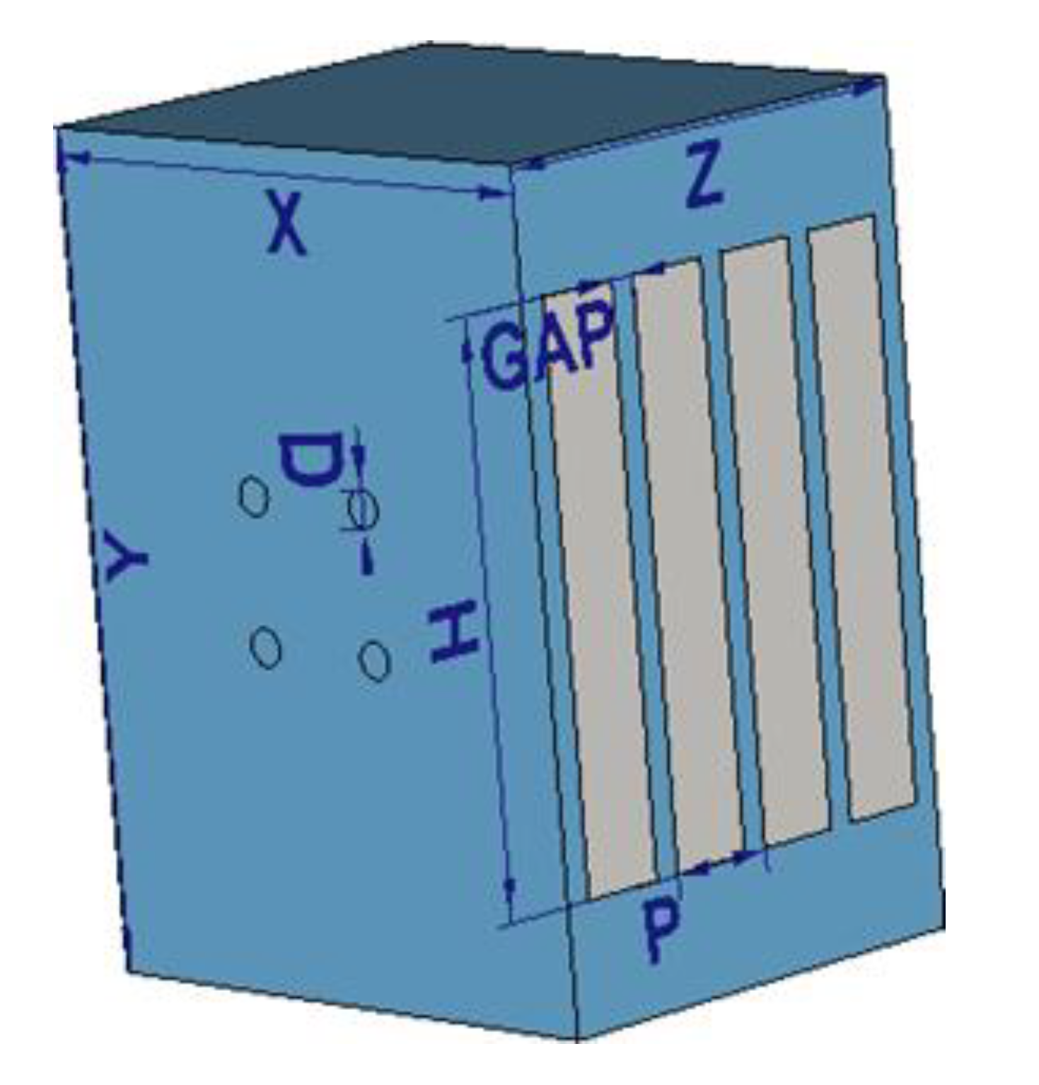
The intermediate cavity has been designed with the initial dimensions from the analytical formulas provided in Section II. The dimensions of the cavity have been optimized using electromagnetic simulation tools (eigenmode solver) to achieve the cavity parameters (the operating frequency and mode of operation matching the specification) for the desired performance of the klystron. A schematic diagram showing the geometrical parameters of the cavity used for optimization is shown in Figure 2.
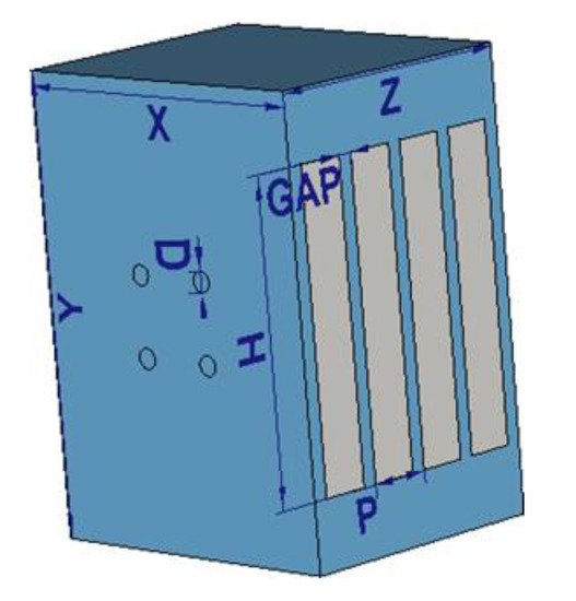
Figure 2.
RF cavity considered for simulation: ladder-type multibeam EIK intermediate cavity.
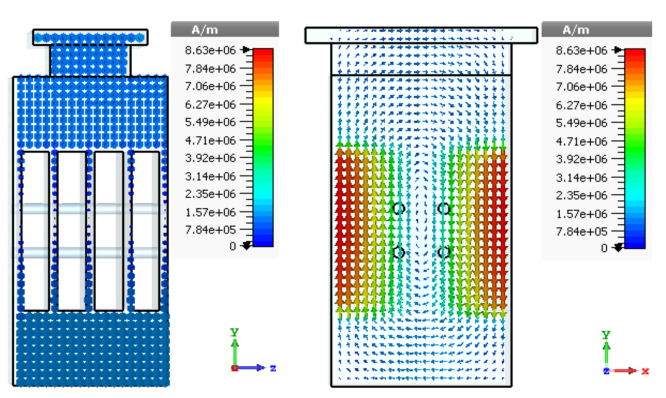
Figure 3 shows the cut-plane view of the electric field distribution of the operating mode inside the proposed intermediate cavity while Figure 4 shows the cut-plane view of the magnetic field pattern of the same. The frequency of the operating mode is found to be 28.53 GHz from the CST Microwave studio simulations, when taking the gap as 0.27 mm and the drift tube radius as 0.18 mm. Moreover, the shunt impedance of the operating mode is obtained to be 35.07 MΩ, Q = 720 and the R over Q is 48.7 according to the microwave studio calculations.
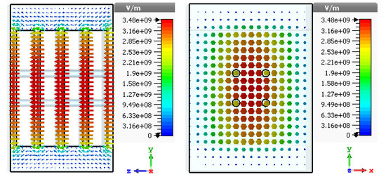
Figure 3.
Electric field distribution of the 2π mode (cut-plane view) for the intermediate cavities with CST.

Figure 4.
Magnetic field distribution of the 2π mode (cut-plane view) for the intermediate cavities with CST.
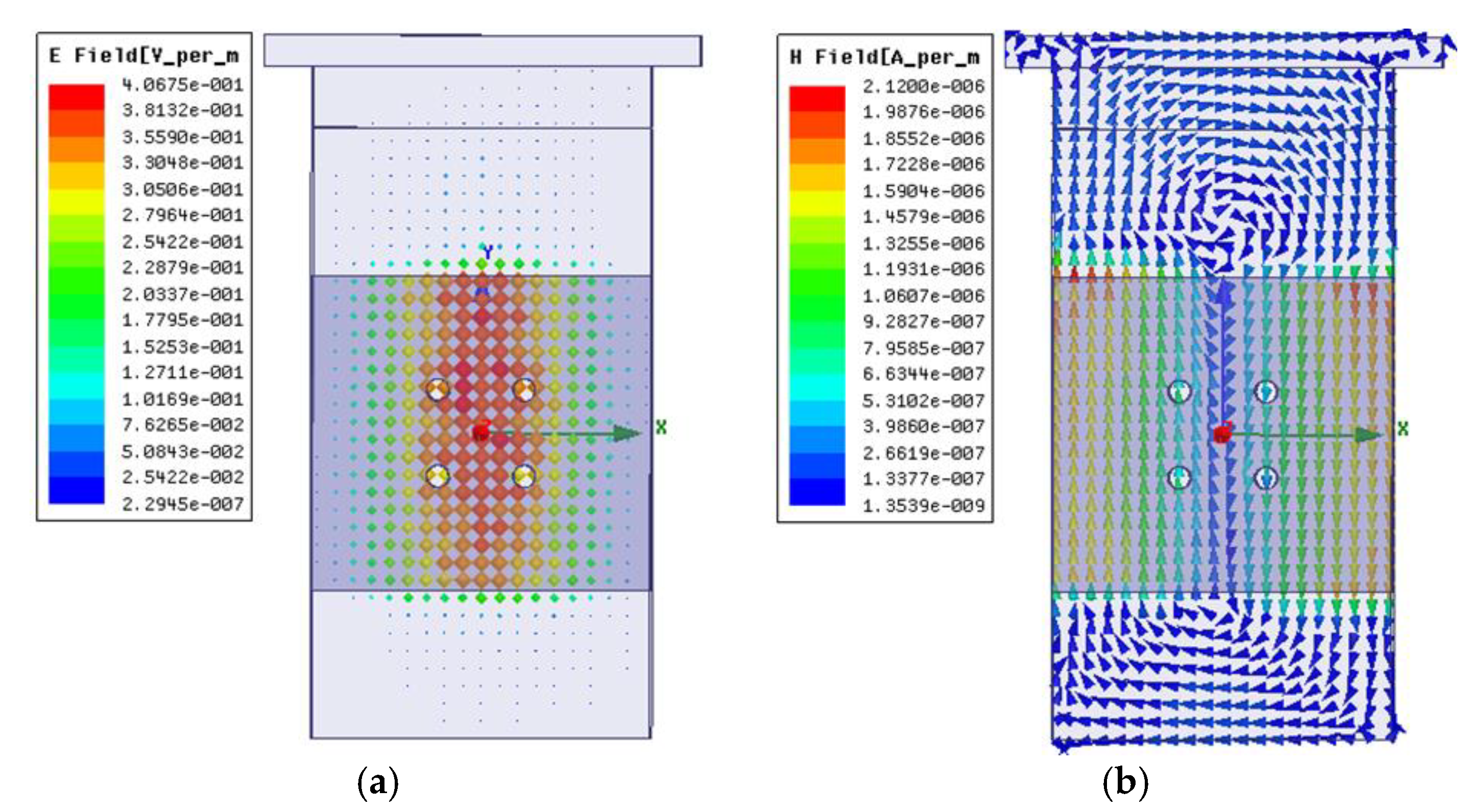
To validate the simulation results, the cavity has been simulated using ANSOFT HFSS. All the parameters, e.g., the resonant frequency, Q, and electric and magnetic field distribution of the operating mode of the proposed RF cavity, have been obtained from the HFSS simulation.
Figure 5a shows the electric field distribution of the cavity, and Figure 5b shows the magnetic field distribution of the proposed cavity. The frequency of the mode is found to be 28.52 GHz, and the quality factor is also found to be 708 from the HFSS simulations. The final optimized geometrical design parameters of the intermediate cavity for the Ka-band are given in Table 2, and the simulated results are shown in Table 3.
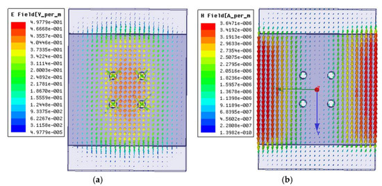
Figure 5.
Electric field and magnetic field distribution of the intermediate cavities with HFSS. (a) E-field distribution; (b) M-field distribution.
Table 2.
Optimized design parameters (intermediate cavity).
Table 3.
Comparison of the simulated cavity parameters (intermediate cavity).
3.2. Design of the Input/Output Cavities
The input and output cavities are the essential parts of the RF section of a klystron. In this section, the design and simulation of the input and output cavities have been discussed.
This step introduces a coupler in the output RF cavity to extract the power from the bunched electron beams. In addition, a coupler is introduced in the input RF cavity to introduce the RF signal for the modulation with the electron beams.
The designed input and output cavities with the slot coupling and attaching the WR28 waveguide for the standard Ka-band are shown in Figure 6. The optimized geometrical design parameters of the input/output cavities for the Ka-band are given in Table 4, and the simulated results are presented in Table 5.
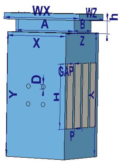
Figure 6.
RF cavity considered for simulation: ladder-type multibeam EIK input/output cavities.
Table 4.
Optimized design parameters (input/ output cavities).
Table 5.
Comparison of the simulated cavity parameters (input/ output cavities).
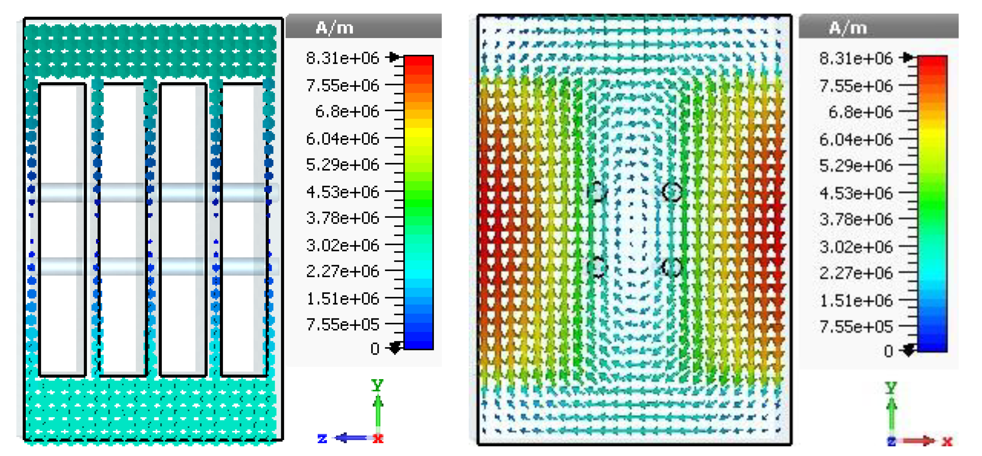
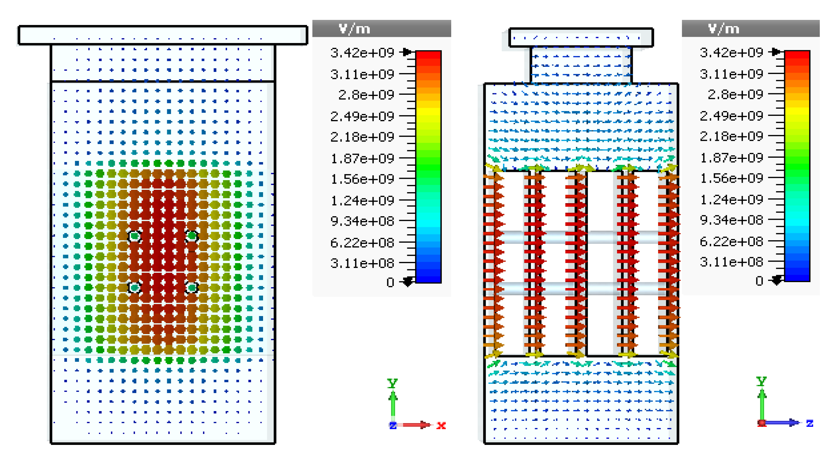
Figure 7 shows the cutting plane view of the electric field distribution of the proposed input and output cavities while Figure 8 shows a cutting plane view of the magnetic field pattern of the proposed input and output cavities. The mode frequency is found to be 28.53 GHz from the CST simulations, considering the gap and drift tube radius to be the same as those of the intermediate cavities. The quality factor of the cavities has been obtained as 720, and the calculated shunt impedance of the operating mode across the gaps is 31.85 MΩ. According to the CST calculations, the R over Q is estimated to be 44.2.
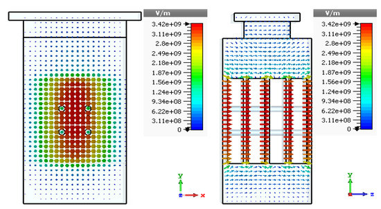
Figure 7.
Electric field distribution of the 2π mode (cut-plane view) for the input and output cavities with CST.

Figure 8.
Magnetic field distribution of the 2π mode (cut-plane view) for the input and output cavities with CST.
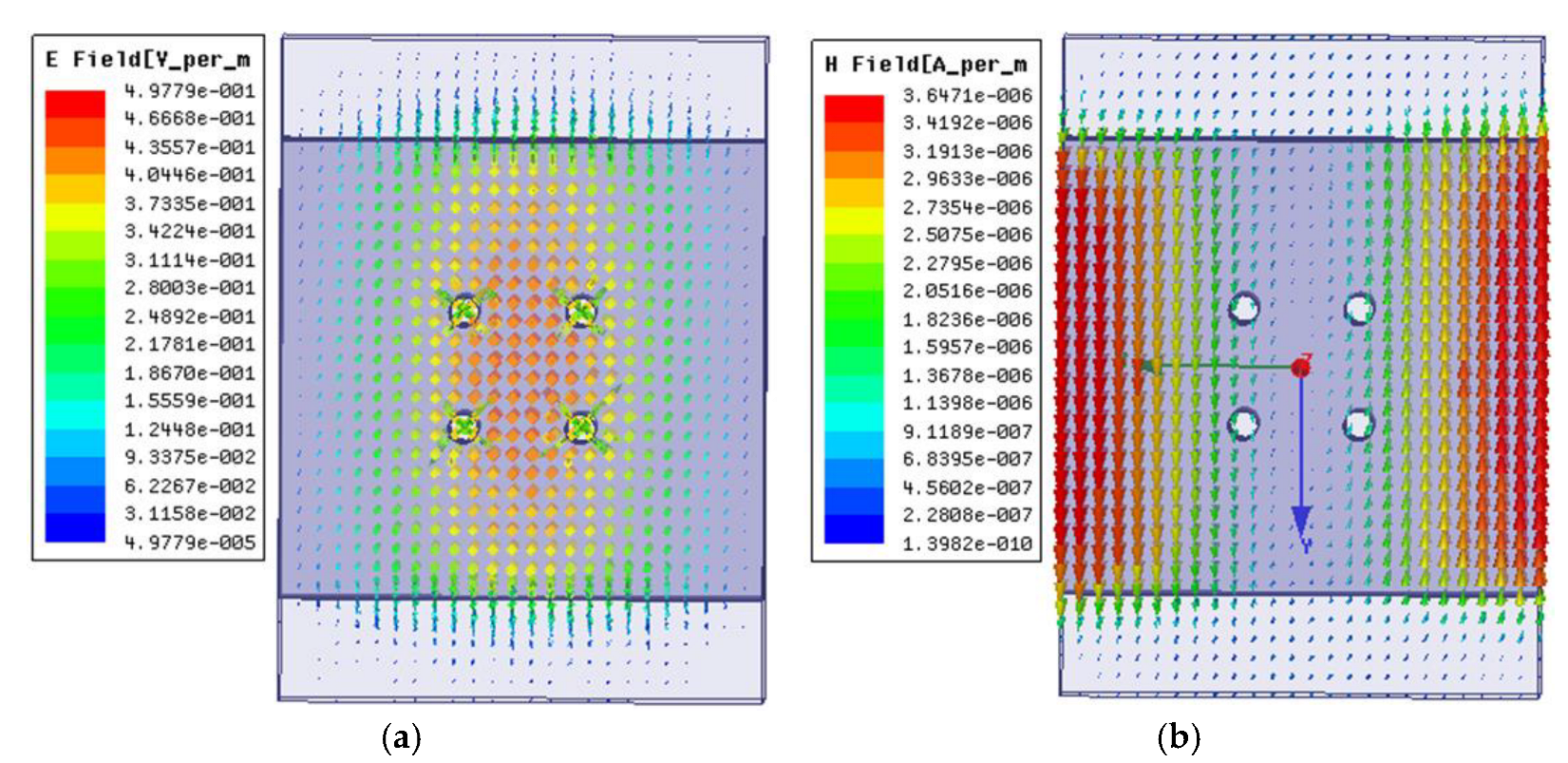
For the validation of the results, the same simulation has been performed using ANSOFT HFSS, considering the exact geometrical cavity dimensions considered for the CST simulation. Figure 9a,b show the electric and magnetic field distribution of the cavity. The operating-mode frequency and quality factor are 28.52 GHz and 702, respectively. The input and output cavities have an external Q factor (Qe) of about 38, dictated by the coupling of the cavity with the waveguide.
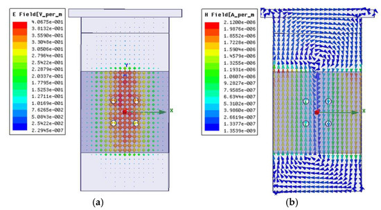
Figure 9.
Electric field distribution and magnetic field distribution of the input and output cavities with HFSS; (a) E-field distribution; (b) M-field distribution.
During the computation of the Q factor (using the eigenmode computation) of the operating mode, the standard material properties of copper (with an electrical conductivity of 5.96 × 10⁷ S/m) were considered. Because there are several metallic walls inserted within the cavity (the walls of the ladder structure), the wall losses are higher in the case of these cavities compared to the Ka-band cavities with a conventional structure. Therefore, the Q factor is lower compared to the conventional Ka-band cavities.
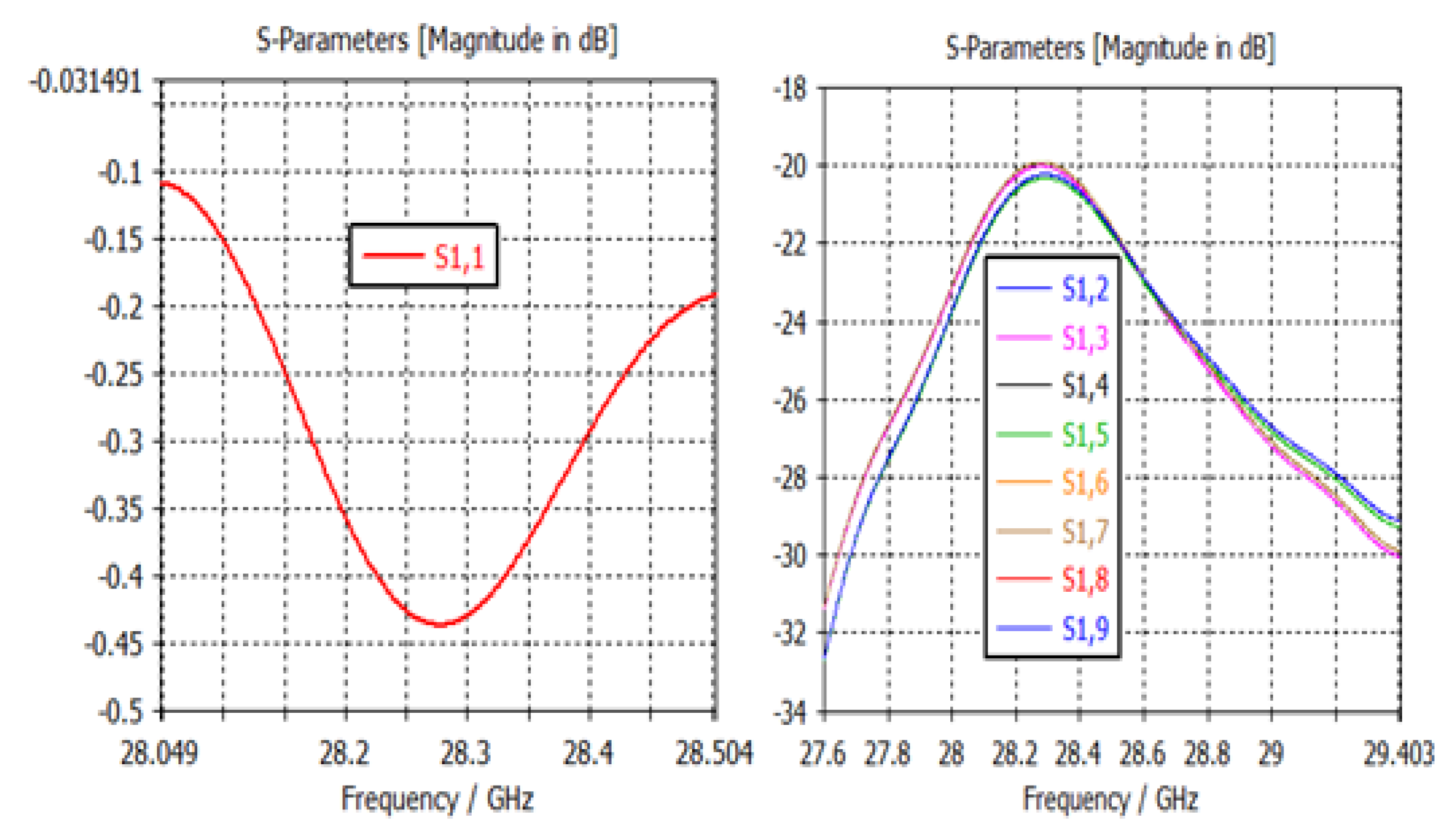
Figure 10 shows the geometry used for the time-domain simulation of the input and output cavities. In this step, a rectangular port (port 1) on the output waveguide coupler and a set of discrete ports (port 2 to 9) at the gap centers of different beamlets have been considered, as shown in Figure 10. The time-domain simulation has been carried out using a CST studio time-domain solver, and the obtained reflection and transmission coefficients are shown in Figure 11. The almost identical transmission parameters in Figure 11 clearly show a symmetric field distribution among the four beamlets’ gaps. The reflection parameter dip suggests a significant coupling of the electromagnetic energy through the coupling slot at the operating frequency.
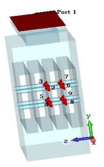
Figure 10.
RF cavity considered for simulation: ladder-type multibeam EIK input/output cavities with port.
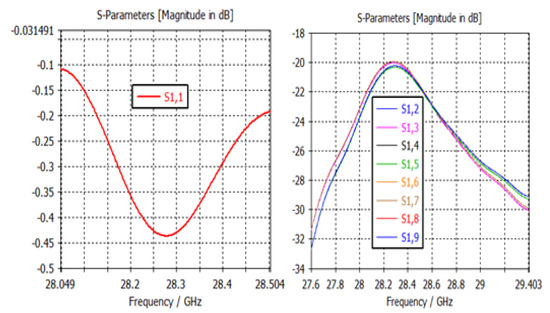
Figure 11.
S-parameters obtained from the time-domain simulation.
3.3. Design of the RF Section
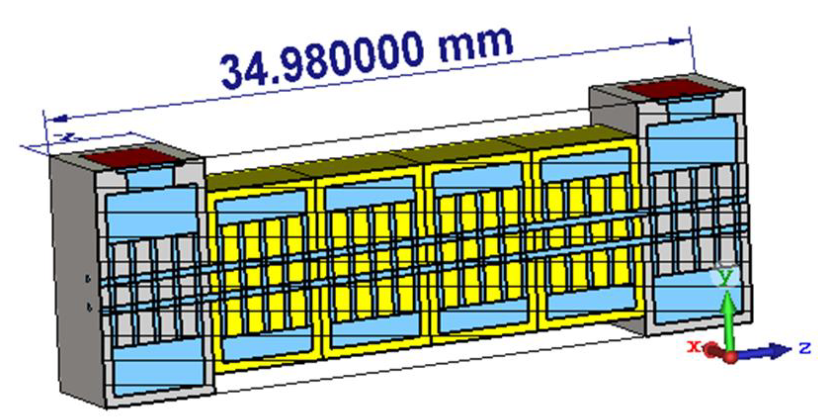
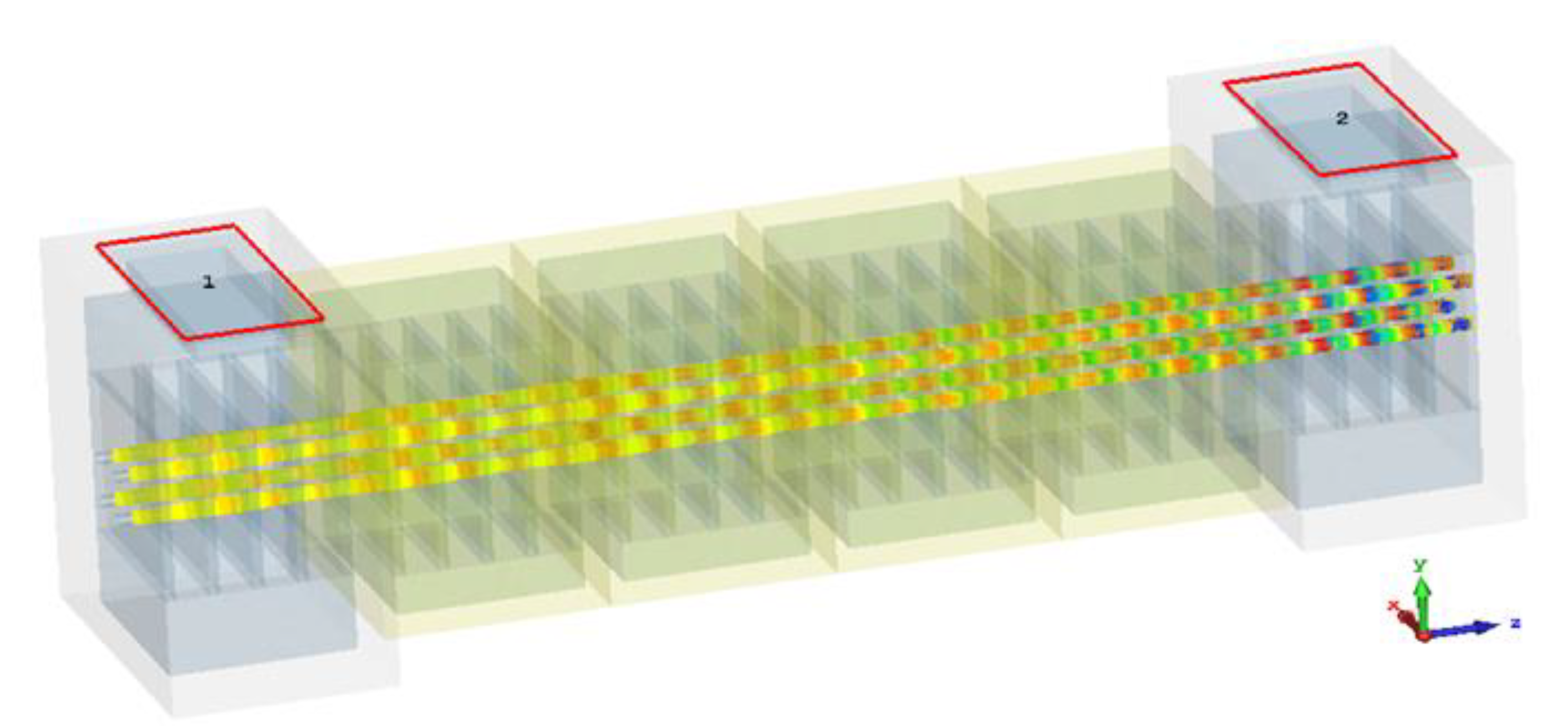
Figure 12 shows the cut-plane view of the RF section of the proposed four-beams EIK. The simulation geometry has been modeled and simulated using the CST PIC simulation tool. In this structure, six cavities (including the input and output cavities) have been considered. In this model, the center-to-center distance between the cavities has been taken as 5.83 mm and the length of the beam tunnel has been taken as 34.98 mm. The input signal used is a single-frequency sinusoidal signal with a constant amplitude. An axial magnetic field of 0.33 T (calculated according to Equation (15)) has been applied to maintain the focusing of the electron beam throughout the RF section. The frequency of the input signal has been swept in the complete frequency band of operation (i.e., 27.95 GHz to 28.95 GHz) to obtain the steady-state gain of the device. It may be noted that for each frequency point, the PIC simulation takes about 40 h to attain the steady state. A snapshot of the beam trajectory representing the bunching of the electrons at the output cavity and the phase space plot at 32 ns are shown in Figure 13 and Figure 14. The details of the input signal for one particular frequency point are shown in Figure 15 and Figure 16.
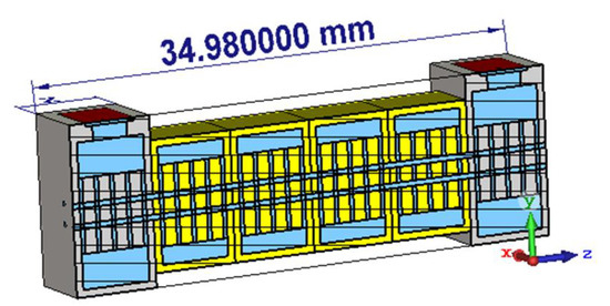
Figure 12.
Cut-plane of RF section of Ka-band ladder-type multibeam EIK.

Figure 13.
Beam–wave interaction of Ka-band ladder-type multibeam EIK.
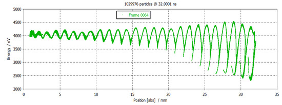
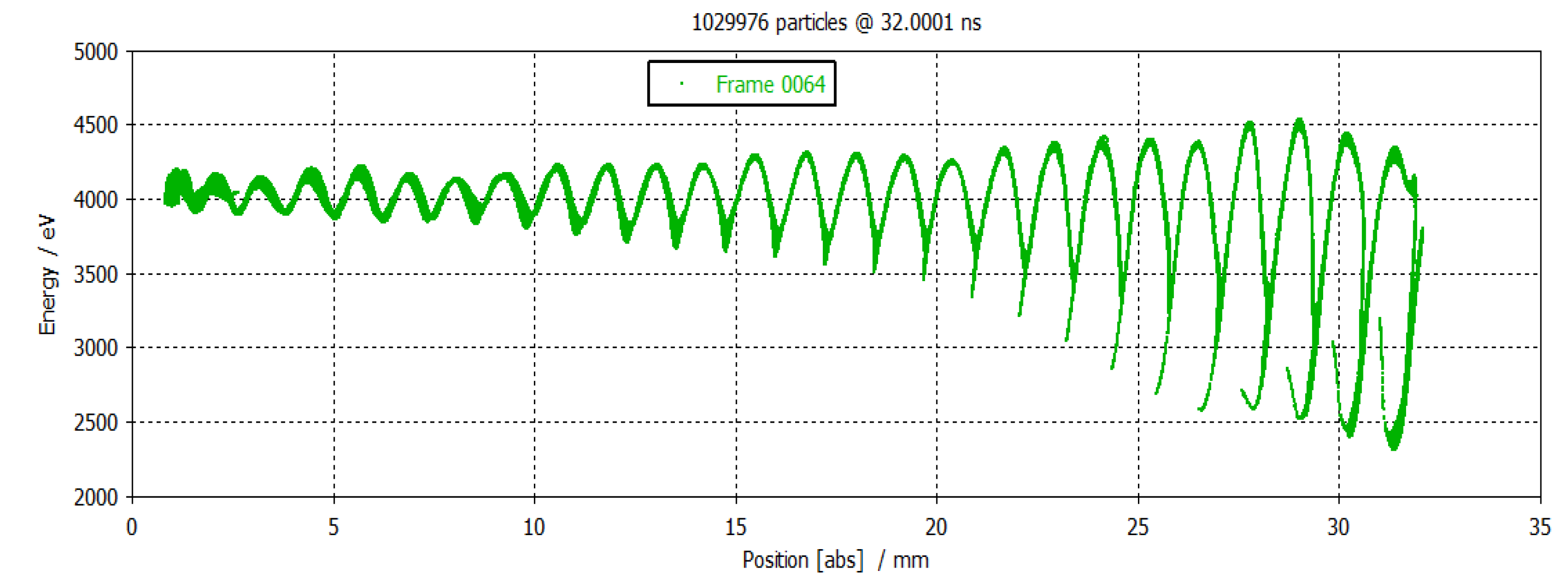
Figure 14.
Phase space plot of the particles at steady state (32 ns).
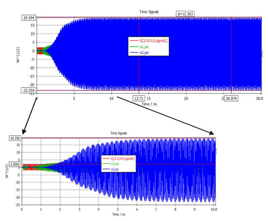
Figure 15.
Port signals (combined view) of RF section.
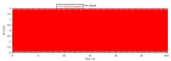
Figure 16.
Input port signal of RF section.
A snapshot of the electron beam trajectory of the PIC simulation is shown in Figure 12. The velocity modulation of the electron beam, which is the main indication of the RF amplification, is clearly visible at the output cavity of the device. Figure 14 shows the combined view of the input and output signals from the RF section. The signals have been recorded after the beam–wave interactions in the RF section.
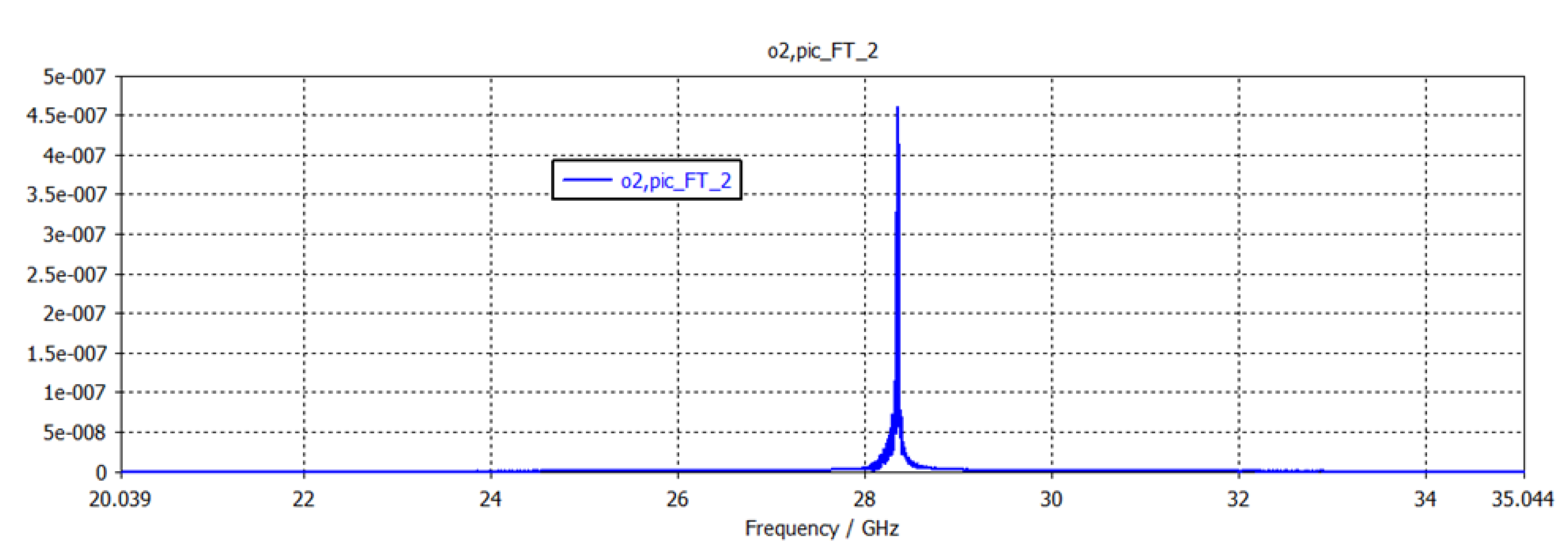
Figure 15 shows the input RF signal. This signal has been applied at the input port of the RF section. Figure 14 shows the output signal from the RF section. The output signal has been recorded at the output waveguide port after the beam–wave interactions in the RF section. From Figure 14, it can be observed that the maximum amplitude of the output signal is 19.39 √(watt), corresponding to an input signal of 2.0 √(watt) (peak). The peak output power calculated from the output signal is more than 375.97 W and the RMS output power is 187.98 W. The frequency spectrum of the output signal is shown in Figure 17. Figure 17 clearly shows the peak of the spectrum at 28.5 GHz.

Figure 17.
Frequency spectrum of the output signal.
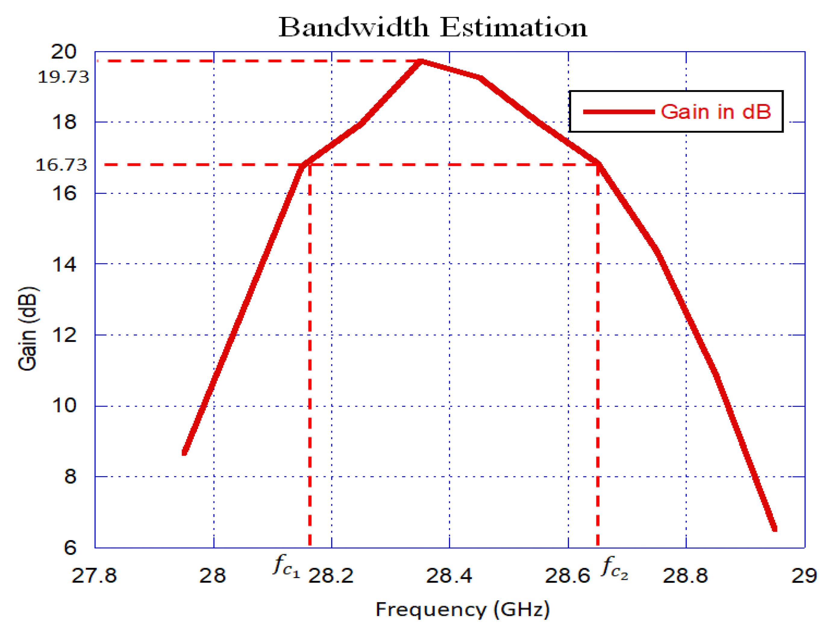
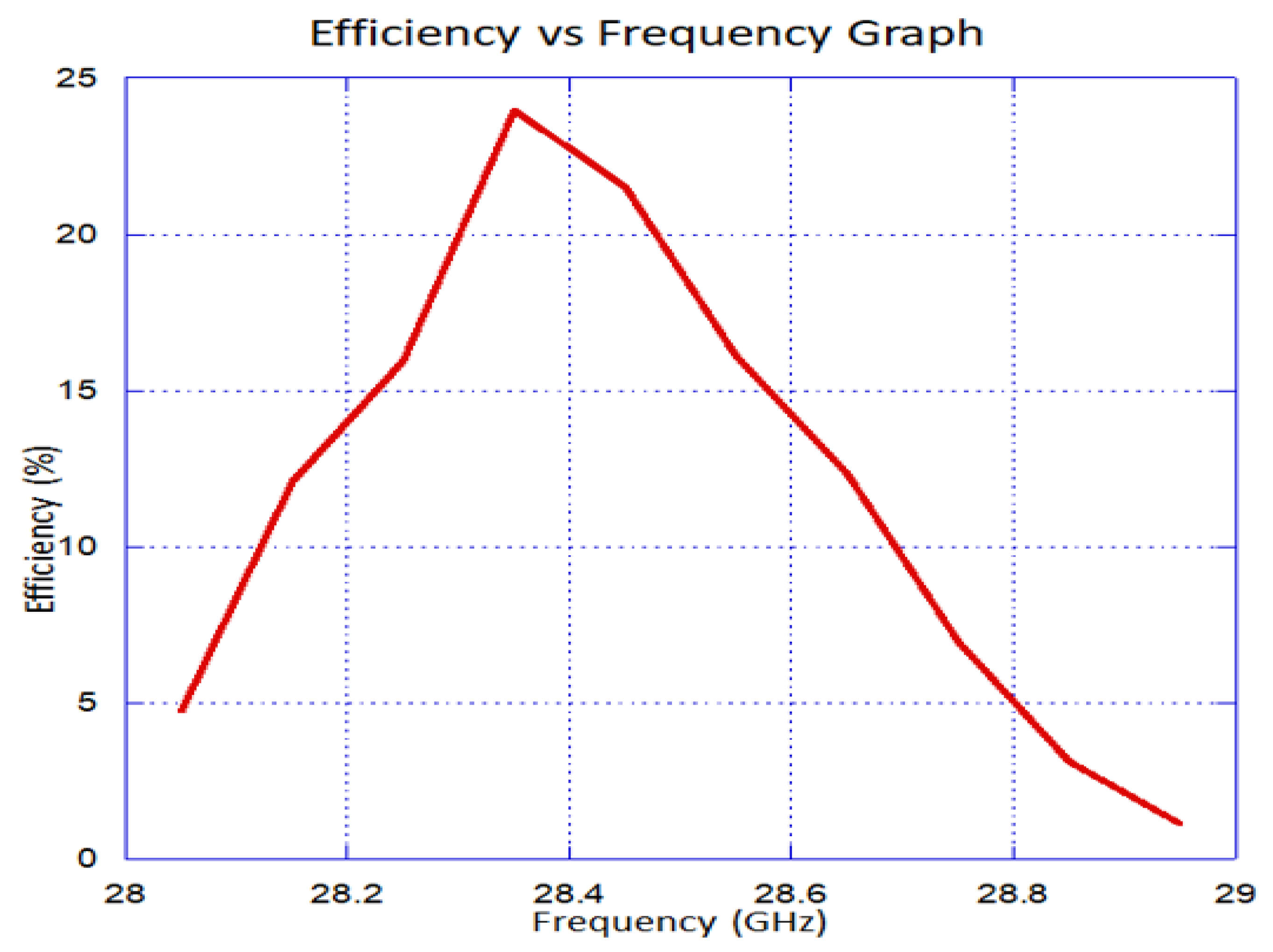
The gain of the RF section for different frequencies has been plotted in Figure 18, and the efficiency of the device in different frequencies is plotted in Figure 19. From this plot, the higher (fh) and lower (fl) −3 dB frequency points are found to be fh = 28.66 GHz and fl = 28.15 GHz. Therefore, the −3 dB bandwidth of the device can be calculated as 510 MHz. Similarly, the −1 dB bandwidth of the device comes out to be 180 MHz. The operating bandwidth of the device can be further increased by employing the stagger tuning of the intermediate cavities, i.e., tuning each individual cavity at slightly different frequencies.
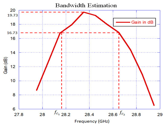
Figure 18.
Graphical representation of gain vs. frequency.
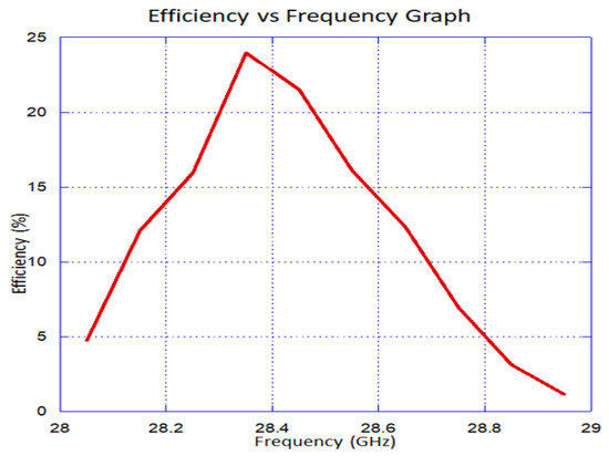
Figure 19.
Graphical representation of efficiency vs. frequency.
The simulation results of the RF section have been provided in Table 6. The slight variation in the gain in the operating band (28.15 GHz to 28.66 GHz) can be managed by gain-equalizing schemes, where the input signal amplitude and beam voltages are adjusted to achieve a flatness of the gain at desired frequency band/sub-bands. This scheme is widely used in travelling wave tube (TWT)-based communication systems, especially in satellite communication.
Table 6.
Results of proposed multiple beam klystron.
The fabrication of the RF section (with a 34.98 mm total length, gap length of 0.27 mm, ladder wall height of 5.5 mm, and cavity height of 7.96 mm) can be conducted using the wire-cut Electric Discharge Machining (EDM) technique, where the upper and lower walls (top and bottom) of the cavity may be fabricated separately. This fabrication possibility is currently being explored through advanced precision tool room centers because we do not have in-house precision fabrication facilities.
4. Conclusions
The design of the RF section of a ladder-shaped multibeam extended interaction klystron operating at 4 kV has been presented. The ladder-type intermediate and input/output resonant cavities operating at the Ka-band are compatible with 3D printing or microfabrication techniques. The RF section has been designed and analyzed using the commercially available 3D electromagnetic simulation software. The dimensions of the RF cavity have been optimized, and the dimensions of the RF cavity have been optimized for getting different cavity parameters, such as the resonant frequency and the R over Q. The 3D PIC code simulation results of the proposed RF section have been reported with the estimation of the bandwidth, output power, and gain. The bandwidth of the device is found to be 510 MHz with a stable output power of 375.97 W. These devices can be utilized in high-data-rate wireless communications, such as airborne RADAR, 5G communication, etc.
Author Contributions
All authors contributed to the conceptualization, methodology, analyses, and review and editing. The design and validation were done by S.M. The formal analysis was done by S.M. and M.S.K. S.M. and A.K.B. prepared the draft manuscript. S.M. worked under the guidance of C.K., D.P. and A.K.B. All authors have read and agreed to the published version of the manuscript.
Funding
This research was funded by IIT Guwahati Technology Innovation and Development Foundation sponsored by the Department of Science and Technology (DST) grant number [TIH/TD/0303] and The APC was funded by [TIH/TD/0303].
Acknowledgments
The authors would like to thank the IIT Guwahati Technology Innovation and Development Foundation sponsored by the Department of Science and Technology (DST) for providing financial assistance to carry out the research work.
Conflicts of Interest
The authors declare no conflict of interest.
References
- Liao, S.Y. Microwave Devices and Circuits, 3rd ed.; Pearson Education: Noida, India, 2003; ISBN 9788177583533/8177583530. [Google Scholar]
- Gilmour, A.S., Jr. Microwave Tubes; ArtechHouse: Nordwood, MA, USA, 1986. [Google Scholar]
- Smith, M.J.; Phillips, G. Power Klystrons Today. Research Studies Press Ltd.: Baldock, UK, 1995. [Google Scholar]
- Korolyov, A.N.; Gelvich, E.A.; Zhary, Y.V.; Zakurdayev, A.D.; Poognin, V.I. Multiple-beam Klystron Amplifiers: Performance Parameters and Development Trends. IEEE Trans. Plasma Sci. 2004, 32, 1109–1117. [Google Scholar] [CrossRef]
- Nguyen, K.T.; Abe, D.K.; Pershing, D.E.; Levush, B.; Wright, E.L.; Bohlen, H.; Staprans, A.; Zitelli, L.; Smithe, D.; Pasour, J.A.; et al. High-power Four Cavity S-band Multiple-beam Klystron Design. IEEE Trans. Plasma Sci. 2004, 32, 1119–1135. [Google Scholar] [CrossRef]
- Maity, S.; Bandyopadhyay, A.K.; Joshi, L.M. Design of Radio Frequency Cavities for a J-Band Multibeam Klystron. IETE J. Res. 2012, 58, 310–316. [Google Scholar] [CrossRef]
- Larionov, A.; Teryaev, V.; Matsumoto, S.; Chin, Y.H. Design of multi-beam klystron in X-band. Proceeding of the 27th Linear Accelerator Meeting in Japan, Kyoto, Japan, 7–9 August 2002. [Google Scholar]
- Bandyopadhyay, A.K.; Maity, S.; Joshi, L.M.; Kant, D.; Singh, A.K. Design of the Radio Frequency Section of a Multiple Beam Klystron working in the J-band Frequency Range. In Proceedings of the IEEE 14th International Vacuum Electronics Conference (IVEC), Paris, France, 21–23 May 2013. [Google Scholar] [CrossRef]
- Bandyopadhyay, A.K.; Joshi, L.M.; Pal, D.; Kant, D.; Meena, R.; Kumar, B.; Maity, S.; Rawat, V.S.; Saha, S. Development of the Radiofrequency Section of a Ku-band Multiple-Beam Klystron. IETE J. Res. 2016, 62, 859–865. [Google Scholar] [CrossRef]
- Shin, Y.M.; Park, G.S.; Scheitrum, G.P.; Caryotakis, G. Circuit Analysis of an Extended Interaction Klystron. J. Korean Phys. Soc. 2004, 44, 1239–1245. [Google Scholar]
- Li, R.; Ruan, C.; Zhang, H.; He, Y.; Shan, S. Improvement of Output Power in G-band EIK with Optimized and Tapering Gap Length. In Proceedings of the IEEE International Vacuum Electronics Conference (IVEC), Monterey, CA, USA, 24–26 April 2018; pp. 24–26. [Google Scholar] [CrossRef]
- Chang, Z.; Meng, L.; Yin, Y.; Wang, B.; Li, H.; Rauf, A.; Ullah, S.; Bi, L.; Peng, R. Circuit Design of a Compact 5-kV W-Band Extended Interaction Klystron. IEEE Trans. Electron Devices 2018, 65, 1179–1184. [Google Scholar] [CrossRef]
- Roitman, A.; Berry, D.; Steer, B. State-of-the-art W-band extended interaction klystron for the CloudSat program. IEEE Trans. Electron Devices 2005, 52, 895–898. [Google Scholar] [CrossRef]
- Nguyen, K.T.; Pershing, D.; Wright, E.L.; Pasour, J.; Calame, J.; Ludeking, L.; Rodgers, J.; Petillo, J. Sheet-beam 90 GHz and 220 GHz extendinteraction-klystron designs. In Proceedings of the IEEE IVEC, Kitakyushu, Japan, 15–17 May 2007; pp. 1–2. [Google Scholar] [CrossRef]
- Durand, A.J.; Durand, A.J. PPM focused Ku band pulsed EIK. In Proceedings of the IEEE International Vacuum Electronics Conference held Jointly with 2006 IEEE International Vacuum Electron Sources, Monterey, CA, USA, 25–27 April 2006; pp. 73–74. [Google Scholar] [CrossRef]
- Berry, D.; Deng, H.; Dobbs, R.; Horoyski, P.; Hyttinen, M.; Kingsmill, A.; Machattie, R.; Sokol, E.; Steer, B. Practical aspects of EIK technology. IEEE Trans. Electron Devices 2014, 61, 1830–1835. [Google Scholar] [CrossRef]
- Wright, E.L.; Shabazian, A.; Cecil, M. Ka-band klystron amplifiers for satellite communications and scientific applications. Abstracts. In Proceedings of the International Vacuum Electronics Conference 2000 (Cat. No.00EX392), Monterey, CA, USA, 2–4 May 2000; p. 2. [Google Scholar] [CrossRef]
- Behtouei, M.; Faillace, L.; Ferrario, M.; Spataro, B.; Variola, A. Initial Design of a High-Power Ka-Band Klystron. J. Phys. Conf. Ser. 2020, 1596, 012023. [Google Scholar] [CrossRef]
- Cai, J.C.; Syratchev, I.; Burt, G. Design Study of a High-Power Ka-Band High-Order-Mode Multibeam Klystron. IEEE Trans. Electron Devices 2020, 67, 5736–5742. [Google Scholar] [CrossRef]
- Chodorow, M.; Kulke, B. An extended-interaction klystron: Efficiency and bandwidth. IEEE Trans. Electron Devices 1966, ED-13, 439–447. [Google Scholar] [CrossRef]
- Barker, R.J.; Booske, J.H.; Luhmann, N.C.; Nusinovich, G.S. Klystrons in Modern Microwave and Millimeter-Wave Power Electronics, 1st ed.; IEEE Press: Piscataway, NJ, USA, 2005; pp. 131–147. [Google Scholar]
- Campbell, C.F.; Nayak, S.; Kao, M.; Chen, S. Design and performance of 16–40GHz GaN distributed power amplifier MMICs utilizing an advanced 0.15µm GaN process. In Proceedings of the 2016 IEEE MTT-S International Microwave Symposium (IMS), San Francisco, CA, USA, 22–27 May 2016; pp. 1–4. [Google Scholar] [CrossRef]
- Neininger, P.; John, L.; Zink, M.; Meder, D.; Kuri, M.; Tessmann, A.; Friesicke, C.; Mikulla, M.; Quay, R.; Zwick, T. Broadband 100-W Ka-Band SSPA Based on GaN Power Amplifiers. IEEE Microw. Wirel. Compon. Lett. 2022, 32, 708–711. [Google Scholar] [CrossRef]
- Bi, L.; Meng, L.; Yin, Y.; Xu, C.; Zhu, S.; Peng, R.; Zeng, F.; Chang, Z.; Wang, B.; Li, H.; et al. Design and Analysis of a High-Order Mode Ladder-Type RF Circuit for Stable Operation in a W-Band Extended Interaction Oscillator. IEEE Trans. Electron Devices 2019, 66, 729–735. [Google Scholar] [CrossRef]
- Li, S.; Ruan, C.; Fahad, A.K.; Wang, P.; Zhang, Z.; He, W. Novel Coupling Cavities for Improving the Performance of G-Band Ladder-Type Multigap Extended Interaction Klystrons. IEEE Trans. Plasma Sci. 2020, 48, 1350–1356. [Google Scholar] [CrossRef]
- Zhao, D.; Liu, G.; Gu, W.; Ma, T.; Xue, Q.; Zhang, Z. Development of a High Power Ka-Band Extended Interaction Klystron. In Proceedings of the IEEE International Vacuum Electronics Conference (IVEC), Busan, Korea, 28 April–1 May 2019. [Google Scholar]
- Li, R.; Ruan, C.; Zhang, H. Design and optimization of G-band extended interaction klystron with high output power. Phys. Plasmas 2018, 25, 033107. [Google Scholar] [CrossRef]
- Lv, S.; Zhang, C.; Wang, S.; Wang, Y. Stability analysis of a planar multiple-beam circuit forW-band high-power extended-interaction klystron. IEEE Trans. Electron Devices 2015, 62, 3042–3048. [Google Scholar] [CrossRef]
- Yin, Y.; Zeng, F.; Wang, B.; Li, H.; Bi, L.; Chang, Z.; Peng, R.; Zhu, S.; Xu, C.; Meng, L.; et al. Preliminary Study of a Multiple-Beam Extended-Interaction Oscillator with Coaxial Structure. IEEE Trans. Electron Devices 2018, 65, 2108–2113. [Google Scholar] [CrossRef]
- Qin, Y.; Yin, Y.; Xu, C.; Yang, T.; Chen, Q.; Xu, X.; Xie, J.; Bi, L.; Wang, B.; Li, H.; et al. Analysis of the Resonator Part of a Ka-Band Multiple-Beam Extended-Interaction Oscillator through Electric Field Uniformity. Electronics 2021, 10, 276. [Google Scholar] [CrossRef]
- Lin, F.-M.; Wu, S.; Xiao, Y.; Zhang, L. A 0.3 THz Multi-Beam Extended Interaction Klystron Based on TM10,1,0 Mode Coaxial Coupled Cavity. IEEE Access 2020, 8, 214383–214391. [Google Scholar] [CrossRef]
- Maity, S.; Kumar, M.; Koley, C.; Pal, D.; Bandyopadhyay, A. Design and Simulation of Extended Interaction Cavities for a Ka band Multi beam Klystron. DSJ 2021, 71, 320–323. [Google Scholar] [CrossRef]
- Zhang, X.; Zhang, R.; Wang, Y.; Chao, Q.; Xie, B.; Chen, H.; Guo, N. Design study of a W-band high power extended interaction klystron based on the coaxial high-order mode. AIP Adv. 2021, 11, 125210. [Google Scholar] [CrossRef]
- Wang, D.; Wang, G.; Wang, J.; Li, S.; Zeng, P.; Teng, Y. A high-order mode extended interaction klystron at 0.34 THz. Phys. Plasmas 2017, 24, 023106-1–023106-8. [Google Scholar] [CrossRef]
- Wright, E.; Balkcum, A.; Bohlen, H.; Cattelino, M.; Cox, L.; Cusick, M.; Falce, L.; Friedlander, F.; Stockwell, B.; Zitelli, L. Development of a 10-MW, L-band, multiple-beam klystron for TESLA. In Proceedings of the IEEE Particle Accelerator Conference, Portland, OR, USA, 12–16 May 2003. [Google Scholar] [CrossRef]
- Zhang, X.; Zhang, R.; Wang, Y. Research on a High-Order Mode Multibeam Extended-Interaction Oscillator with Coaxial Structure. IEEE Trans. Plasma Sci. 2020, 48, 1902–1909. [Google Scholar] [CrossRef]
- Chodorow, M.; Wessel-Berg, T. A high-efficiency klystron with distributed interaction. IRE Trans. Electron Devices 1961, 8, 44–55. [Google Scholar] [CrossRef]
- Symons, R.S.; Vaughan, R.M. The linear theory of the clusteredcavity klystron. IEEE Trans. Plasma Sci. 1994, 22, 713–718. [Google Scholar] [CrossRef]
- User’s Manual, CST Studio Suite—2019; Dassault Systems: Vélizy-Villacoublay, France, 2019.
- Ansoft HFSS (Version 10), Users Manual, Ansoft Corporation. Available online: http://www.ansys.com (accessed on 22 September 2012).


Publisher’s Note: MDPI stays neutral with regard to jurisdictional claims in published maps and institutional affiliations. |
© 2022 by the authors. Licensee MDPI, Basel, Switzerland. This article is an open access article distributed under the terms and conditions of the Creative Commons Attribution (CC BY) license (https://creativecommons.org/licenses/by/4.0/).