1. Introduction
Nowadays, sensing devices find applications in almost every industrial area spanning from automotive to agriculture and from healthcare to avionic. The wide diffusion of these devices is due to their capacity to convert physical and chemical parameters into electric signals that can be transmitted and elaborated. For healthcare applications, biomedical sensors are used to measure in situ human body parameters and must be dressed or even implanted in patients often affected by important diseases. Some diseases, in fact, require the dressing or the implanting of sensors for the continuous monitoring of specific medical parameters, such as the glucose level in the blood, that may, as a result, be uncomfortable for the patients. In this sense, biomedical sensors and their front-end interfaces are the key elements for the implementation of personalized telemedical diagnostic and therapeutic [
1,
2]. In general, sensors for clinical recordings use electrodes that, for certain diseases, must be worn even for long-term periods. For this reason, the electrodes need to be comfortable and guarantee high compatibility with organic tissues.
Among the various suitable electrodes, the optical ones (i.e., the optrodes) find applications in photoplethysmography (PPG) [
3,
4,
5], transcutaneous blood gas monitoring [
6], and neural interfaces [
7,
8] by using different optical techniques such as light absorption, fluorescence, and refractometry. In particular, PPG is a non-invasive optical measurement used to detect blood volume changes in vascular tissue and comprises a wide range of medical applications, such as measuring oxygen saturation, blood pressure, and cardiac signals. In general, for biomedical applications, the development of optical sensing devices requires low-cost and portable technology operating in low-voltage, low-power conditions. These requirements can be fulfilled by employing integrated optoelectronics sensors in standard CMOS technology combined with digital-based pulse-wave analysis techniques [
9,
10]. Optical sensor systems are also widely used in other fields of safety-healthcare applications, such as in wearable prosthetic systems [
11,
12,
13,
14], where a single or array of sensors are designed to increase the day-to-day patient life quality. Another important application of wearable optical sensors is the continuous environmental monitoring of workplaces where hazardous gases or nano- and/or micro-sized pollutants are employed with the aim of guaranteeing the health and safety of persons there operating [
15,
16,
17].
Each one of the above-mentioned applications requires the detection of chemical and biochemical substances as well as biological parameters guaranteeing high resolution, high sensitivity, and accuracy of the measurements. In general, optical sensors are devices composed of a semiconductor laser or which are LED emitting at the wavelength required from the specific application and of the Si photodiode (PD) that generates a photocurrent proportional to the light intensity illuminating its sensitive area. The electronic analog front-end of optical sensors is typically based on transimpedance amplifiers (TIA) that convert the input photocurrent to an amplified voltage signal operating, as much as possible, under low-voltage and low-power conditions [
9,
18,
19,
20,
21]. Moreover, in several applications, the TIA should provide a high gain and be supported by a real-time automatic gain control/compensation sub-system. In this sense, fine and coarse gain tunability should also be included and suitably implemented, while still guaranteeing a proper large bandwidth [
18,
19,
20]. In addition, especially referring to implantable solutions, the total required Si area should also be reduced as much as possible so as to achieve low-cost solutions as well [
22,
23,
24,
25,
26,
27,
28,
29].
The present paper reports on the design, fabrication, and characterization of a 180 nm CMOS fully integrated optoelectronic sensing system composed of a Si PD and a TIA acting as its electronic analog front-end for the conditioning of the photocurrent generated by the PD. The TIA circuit has been designed at the transistor level to manage nanoampere input photocurrents, operates at a 1.8 V single supply with a maximum power consumption of about 54 µW, and requires a Si area of 0.002 mm2. However, the designed TIA architecture makes the proposed solution suitable for any application where the sensing device generates a current proportional to the physical/chemical/biological parameter to be detected and measured. The integrated Si PD is based on a PNP junction and occupies a Si area of 0.01 mm2. The developed ASIC allows variable gains of up to 123 dBΩ to be achieved with a bandwidth of 500 kHz so that the result is suitable for optoelectronic sensing systems in biomedical applications.
The results of a series of experimental measurements are reported and discussed in detail for the electrical and optical characterization of the fabricated ASIC. Moreover, as a case example, it is demonstrated how the complete integrated system can be used as an optoelectronic sensing device for biomedical applications by optically detecting emulated standard electrocardiography (ECG) and PPG signal patterns.
2. ASIC Design and Fabrication
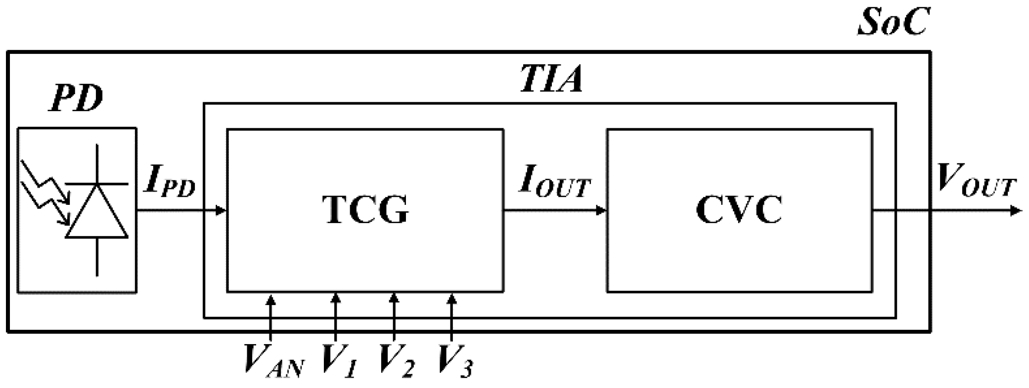
The overall block scheme illustrating the main stages of the proposed integrated optoelectronic sensing system on chip (SoC) is shown in
Figure 1. The photocurrent
IPD generated by the PD is the input signal of the tunable current gain (TCG) stage based on a current mirror architecture that amplifies the photocurrent signal with a specific gain which is settable by acting on the external voltages
V1,
V2, and
V3. These voltages are the digital control signals for the electronic circuit coarse gain tuning, while the additional external analog control voltage signal
VAN performs the fine gain tuning so as to provide the amplified output current
IOUT. This current, in turn, is the input signal of the subsequent current to voltage conversion (CVC) stage, based on a modified regulated cascode TIA (RGC-TIA) circuit topology [
22,
30,
31], and provides the output voltage signal
VOUT.
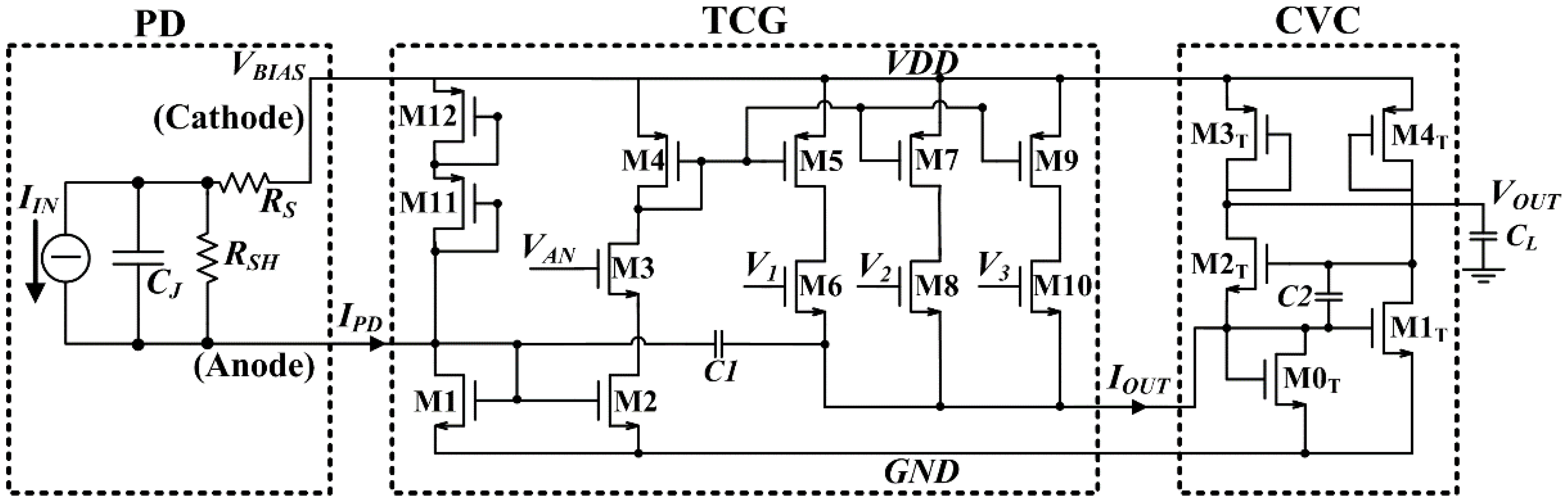
Figure 2 shows the schematic at the transistor level of the proposed TIA circuit designed in TSMC 180 nm CMOS technology. In this respect,
Table 1 reports: (i) the main parameters of all the employed transistors, the channel width (W) and length (L) expressed in µm, and the transconductance values under different operation conditions obtained by varying the external voltages; (ii) the values of the employed capacitors of
C1,
C2, and
CL; (iii) the shunt
RSH, the in-series
RS resistances, and the junction capacitance
Cj characterizing the integrated Si PD. The overall circuit, powered at a 1.8 V single supply voltage, has been developed in the CADENCE design system environment.
Referring to
Figure 2, the first stage of the architecture is the standard electrical model emulating a Si PD, operating in the photoconductive regime, that is composed of the following internal elements: an ideal current generator providing the photocurrent
IIN proportional to the light power impinging on the PD sensitive area, the junction capacitance
CJ, the shunt resistance
RSH, and the in-series resistance
RS. In addition, the PD cathode terminal is supplied through the voltage node
VBIAS connected directly to the overall power supply
VDD = 1.8 V. Thus, the PD anode provides the
IPD photocurrent signal at the input of the subsequent TCG stage that is based on a current mirror scheme capable to amplify the input current with a gain settable through the digital voltage signals
V1,
V2, and
V3 (individually activated). These external signals act on the gates of the transistors M6, M8, and M10, respectively, and select, in mutual exclusion, one of the three PMOS-based current mirror branches composed by the transistor pairs M4–M5, M4–M7, or M4–M9. The selected PMOS-based current mirror stage is preceded by an always active NMOS-based current mirror implemented by the transistor pair M1–M2. An additional external analog control voltage signal
VAN, acting on the gate of the transistor M3 that operates in the triode region as a voltage-controlled resistor, is also included to achieve a fine-tuning of the current gain and to allow for a proper amplified output current
IOUT and for compensations of the possible transistor mismatches. Moreover, the diode-connected transistors M11 and M12 implement the active loads of the basic current mirror architecture. The amplified current
IOUT provided by the TCG stage is the input signal of the CVC stage. As shown in
Figure 2, the input current flows in this stage through the diode-connected transistor M0
T. Moreover, the transistor M2
T, with its source connected to the input of this stage and considering M3
T as its active load, is properly regulated by a common source voltage amplifier implemented by the M1
T and M4
T transistors. Finally, the stability of the system is guaranteed by the two capacitors,
C1 and
C2, in feedback connections.
From the complete theoretical analysis, the transimpedance gain
ZTOT(f) of the electronic circuit as a function of the frequency is given by the following equation:
where
G(f) is the current gain of the TCG stage and
Z(f) is the transimpedance gain of the CVC stage. In particular, the analytical expression of
Z(f) is:
where
gm(.)’s are the transconductances referred to each specified transistor, and
j is the imaginary unit. Moreover,
CIN and
COUT are the total capacitances at the CVC stage input and output nodes, respectively. Referring to
Figure 2, these capacitances are equal to:
where
CPAR_IN is the parasitic capacitance at the input of the stage and
CPAR_OUT is the parasitic capacitance at the final output node of the system combined with the load capacitance
CL. The current gain
G(f) can be expressed as follows:
where the parameter
A depends on
VAN and represents the current mirror ratios achieved by neglecting the transistor parasitic capacitances and considering that the transistors M5, M7, and M9 are active one at a time as a function of the enabling signals
V1,
V2, and
V3. Under these conditions, the current mirror ratios related to each one of the transistors M5, M7, and M9 are equal to:
Moreover, in Equation (4),
Z1 is the input impedance of the TCG stage at the
IPD input node, and
Z2 is the input impedance of the CVC stage at the
IOUT input node. The values of these impedances can be calculated as follows:
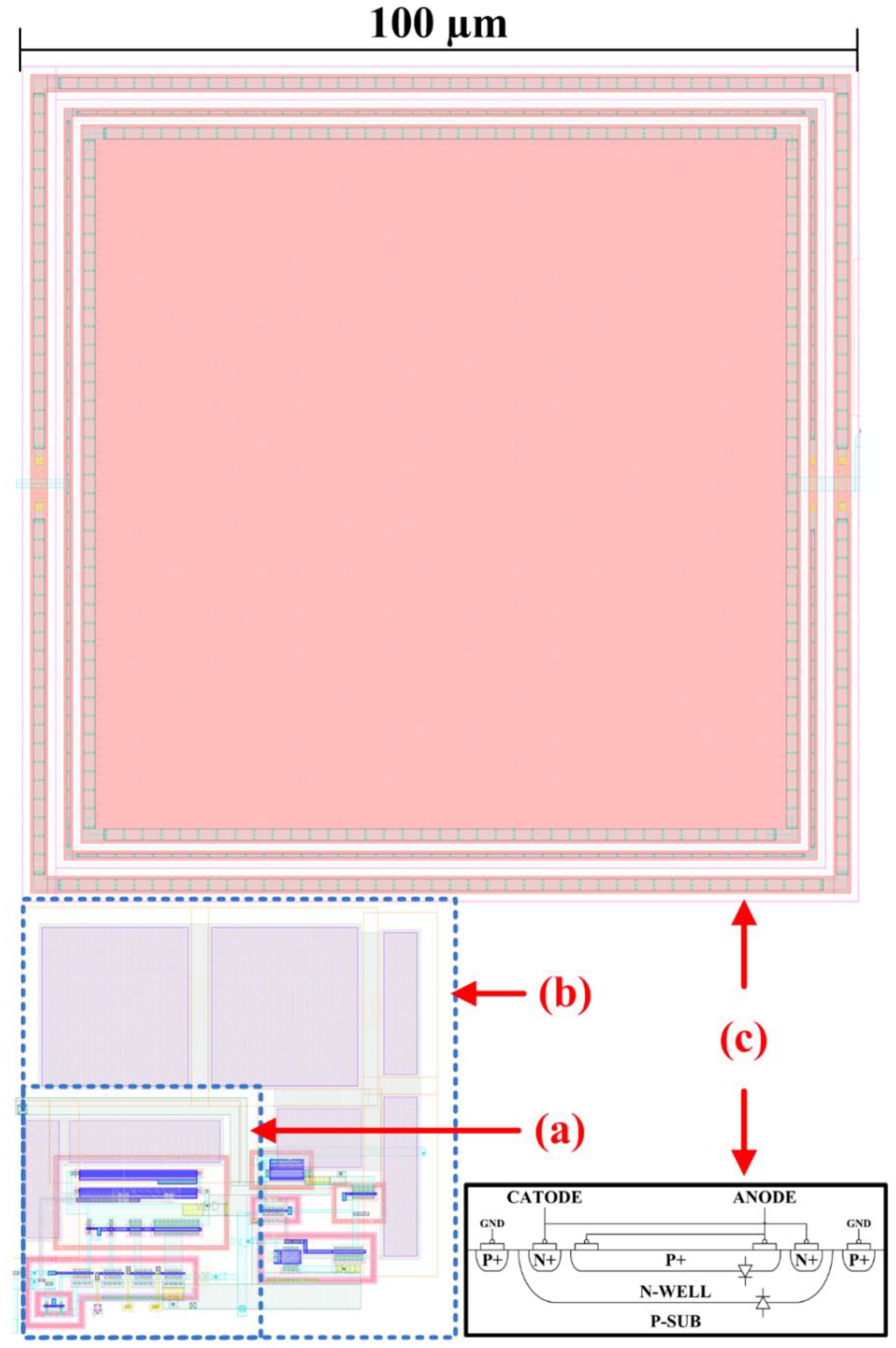
Figure 3 shows the complete layout of the optoelectronic sensing system designed in standard TSMC 0.18 μm CMOS technology. The TCG stage and the CVC stage, composing the TIA, are shown in panels (a) and (b), respectively, and require a total Si area of 2070 µm
2. Moreover, panel (c) shows the integrated square PD based on a PNP junction with a Si area of 10,000 µm
2. In the inset of
Figure 3, the PD cross section highlighting the main parts of this device implemented by using the CMOS technology standard layers is reported. The size of the PD sensitive area has been chosen to guarantee a small junction capacitance
CJ (about 8 pF) and standard values of shunt
RSH (higher than 100 MΩ) and in-series
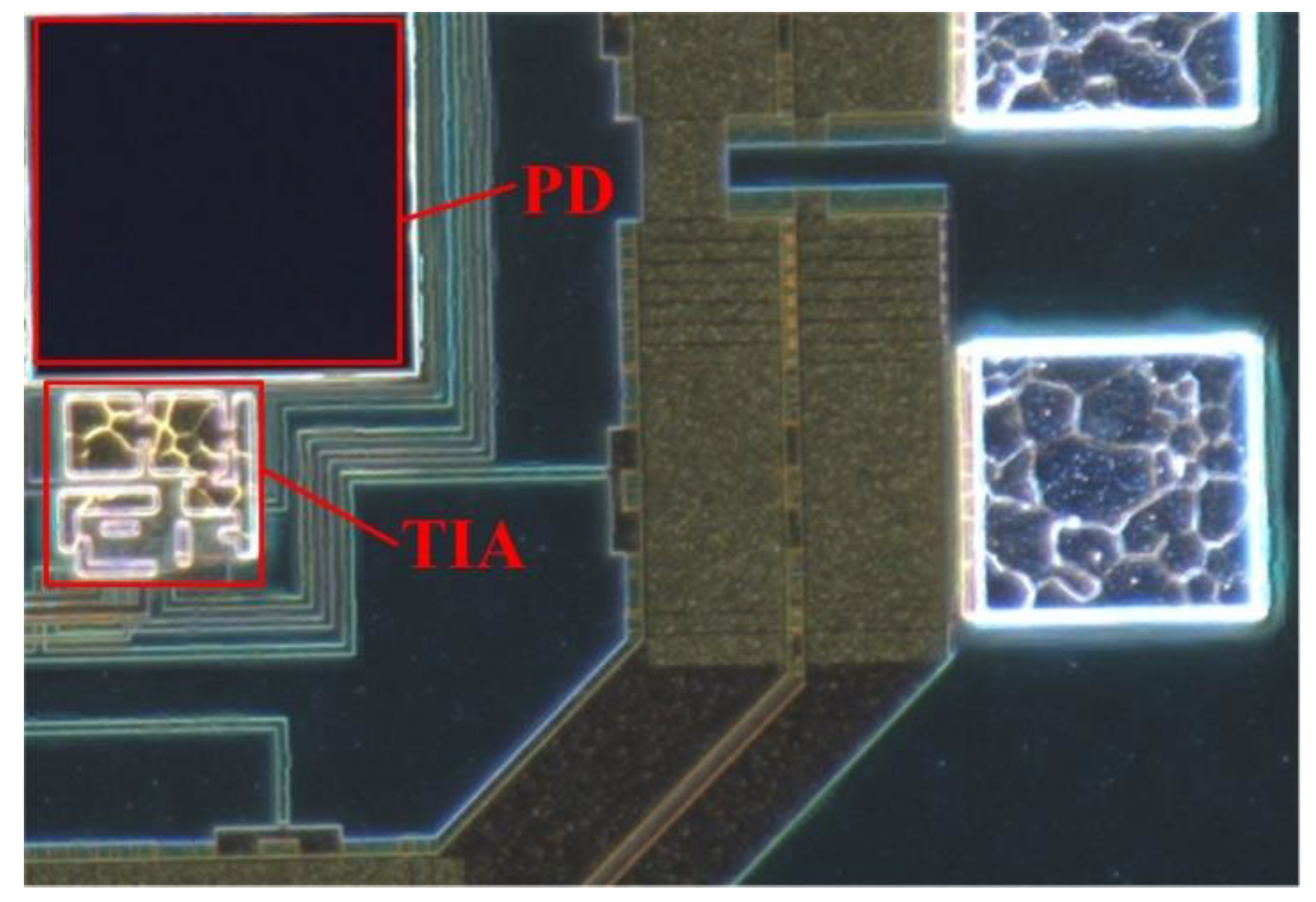
RS (about 50 Ω) resistances to make this device suitable to detect light pulses for optical biomedical applications. A microphotograph of the fabricated and integrated SoC (i.e., the overall ASIC) is shown in
Figure 4.
3. Experimental Results: Characterization and Validation
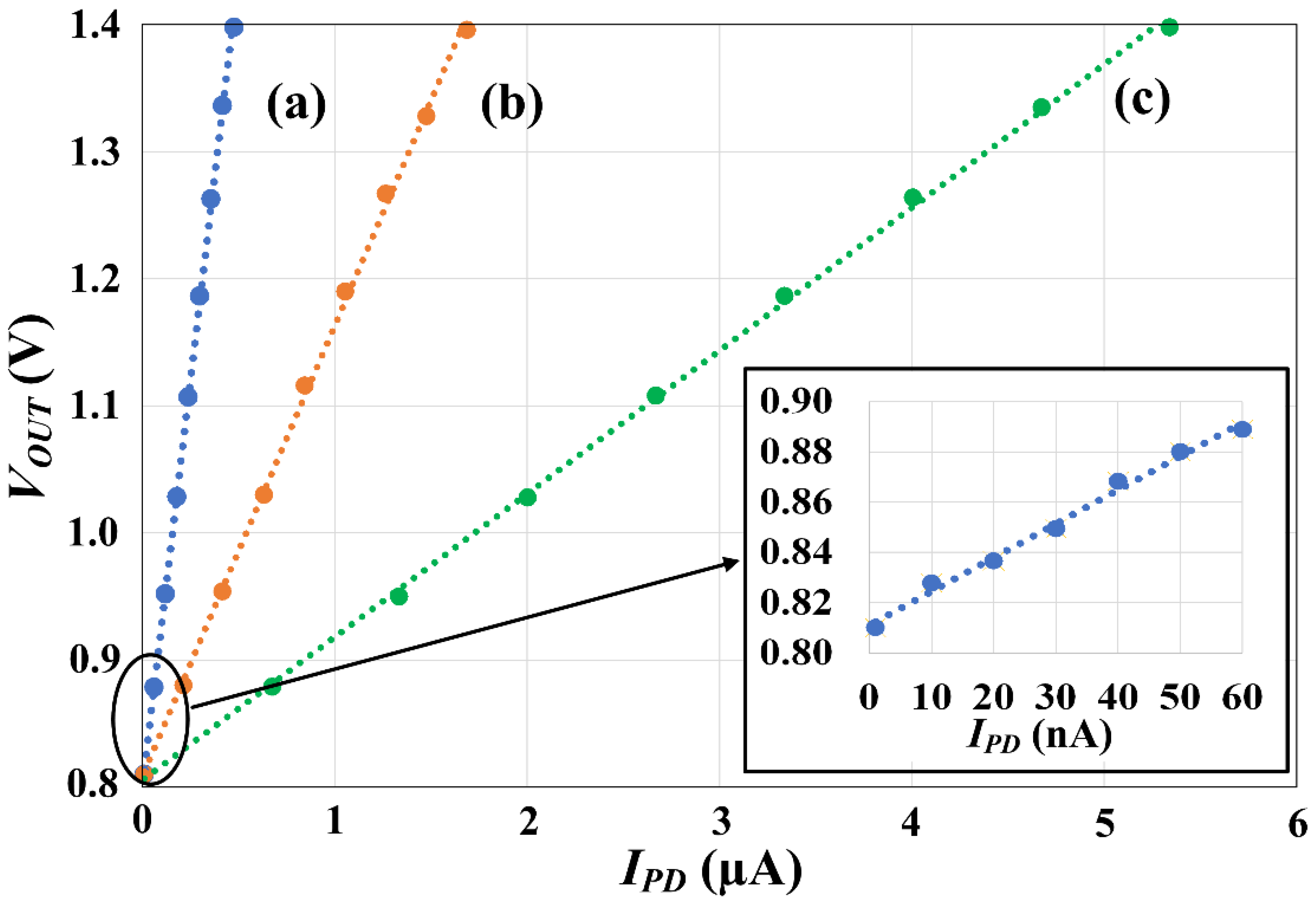
The electrical characterization of the fabricated CMOS integrated optoelectronic sensing SoC has been performed, first excluding the internal Si PD, to analyze the electronic response of the TIA only. Referring to
Figure 2, for performing this method, the photocurrent
IPD has been achieved through a voltage source connected to the TCG stage input in a series with a 1 MΩ resistor. In this regard,
Figure 5 shows the measured TIA output voltage
VOUT as a function of the input photocurrent
IPD under DC operating conditions (i.e., the TIA DC sweep analysis), which is achieved by varying the amplitude of the input voltage source. By fixing the analog control voltage
VAN = 1.8 V, it has been obtained: plot (a) the maximum TIA transimpedance gain equal to 1.41 MΩ (123 dbΩ by setting the digital control voltages equal to
V1 =
V2 = 0 V and
V3 = 1.8 V; plot (b) the intermediate TIA transimpedance gain equal to 398 kΩ (112 dbΩ) by setting
V1 =
V3 = 0 V and
V2 = 1.8 V; plot (c) the minimum TIA transimpedance gain equal to 126 kΩ (102 dBΩ) by setting
V2 =
V3 = 0 V and
V1 = 1.8 V. In the inset of
Figure 5 a magnification of the DC sweep analysis for the maximum achieved TIA gain of 123 dbΩ is reported considering the input current
IPD ranging from 2 nA to 60 nA with a resulting maximum linearity error lower than ±0.5%. For these three operating conditions, the linear fitting procedures of the experimental data (i.e., the dotted lines in
Figure 5) demonstrate that the TIA response is always linear with respect to the reported variation in the
IPD input current. The measured TIA voltage offset (i.e., the minimum
VOUT level) was about 0.81 V corresponding to a minimum input current
IPD of about 2 nA: a value close to the typical dark current level of Si PDs. However, this offset level strictly depends on the design (i.e., the sizing) and the operating point of the CVC stage, while the results, in order to be independent of the TCG stage, gain set by the control voltages
V1,
V2,
V3, and
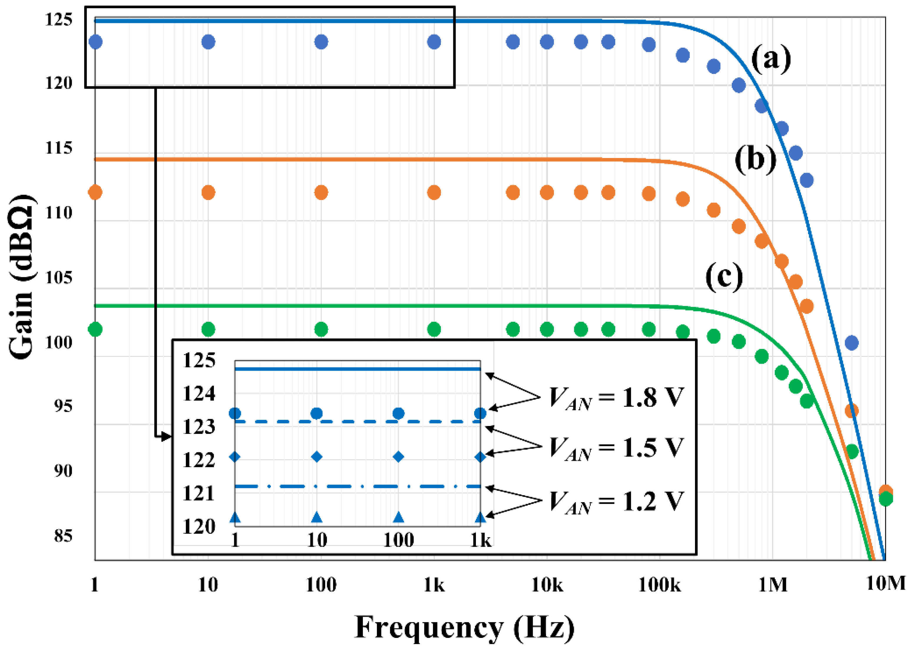
VAN. Furthermore, the maximum power consumption of the TIA has been evaluated to be about 54 µW. Then, the TIA frequency response (i.e., the TIA AC sweep analysis) is performed by employing an arbitrary waveform generator (GD1032Z by RIGOL) to provide a 100 nA sinusoidal input current signal at different frequencies. In this regard,
Figure 6 reports the measured AC sweep response of the TIA, where the continuous lines have been obtained from the theoretical analysis using Equation (1), and the dots are the experimental data achieved for the different transimpedance gains. Under the same operating conditions for the analog and digital control voltages of the DC sweep analysis reported in
Figure 5, in
Figure 6, plot (a) confirms the maximum transimpedance gain of about 123 dBΩ and a bandwidth of about 500 kHz; plot (b) reaches the intermediate transimpedance gain of 112 dBΩ and a bandwidth of about 600 kHz; plot (c) presents a minimum transimpedance gain of 102 dBΩ and a bandwidth of about 1.1 MHz. The inset of
Figure 6 reports the variations of a few dBΩ of the maximum achievable transimpedance gain of 123 dBΩ for three different values of the voltage
VAN: for
VAN = 1.8 V where the continuous line and the dots are the theoretical transimpedance gain and the experimental data, respectively. For
VAN = 1.5 V, the dashed line and the diamonds are the theoretical transimpedance gain and the experimental data, respectively; for
VAN = 1.2 V, the dot-dashed line and the triangles are the theoretical transimpedance gain and the experimental data, respectively. Moreover, in order to complete the electrical characterization of the circuit, experimental measurements of the Total Harmonic Distortion (THD) have been performed and obtained a maximum value of about 4.6%, within the TIA bandwidth, at about
VOUT = 590 mV
PP, which was obtained with an input current
IPD of about 440 nA and a maximum transimpedance gain of about 123 dBΩ (refer to the plot (a) of
Figure 5).
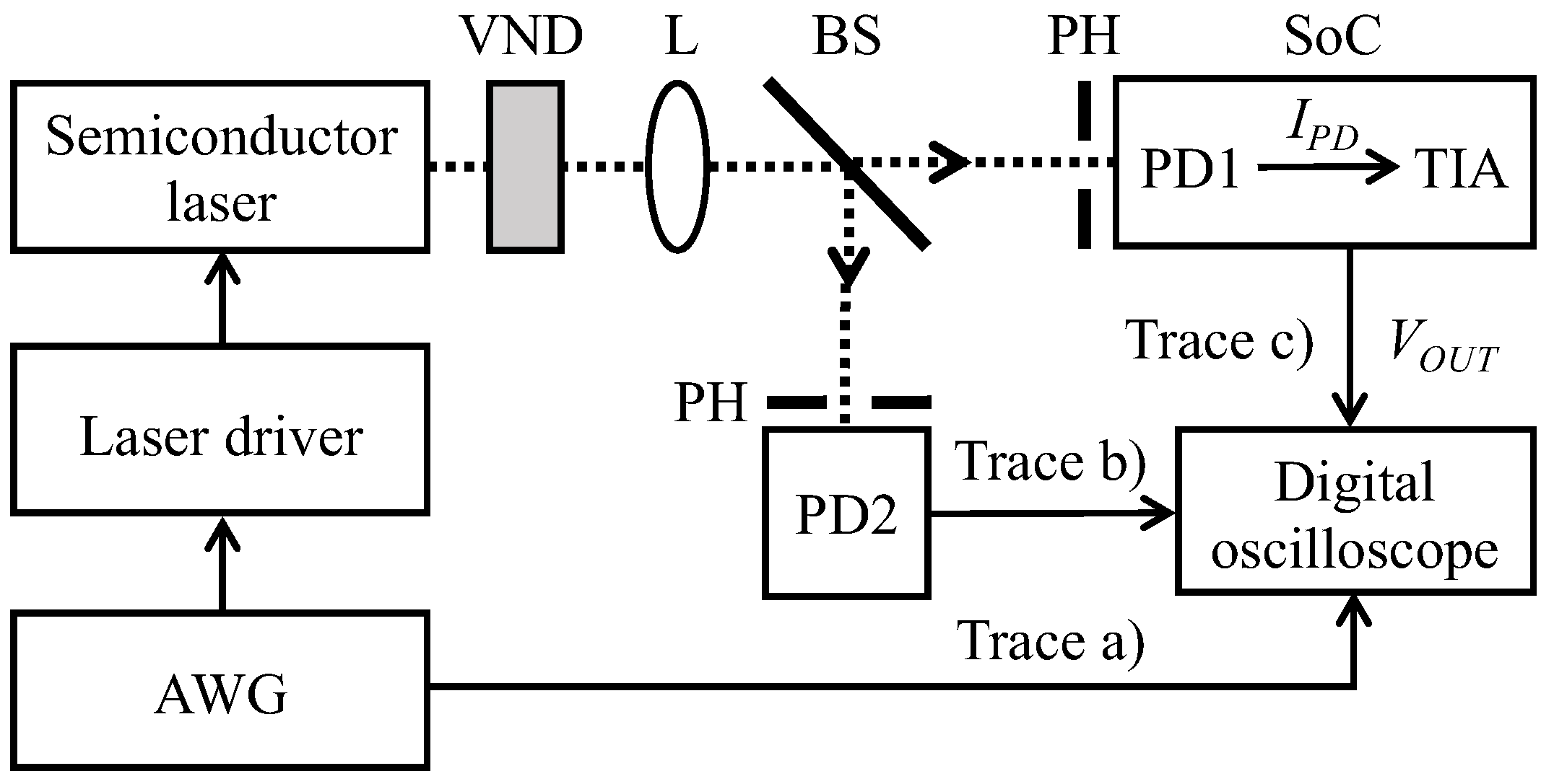
Once the TIA electrical responses have been experimentally verified, a series of measurements are also performed to determine the performances and the characteristics of the whole optoelectronic sensing SoC (i.e., the integrated Si PD and the TIA) by employing the experimental setup reported in
Figure 7. In particular, the laser beam generated by a semiconductor laser emitting at λ = 633 nm (HL63163DG driven by its temperature controller and driver LDM56/M by Thorlabs) passes through a variable neutral density filter, VND, which is suitably used to vary its transmitted power. The laser beam is collimated and focused by means of an optical lens system, L, before being divided into two optical paths of the same length by a 1 mm thick 50/50 beam slitter at the laser emission wavelength (BSW10R by Thorlabs). At the end of one of these paths is located the PD2, a calibrated Si PD (FDS100-CAL by Thorlabs) with its own responsivity, in terms of Ampere/Watt (A/W), of about 0.31 A/W @ λ = 633 nm. This allows for the determination, indirectly, of the effective power of the laser beam impinging on the PD2 sensitive area by measuring the generated voltage across the load resistor provided by the input impedance of the employed oscilloscope (i.e., 1 MΩ). The knowledge of laser power is, in fact, the main parameter for the optical characterization of the fabricated optoelectronic sensing SoC. The SoC built-in PD, and PD1 in
Figure 7, are located at the end of the other optical path. PD1 generates a photocurrent proportional to the light intensity illuminating its sensitive area, that is, the input current
IPD of the TIA. Since the sensitive areas of PD1 and PD2 are different, a pinhole, PH, with a diameter of 100 μm (PV100 by Thorlabs) and equal to the side of the PD1 square sensitive area (see
Figure 3), was positioned in front of each one of the employed PDs. Moreover, to achieve the best optical alignment respective of the PD1 and PD2 sensitive areas, the two pinholes have been mounted on an XYZ micrometer translational stage. This procedure ensures that both PD1 and PD2 are illuminated by the same amount of light power carried by the laser beam gently focused on the pinhole surfaces by the L optical lens system. In
Figure 7, AWG is the same arbitrary waveform generator (GD1032Z by RIGOL) used for the AC sweep analysis in
Figure 6 that is used in the following for the time domain optical characterization of the optoelectronic sensing SoC together with a digital oscilloscope (DLM2034 by Yokogawa). The first step in the optical performance’s evaluation of the fabricated SoC is proceeded under a continuous wave operation of the laser emission and, referring to the setup of
Figure 7, the experimental data have been obtained by using a digital multimeter (i.e., Agilent 34401 digital multimeter) replacing the digital oscilloscope.
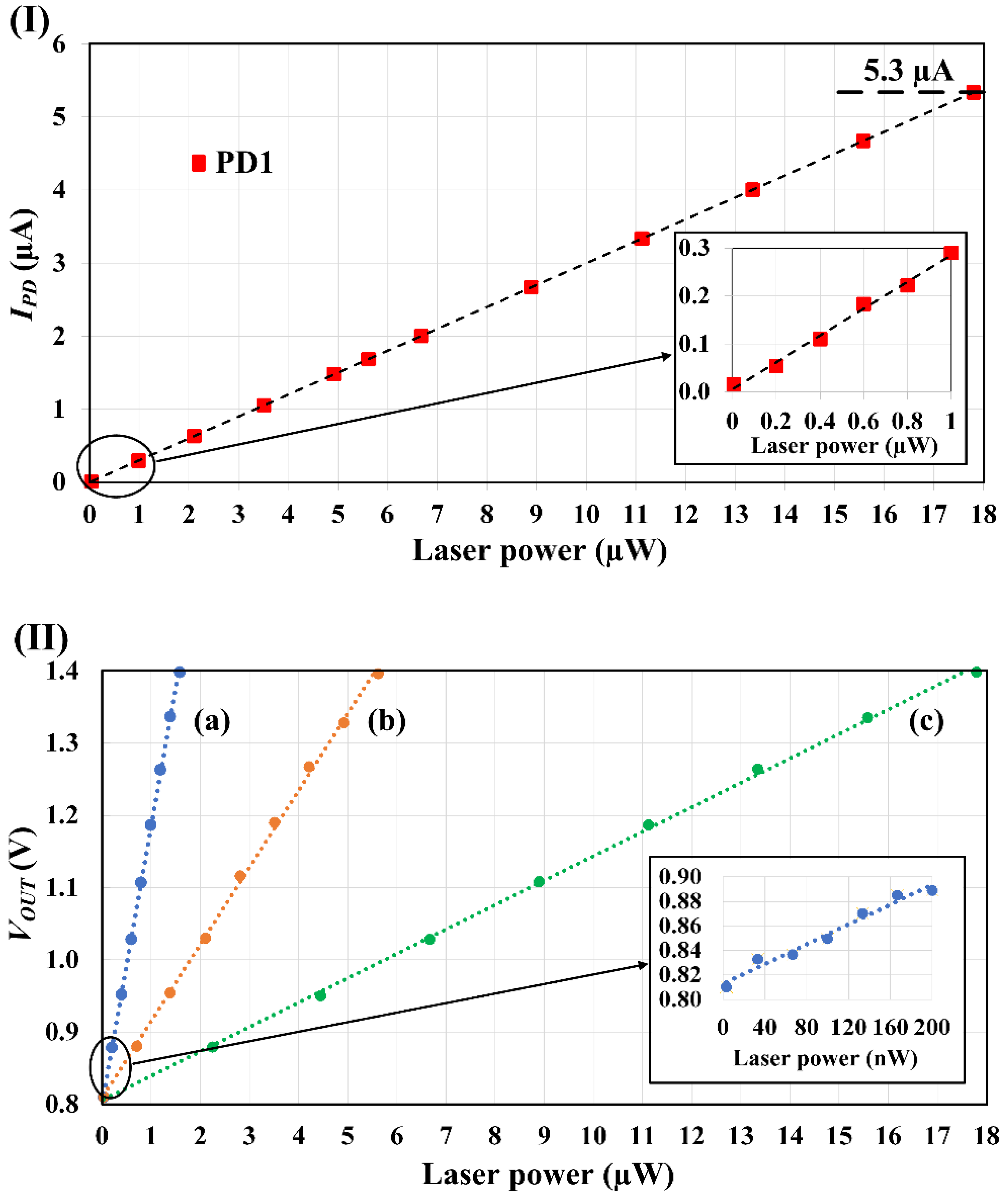
Figure 8I shows the measured photocurrent
IPD generated by PD1 as a function of the incident laser power detected by PD2 (see
Figure 7). For the reported range of the variation in the laser power, the PD1 linear response is demonstrated by the linear fitting procedure of the experimental data and indicated by the dashed line. This allows for the definition of the responsivity of the integrated PD1 on the fabricated SoC: a key parameter characterizing any photodiode. In the present case, the achieved PD1 responsivity at the laser emission wavelength is about 0.3 A/W, a value comparable with those of the commercial Si PDs [
32]. In
Figure 8II, it is reported that the SoC output voltage
VOUT is a function of the incident laser power for the same three values of the transimpedance gains of
Figure 5 and
Figure 6. The data reported in
Figure 8II are limited to those values of
VOUT for which the system response is linear (i.e.,
VOUT ranging from 0.81 V to about 1.40 V). In this case, the TIA input current is the one generated by the integrated PD1 (i.e.,
IPD) and connected to the TIA, according to
Figure 7. In particular, in
Figure 8II, plots (a), (b), and (c) have been obtained by setting the transimpedance gains equal to 123, 112, and 102 dBΩ, respectively. The dashed lines are the results of the linear fitting of the experimental data. Moreover, the inset of
Figure 8I reports the generated PD1 current
IPD, considering an incident laser power varying from 1 nW up to 1 µW, showing a maximum linearity error lower than ±0.5%. In addition, the inset of
Figure 8II shows the SoC output voltage
VOUT, for the maximum transimpedance gain of about 123 dBΩ, as a function of the laser power ranging from 1 nW up to 200 nW with a corresponding maximum linearity error lower than ±1%.
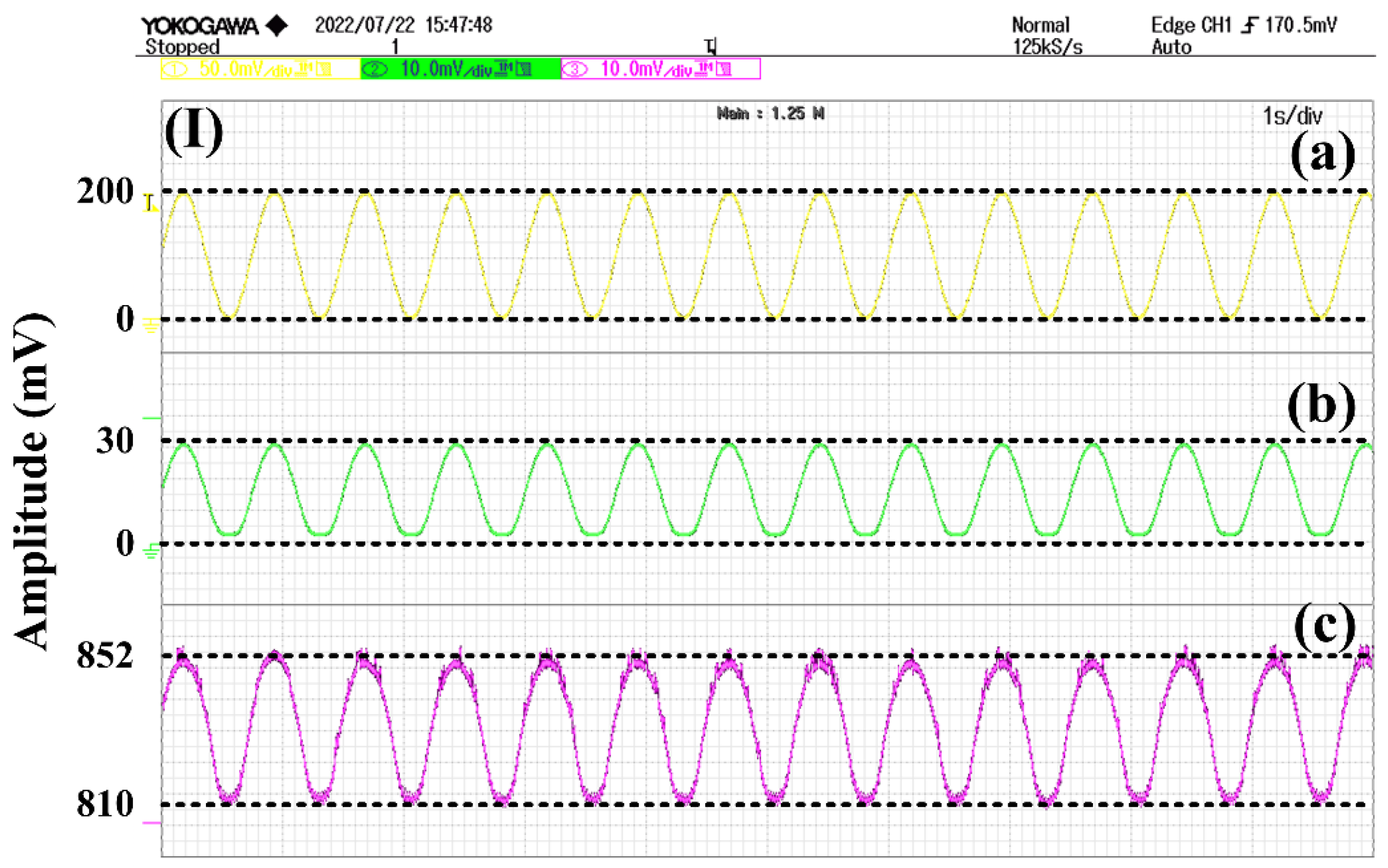
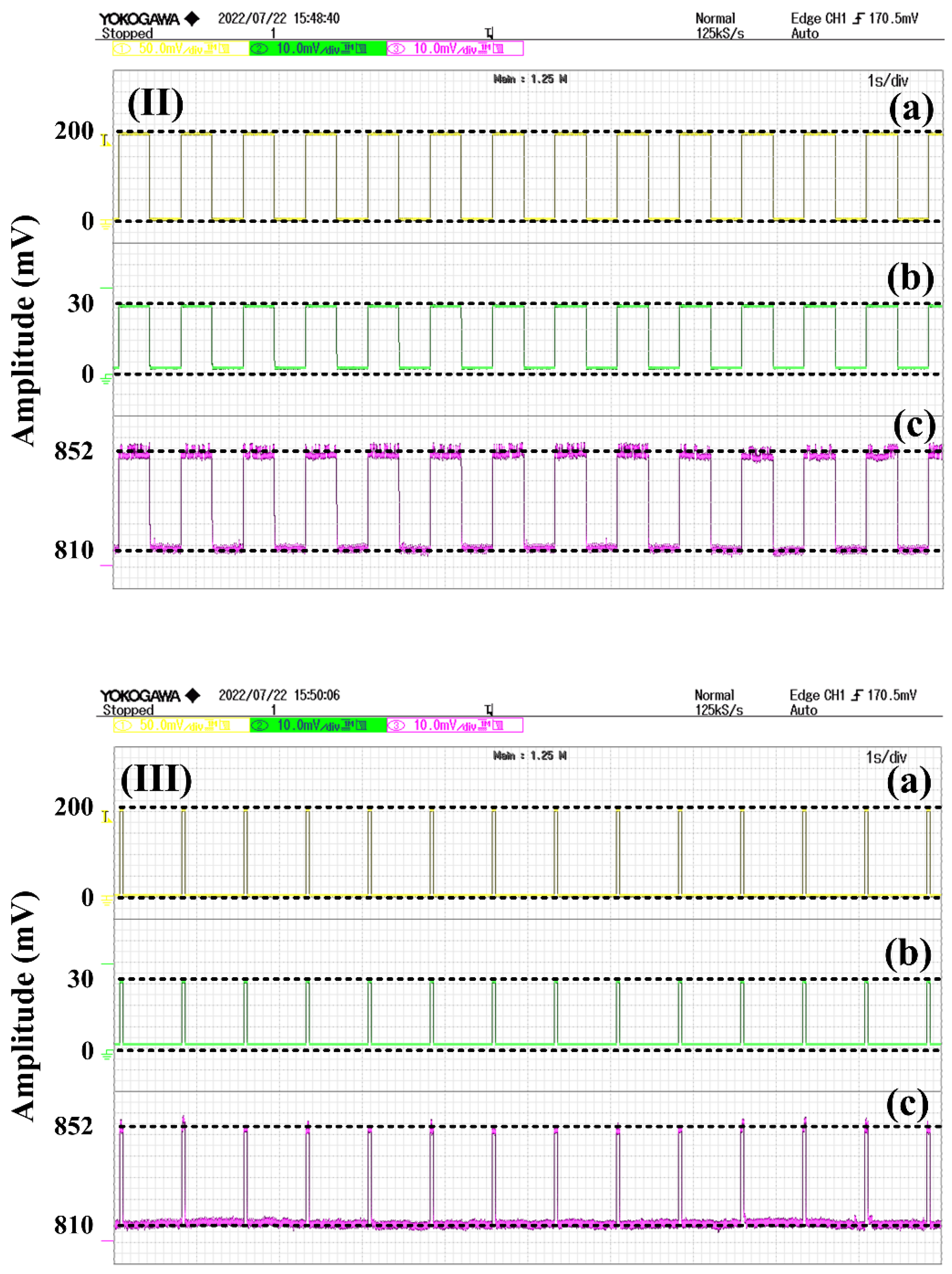
Furthermore, the time-domain characterization of the optoelectronic sensing SoC has been performed by employing a laser beam whose power is periodically modulated by using the AWG connected to the laser driver (see
Figure 7). Thus, once a specific waveform is generated by the AWG, its output is connected to the laser driver, and the resulting power of the emitted laser beam follows the electrical modulating waveform (i.e., the generated laser beam power is an optical replica of the electrical waveform applied to the laser driver). Considering the characteristics and specifications/features of the typical biomedical signals, the chosen periodic AWG waveforms have a frequency equal to 1.3 Hz and a maximum voltage amplitude equal to 200 mV. As shown in
Figure 9, the time-domain characterization of the optoelectronic sensing SoC has been performed by using: in
Figure 9I, a sinusoidal waveform; in
Figure 9II, a square waveform; and in
Figure 9III, a periodic sequence of pulses. Referring to
Figure 7, each panel of
Figure 9 reports the following digital oscilloscope signals: trace (a) the AWG modulating signal applied to the laser driver; trace (b) the modulated laser beam power detected by PD2 (i.e., the optical replica of the AWG modulating waveform); this voltage signal has a maximum amplitude of about 30 mV corresponding to a photocurrent
IPD ≅ 30 nA generated by the PD2 connected to the 1 MΩ input of the digital oscilloscope; trace (c) has an SoC output voltage
VOUT with a maximum amplitude of about 42 mV. Considering that the TIA is operating at its maximum transimpedance gain equal to 123 dBΩ (i.e., 1.41 MΩ), the above-measured
VOUT is in good agreement with the data determined from the DC and AC sweep analyses of
Figure 5 and
Figure 6, as well as with the results of
Figure 8. Moreover, it is important to consider that, in all these cases, the presented saturation/distortion effects on the waveforms are not introduced by the electronic system due to the saturation/distortion phenomena introduced directly by the laser driver (i.e., the effects due to the laser biasing variations and the fluctuations of the output laser power as well as the temperature drift of the semiconductor laser source).
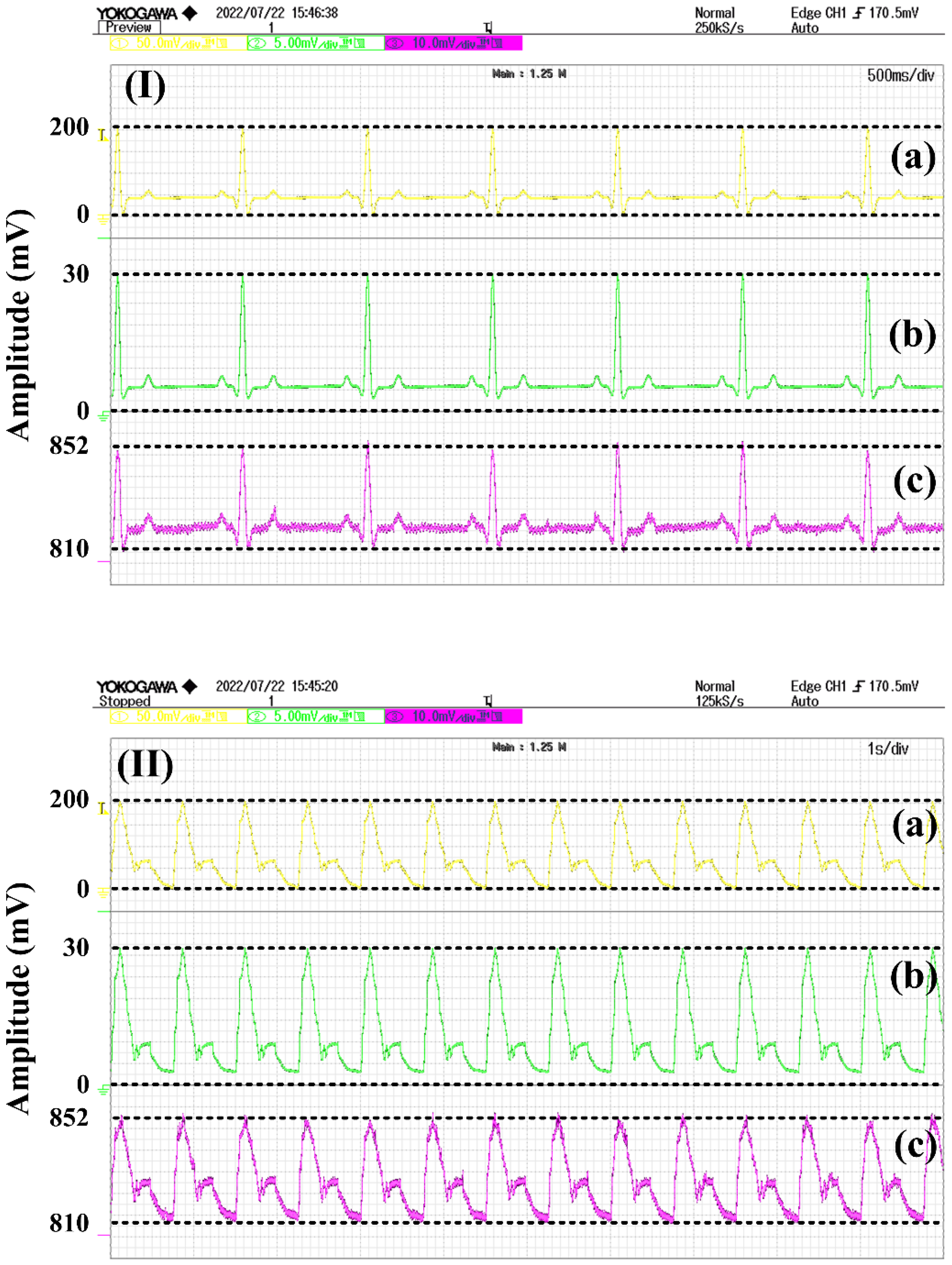
As case examples of biomedical applications, the developed optoelectronic sensing Soc has been also employed to detect typical ECG and PPG signal patterns [
9,
33]. These signals have been emulated through the AWG that has been suitably configured to generate standard biomedical signals at a repetition rate of 1.3 Hz (corresponding to about 46 beats per minute) with a maximum output voltage of 200 mV. Following the previous procedure and referring to
Figure 7, the AWG-generated ECG and PPG signals have been used to modulate the laser beam power so as to provide the optical replica of the two considered electrical stimuli. In
Figure 10I,II the digital oscilloscope traces achieved by employing the ECG and PPG signal patterns are reported, respectively. In both the two panels of
Figure 10, the digital oscilloscope traces (a) are the AWG-generated biomedical patterns modulating the laser beam power, traces (b) are the optical replicas of traces (a) detected by the PD2 (see
Figure 7) with a maximum amplitude of about 30 mV corresponding to a photocurrent
IPD ≅ 30 nA, and trances (c) are the SoC output voltages
VOUT with a maximum amplitude of about 42 mV. Additionally, in these last cases, considering that the TIA is operating at its maximum transimpedance gain equal to 123 dBΩ (i.e., 1.41 MΩ), the above measured
VOUT is in good agreement with all the previously reported data in
Figure 5,
Figure 6 and
Figure 8. In other words, the achieved results demonstrate the capability of the fabricated optoelectronic sensing SoC to properly process and amplify the optical biomedical signals, reproducing all the features of typical ECG and PPG standard patterns.
Finally, in
Table 2, the main characteristics and performances achieved by the proposed optoelectronic sensing SoC are summarized and compared with those ones of similar solutions for biomedical applications reported in the literature. The proposed system requires the smallest Si area and lower power consumption and operates with different input waveforms, always achieving high transimpedance gain and bandwidth and presents the best value of figure of merit (FOM), which is defined as the product of the transimpedance gain by the bandwidth divided by the power consumption (i.e., in units of ΩxGHz/mW).


 ,
, 


