Article

Novel Planar Ultra-Wideband Modular Antenna Array with Low Profile

1
College of Electronic Science and Engineering, National University of Defense Technology, Changsha 410073, China
2
54th Research Institute, China Electronics Technology Group Corporation, Shijiazhuang 050081, China
3
College of Advanced Interdisciplinary Studies, National University of Defense Technology, Changsha 410073, China
4
School of Electronic and Information Engineering, South China University of Technology, Guangzhou 510641, China
*
Author to whom correspondence should be addressed.
Electronics 2022, 11(24), 4173; https://doi.org/10.3390/electronics11244173
Submission received: 19 November 2022 / Revised: 5 December 2022 / Accepted: 7 December 2022 / Published: 14 December 2022

Abstract

:
A planar ultra-wideband modular antenna array with an ultra-low profile based on a tight coupling effect is proposed. The antenna array is composed of multi-layer printed circuit boards. Since its frequency operation can extend up to the grading lobe frequency, the number of T/R components for the antenna aperture is reduced to the greatest extent. Specifically, a horizontal “fin” structure is added on the parallel feeding lines, which assists in improving the impedance matching of the array. In order to break the bandwidth limitation of the low-frequency loop mode, a capacitive short-circuit probe is introduced to push the common-mode resonance point into the low-frequency band. Finally, subject to Active VSWR < 3, the array can realize E-plane, H-plane, and D-plane ± 45° beam scan coverage across the 6:1 frequency band (3.48–20.97 GHz). A 128-element prototype was processed and tested to validate the design. This array not only has the advantages of low profile, modularity, easy assembly, and maintenance but also minimizes the number of T/R components and reduces the cost of phased array antennas.

1. Introduction

Ultrawideband and wide-scan phased array antenna refers to the electronically scanned antenna array covering a wide working frequency band and elevation angle scanning range of at least ±45°. They are usually featured with polarization agility and wide-scan performance, thus playing an increasingly important role in high-throughput wireless communication systems that demand wideband beamforming front ends, including sensing systems, multifunctional RF systems, electronic countermeasures, and radio telescope, [1,2,3,4].
The Vivaldi array is one of the most popular types of wideband arrays, and research shows that they are capable of 10:1 bandwidth [5,6]. However, to attain wide bandwidth performance, the profile of Vivaldi arrays has to be fairly high, commonly 2–3λ at the highest working frequency [7]. In addition to the height, Vivaldi arrays also suffer from high cross-polarization when scanning, which is induced by the vertical current running down the length of the feeding structure that is perpendicular to the array plane [8]. Therefore, their high profile and poor polarization purity limit their application to certain platforms.
Tightly coupled dipole arrays (TCDAs) technology is one of the implementations of Wheeler’s current sheet concept that an infinite periodic array of closed-arranged dipoles can support currents at wavelengths that are much larger than the dimension of a single element [9,10,11], as shown in Figure 1a. Munk suggested that for an array in which the elements are arranged closely to take advantage of capacity coupling from adjacent elements, the inductance introduced by the ground plate will be compensated so that the array will have excellent bandwidth and scanning performance, as shown in Figure 1c [12,13]. It is expected to be an alternative low-profile wideband array technology that overcomes the limitations of the Vivaldi array. TCDA has received widespread attention and has developed rapidly in the past two decades since the first prototype of TCDA was published in 2003 [14,15,16,17,18]. Among these proposed schemes, the planar ultra-wideband modular antenna (PUMA) array is the most appealing one due to its simplicity, modularity, high integration, and ultra-low profile [19,20,21,22,23]. Different from other TCDAs, the PUMA array can be manufactured with a low-cost multilayer PCB fabrication process without using external baluns and feed organizers [13]. The first generation of PUMA arrays showed great performance across the frequency band of 7–21 GHz [19]. To obtain band-width ratios (BWR = fhigh/flow:1) of 5:1, a planar matching circuit on the backplate was brought in; however, the design was only validated via simulation [20]. The latest PUMA realized 6:1 BWR, utilizing a vertically oriented impedance matching structure, but the height above the ground increased to 0.48λhigh (wavelength at the highest working frequency) [21].
In the primary stage of TCDA design, the equivalent circuit method could be employed to calculate and optimize some key parameters of the structure, including the distance between dipoles and the metal ground plate and the capacitive coupling of the adjacent elements. Generally, feeding structures are ignored temporally, and discrete ports are used as excitation for the array. After that, a full-wave simulation would be carried out for the combination of the dipole and the feeding structure to obtain more parameters of the design. Take advantage of the development of an optimization algorithm, this multi-objective optimization process could be simplified and highly efficient.
In this paper, a novel PUMA array working over 3.48–20.97 GHz is proposed. Because its frequency operation can extend up to the grading lobe frequency, only a small number of T/R components for the antenna aperture is needed. Specifically, a horizontal “fin” structure is added on the parallel feeding lines, which assists in improving the impedance matching of the array. In order to break the bandwidth limitation of the low-frequency loop mode, a capacitive short-circuit probe is introduced to push the common-mode resonance point into the low-frequency band. Subject to Active VSWR < 3, the array can realize E-plane, H-plane, and D-plane ±45° beam scan coverage across the 6:1 frequency band. A 128-element prototype was fabricated and tested to validate the design.

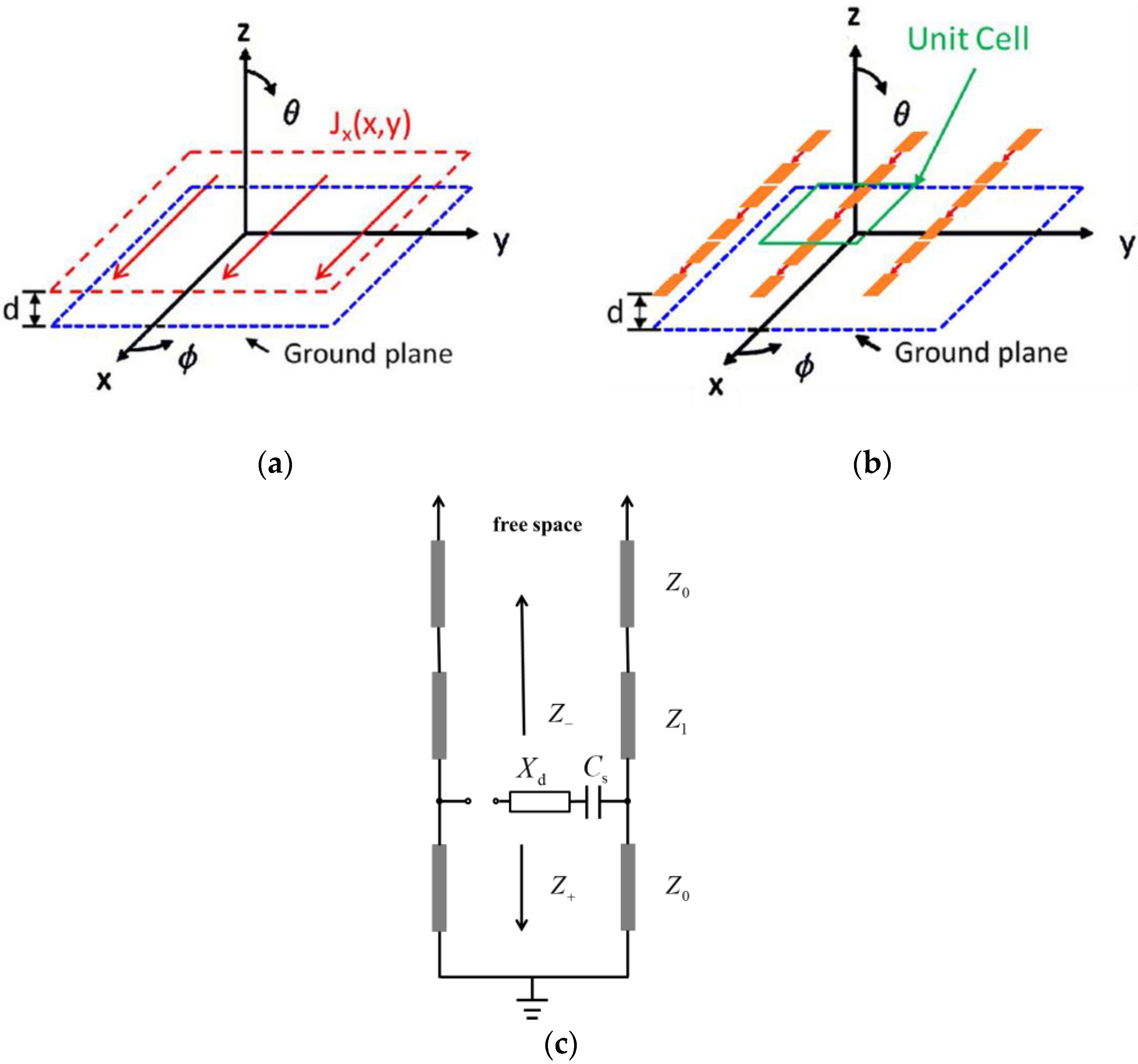
2. Structure of the Proposed PUMA

The proposed PMUA structure is shown in Figure 2. Similar to previous PUMA arrays, the dual polarized dipole segments are fed directly with parallel lines, in which one line connects to an external feeding structure while another line is grounded. To minimize the vertical current that is induced by this unbalanced feeding structure, the dipole configuration is asymmetrical, and the fed dipole arm is 20% larger than the grounded arm. A center circular patch is located at the end of the dipole antenna in favor of enhancing coupling capacitance between dipoles printed on the same layer. Beneath the dipole arms is a metallic coupling patch etched on the substrate layer, and the patch is grounded via a shorting probe, which provides the necessary capacitance to the radiators so as to remove the common-mode that appears within the operating band. To reinforce the effect, the shorting probe is offset from the center of the coupling patch. Two pairs of fin structures are loaded onto feeding lines, offering additional capacitance to the transmission line.
Two substrates are introduced as cover layers on the dipoles, enabling better impedance transition between the array and free space. Substrates also serve as a wide-angle impedance matching layer, improving array scanning performance. Multiple layers of substrate between the ground and dipoles provide the feeding lines and grounded connections with mechanical support, and to prevent the occurrence of surface waves, low permittivity PTFE is chosen for these dielectric stackup. The bottom of the substrate layer is clad with metal, enabling the bonding between the substrate layers and the ground, which host a vertically oriented coaxial impedance transformer linking to a standard 50 Ω source. In practice, the transformer section can be integrated with SSMP.
The PUMA arrays have a 0.46λhigh aggregate thickness above the ground, which is thinner than that of the array proposed in [23]. Like its predecessors, this PUMA array is perforated with cylindrical holes through entire multiple PCB layers; this reduces the effective permittivity of the superstrate and substrate, avoiding unwanted surface waves caused by thick dielectric layers. On the other side, drilling lightens the weight of the entire PUMA array.
The structure geometric parameters and dielectric parameters are listed in Table 1 and Table 2, respectively.
The proposed PUMA array is fabricated, and the prototypes are presented in Figure 3. Each array includes 128 elements (256 ports in sum). Previously, it has been demonstrated that several PUMA arrays of the same type can be joined together in a modular manner, as shown in Figure 3b. In addition to multilayer PCB welded on a copper ground plate, the backplate contains 16 sub modular tiles hosting 4 × 4 cylindrical holes fitted with 50 Ω male push on connectors with flexible probes alignmed with feeding lines of array elements. These tiles are fixed to the ground plate with machine screws; in this way, flexible probes can be compressed and a reliable electrical connection can be made between the array feeding lines and the tile connectors. This modular feed fashion has an obvious advantage over the first generation of PUMA that was mounted on an expander measurement fixture; it is not only more favorable for rapid construction of prototypes, but also provides tremendous convenience for later maintenance because of its high degree of reliability as well as repeatability.

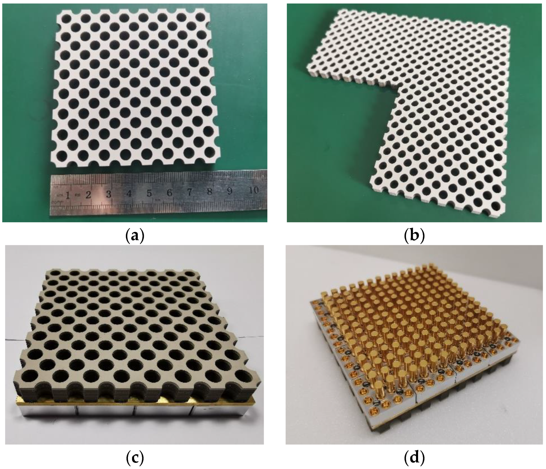
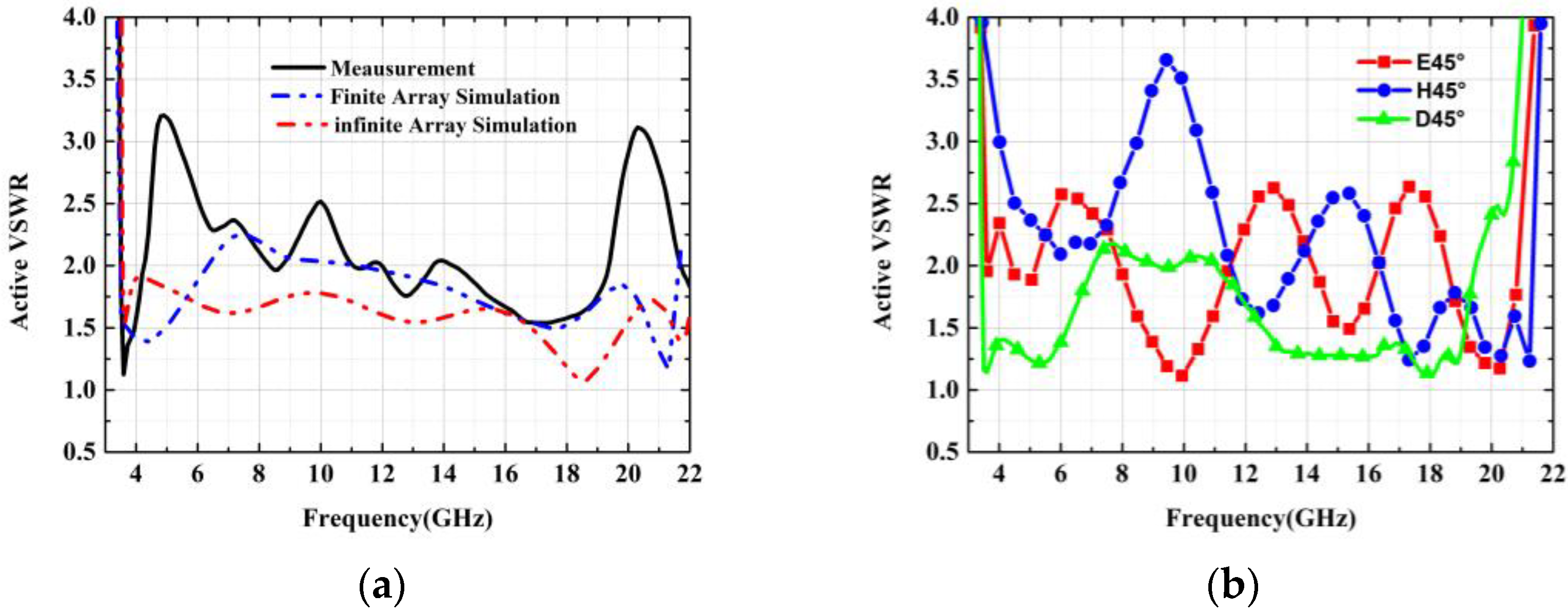
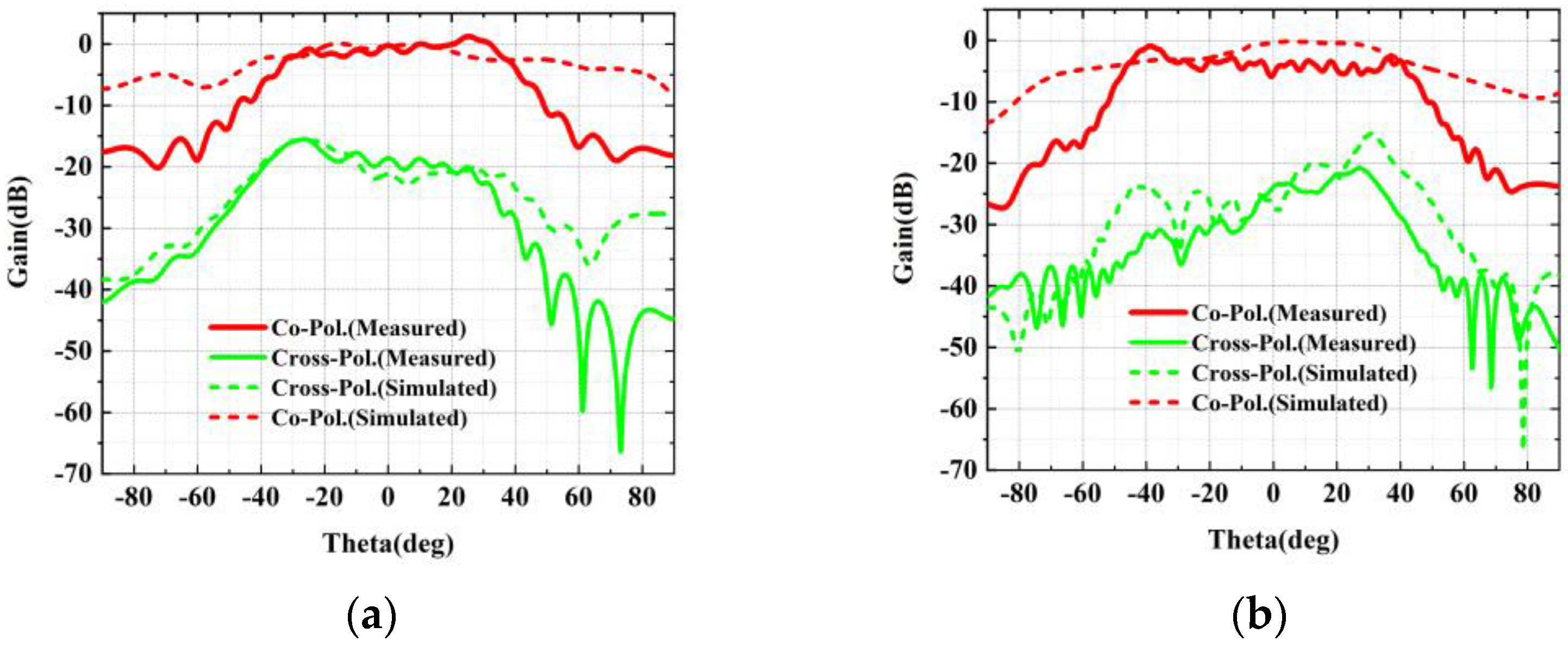
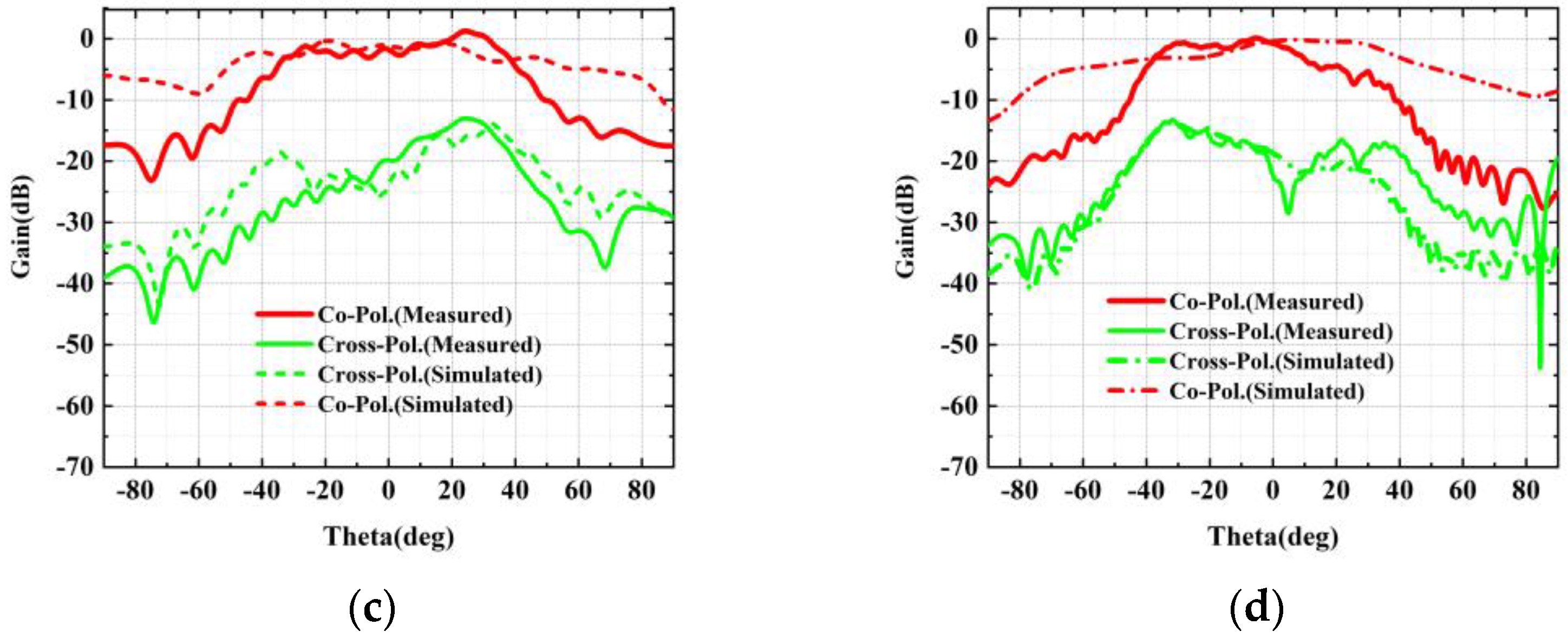
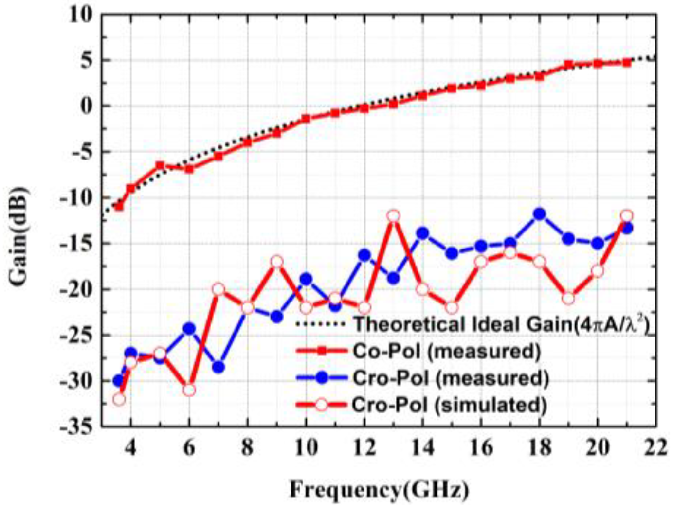
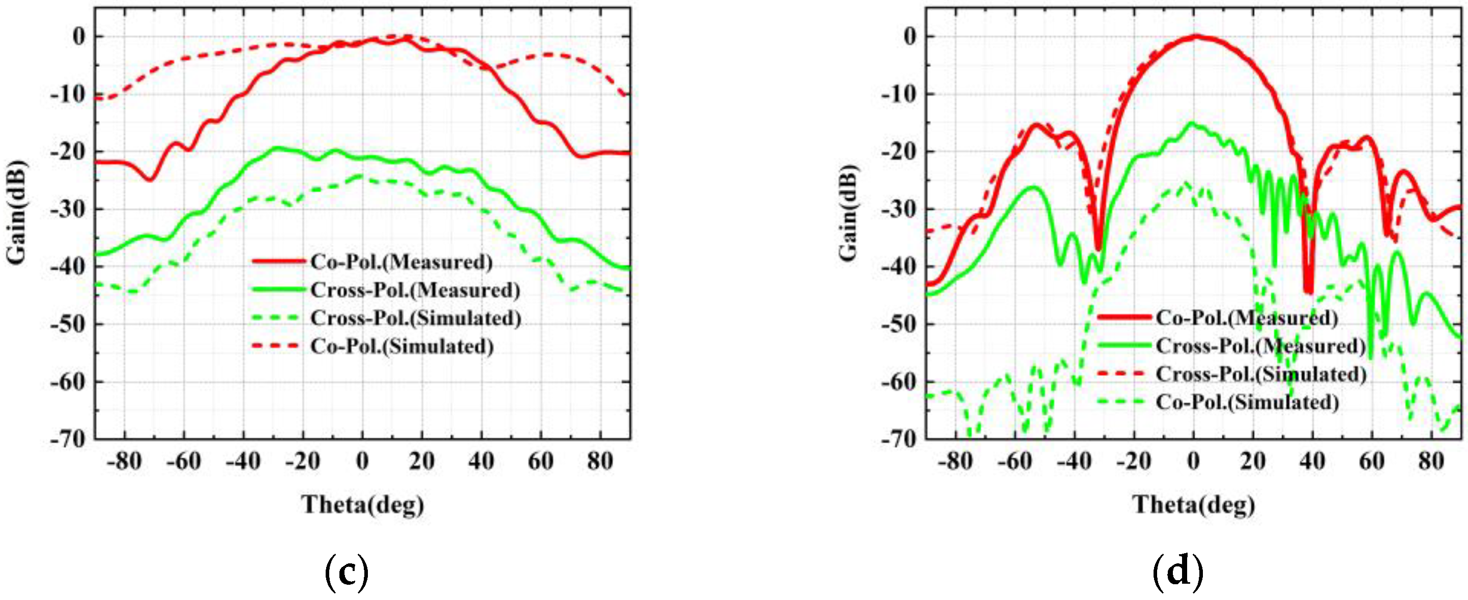
3. Measurements and Validation

The element in the center of a larger array is supposed to have similar impedance characteristics as that of an infinite array. For dual-polarized arrays, the measurement of active S-parameters must consider the contribution of mutual coupling from elements of the same polarization direction, while all elements of the orthogonal polarization direction are matched. The array is assumed to be excited with uniform amplitude, and the active reflection coefficient of element (p,q) can be given by the following expression [24,25,26]:
Γ p q ( θ , ϕ ) = m = 1 M n = 1 N S n m , p q e j [ ( m p ) D x u + ( n q ) D y v ]
where ( θ , ϕ ) indicates array scan direction, u = k sin θ cos ϕ , v = k sin θ sin ϕ and they represent uv coordinates respectively. Parameter k is the wavenumber in free space, Snm,pq is the transmission coefficient between elements mn and pq, and Dx and Dy are the lattice spacing in the x and y directions, respectively. According to this formula, the active reflection coefficient of a certain element can be obtained as the sum of its own passive reflection coefficient and the transmission efficiency of another element of the same polarization. The measurements were carried out with the Agilent network analyzer E8363C, as shown in Figure 4b. During the test all the non-active elements are terminated in 50 Ω loads.
The active VSWR at broadside for the port (9, 8) is presented in Figure 5a, and the simulation results for an infinite array and a finite array are also shown for reference. An obvious discrepancy is observed between the infinite and finite results, which is brought about by array-guided surface waves (AGSWs) that are induced at the finite array edges and corners, where the continuous current is spoiled [27]. But this effect will be weakened as the scale of the array increases. In addition to AGSWs, fabrication difference may also introduce disparity or even deterioration in measurement results when compared to the simulation. Beside the active VSWR at 5 GHz being as high as 3.2, the active VSWR at 20.5 GHz also goes above 3, indicating poor impedance matching of the array. Two specific reasons are analyzed here:
1. low dielectric constant material is selected for multiple substrate layers to prevent triggering surface waves, whereas such material also suffers from the shortcoming of a high thermal expansion coefficient along the z axis. It means that during the fabrication, the conductor may rupture due to the uneven stress.
2. Prepreg is used in our design, which is mainly made of resin and reinforcing material and tends to become soft and flow around when subjected to high temperatures. This feature will lead to a certain deviation in the layer height of the prototype compared to the design.
Measured results for E-/H-/D-plane scans are shown in Figure 5. It can be observed that except for scans off 45° along the H plane, the measured results for other planes are below 2.5 over the band of 3.48–20.97 GHz. As previously studied, H-plane performance is worse than other planes because of the severe degradation of impedance matching [9]
The active element pattern is very useful since it can provide an insightful indication of some critical characteristics of the array, such as scan blindness and impedance mismatch [28]. Pattern measurements were carried out in anechoic chamber with a planar near-field test (PNT), as shown in Figure 6a.
The active element pattern of the central region of a large array is very similar to that of an infinite array. Select ports (9, 8) were selected to be excited while the other 255 ports were terminated, as seen in Figure 6b. The test results of the active element pattern at 4 GHz and 20 GHz in E/H planes are shown in Figure 7, while the simulation results are also given for comparison.
The measured patterns exhibit clear ripples due to the finite scale of the array and the subsequent AGSWs. Apart from this, the measured 3 dB beam width is narrower than that of the simulation value; it is suspected that this results from the error introduced by the probe of PNT and would be mitigated as the number of excited elements as well as the working frequency increase. On the other side, the active patterns of these central elements are symmetrical as a whole, and no null has appeared.
The measured broadside active element co-polarized and cross-polarized gain of the central port (9, 8) is presented in Figure 8, with theoretical and simulated results used as a reference. It can be seen that both co-polarized and cross-polarized gains increase as the frequency increases, and the maximum discrepancy between the measured and ideal co-polarized gains is no more than 1 dB.
Far-field measurements of the central 4 × 4 subarray were also conducted as a further step to validate the radiation performance of the design. Sixteen ports with the same polarization were excited synchronously. To accomplish this, the input signal should be divided equally into 16 output signals. In practice, we got three eight-way dividers with high phase coherence, so during the measurement, one divider served as a first-stage power divider (six output ports were terminated with loads), while the other dividers served as a second-stage power divider and connected to 16 ports via cables, as shown in Figure 9. It is worth noting that all the power dividers employed here have the same specifications and a working frequency band of 0.4–18 GHz, which means that the high-frequency end of the subarray radiation measurement is limited to 18 GHz.
The measured patterns of the central 4 × 4 subarray of the proposed array are shown in Figure 10. Similar ripples are observed in the pattern when the array works at 4 GHz, and the pattern becomes smoother as the working frequency is raised to 18 GHz. No distortion appears in these patterns, and as the operating frequency increases, the beam width of the array becomes narrower because the higher the frequency, the smaller the wavelength. In addition, the side lobe level of the pattern also increases at 18 GHz, where the side lobe is still 15 dB lower than the main lobe.
In addition, some differences in the cross-pol. Nulls were found between the measurement and simulation, which are mostly attributed to minor deviations introduced during fabrication, in which small errors can lead to large variations on a decibel scale.
Measured co- and cross-polarized broadside gain data for the 4 × 4 subarray are plotted as a function of frequency in Figure 11. Similar to the broadside active element co-polarized gain, the measured response closely tracks the theoretical ideal gain across the band. Both simulated and measured cross-polarized gains are 15–20 dB lower than co-polarized gains.

4. Conclusions

A planar ultra-wideband modular antenna array with an ultra-low profile based on a tight coupling effect is proposed. The antenna array is composed of multi-layer printed circuit boards. Since its frequency operation can extend up to the grading lobe frequency, the number of T/R components for the antenna aperture is reduced to the greatest extent. Specifically, a horizontal “fin” structure is added on the parallel feeding lines, which assists in improving the impedance matching of the array. In order to break the bandwidth limitation of the low-frequency loop mode, a capacitive short-circuit probe is introduced to push the common-mode resonance point into the low frequency band. Finally, subject to Active VSWR < 3, the array can realize E-plane, H-plane, and D-plane ±45° beam scan coverage across the 6:1 frequency band (3.48–20.97 GHz). A 128-element prototype was processed and tested to validate the design. This array not only has the advantages of low profile, modularity, and easy assembly and maintenance but also minimizes the number of T/R components and reduces the cost of phased array antennas.

Author Contributions

Conceptualization, Y.Y. and J.H.; methodology, Y.Y. and J.H.; software, Y.Y.; validation, Y.Y. and S.W.; formal analysis, Y.Z.; investigation, B.L.; resources, Q.W.; data curation, S.W.; writing—original draft preparation, Y.Y. and B.L.; writing—review and editing, X.C.; visualization, X.C.; supervision, Q.X.; project administration, N.Y. All authors have read and agreed to the published version of the manuscript.

Funding

This research received no external funding.

Data Availability Statement

The data presented in this study are available on request from the corresponding author.

Conflicts of Interest

The authors declare no conflict of interest.

References

  1. Fontana, R.J. Rencent sytem application of short-pulse ultra-wideband technology. IEEE AE Syst. Mag. 2004, 59, 2087–2104. [Google Scholar]
  2. Robert, F.; Aitan, A.; Edward, R. Recent advancs ultra-wideband communications systems. In Proceedings of the IEEE Conference on Ultra Wideband Systems and Technologies, Reston, VA, USA, 16–19 November 2003; IEEE: Piscataway, NJ, USA, 2003; pp. 803–817. [Google Scholar]
  3. Tavik, G.C.; Hilterbrick, C.L.; Evins, J.B.; Alter, J.J.; Crnkovich, J.G.; de Graaf, J.W.; Hagewood, S.M. The advanced multifunction RF concept. IEEE Trans. Microw. Theory Rechn. 2005, 53, 1009–1020. [Google Scholar] [CrossRef]
  4. Wu, W.; Xu, K.; Chen, Q.; Tanaka, T.; Kozai, M.; Minami, H. A wideband reflectarray based on single-layer magneto-electric dipole elements with 1-bit switching mode. IEEE Trans. Antennas Propag. 2022, 70, 1. [Google Scholar] [CrossRef]
  5. Gibson, P.J. The vivaldi aerial. In Proceedings of the 9th European Microwave Conference, Brighton, UK, 17–20 September 1979; IEEE: Piscataway, NJ, USA, 1979; pp. 101–105. [Google Scholar]
  6. Logan, J.T.; Kindt, R.W.; Vouvakis, M.N. A 1.2–12 GHz sliced notch antenna array. IEEE Trans. Antennas Propag. 2018, 66, 1818–1826. [Google Scholar] [CrossRef]
  7. Knorr, J.B. Slot-line transitions. IEEE Trans. Microw. Theory Tech. 1974, 22, 548–554. [Google Scholar] [CrossRef]
  8. Kindt, R.W.; Taylor, D. Polarization correction in dual-polarized phased arrays of flared notches. In Proceedings of the IEEE Antennas and Propagation Society International Symposium, Spokane, WA, USA, 3–8 July 2011; IEEE: Piscataway, NJ, USA, 2011; pp. 1961–1964. [Google Scholar]
  9. Wheeler, H. Simple relations derived fom a phased-array antenna made of an infinite current sheet. IEEE Trans. Antennas Propag. 1965, 13, 506–514. [Google Scholar] [CrossRef]
  10. Hansen, R.C. Current induced on a wire: Implications for connected arrays. IEEE Antennas Wirel. Propag. Lett. 2003, 2, 288–289. [Google Scholar] [CrossRef]
  11. Thors, B.; Steyskal, H.; Holter, H. Broad-band fragmented aperture phased array element design using genetic algorithms. Trans. Antennas Propag. 2005, 53, 3280–3287. [Google Scholar] [CrossRef]
  12. Munk, B.A. Finite Antenna Arrays and FSS; John Wiley & Sons: Hoboken, NJ, USA, 2003. [Google Scholar]
  13. Jones, M.; Rawnick, J. A new approach to broadband array design using tightly coupled elements. In Proceedings of the IEEE Military Communications Conference, Orlando, FL, USA, 29–31 October 2007; IEEE: Piscataway, NJ, USA, 2007; pp. 1–7. [Google Scholar]
  14. Doane, J.P.; Sertel, K.; Volakis, J.L. A wideband, wide scanning tightly coupled dipole array with integrated balun (TCDA-IB). IEEE Trans. Antennas Propag. 2013, 61, 4538–4548. [Google Scholar] [CrossRef]
  15. Yetisir, E.; Ghalichechian, N.; Volakis, J.L. Ultrawideband array with 70° scanning using FSS superstrate. IEEE Trans. Antennas Propag. 2016, 64, 4256–4265. [Google Scholar] [CrossRef]
  16. Zhong, J.; Johnson, A.; Alwan, E.A.; Volakis, J.L. Dual-linear polarized phased array with 9:1 bandwidth and 60° scanning off broadside. IEEE Trans. Antennas Propag. 2019, 67, 1996–2001. [Google Scholar] [CrossRef]
  17. Zhang, H.; Yang, S.; Xiao, S.W.; Chen, Y.; Qu, S.W.; Hu, J. Ultrawideband phased antenna arrays based on tightly coupled open folded dipoles. IEEE Antennas Wirel. Propag. Lett. 2019, 18, 378–382. [Google Scholar] [CrossRef]
  18. Tzanidis, I.; Sertel, K.; Volakis, J.L. UWB low-profile tightly coupled dipole array with integrated balun and edge terminations. IEEE Trans. Antennas Propag. 2013, 61, 3017–3025. [Google Scholar] [CrossRef]
  19. Holland, S.S.; Schaubert, D.H.; Vouvakis, M. A 7–21 GHz dual-polarized planar ultrawideband modular antenna (PUMA) array. IEEE Trans. Antennas Propag. 2012, 60, 4589–4600. [Google Scholar] [CrossRef]
  20. Holland, S.S.; Vouvakis, M.N. The planar ultrawideband modular antenna (PUMA) array. IEEE Trans. Antennas Propag. 2012, 60, 130–140. [Google Scholar] [CrossRef]
  21. Logan, J.T.; Kindt, R.W.; Lee, M.Y.; Vouvakis, M.N. Planar Ultrawideband Modular Antenna (PUMA) Arrays Scalable to mm-Waves. In Proceedings of the 2013 IEEE Antennas and Propagation Society International Symposium, Orlando, FL, USA, 7–12 July 2013; IEEE: Piscataway, NJ, USA, 2013; pp. 624–625. [Google Scholar]
  22. Lee, M.Y.; Logan, J.T.; Kindt, R.W. Simplified design of 6:1 PUMA arrays. In Proceedings of the 2015 IEEE International Symposium on Antennas and Propagation & USNC/URSI National Radio Science Meeting, Vancouver, BC, Canada, 16 January 2015; IEEE: Piscataway, NJ, USA, 2015; pp. 2515–2516. [Google Scholar]
  23. Logan, J.T.; Kindt, R.W.; Lee, M.Y.; Vouvakis, M.N. A new class of planar ultrawideband modular antenna arrays with improved bandwidth. IEEE Trans. Antennas Propag. 2018, 66, 692–701. [Google Scholar] [CrossRef]
  24. Hansen, R.C. Phased Array Antennas; John Wiley & Sons, Inc.: Hoboken, NJ, USA, 1998. [Google Scholar]
  25. Mailloux, R.J. Phased Array Antenna Handbook; Artech House: New York, NY, USA, 2005. [Google Scholar]
  26. Visser, H.J. Array and Phased Array Antenna Basics; John Wiley & Sons, Inc.: Hoboken, NJ, USA, 2005. [Google Scholar]
  27. Vouvakis, M.N.; Schaubert, D.H. Vivaldi antenna arrays. In Frontiers in Antennas: Next Generation Design & Engineering; Gross, F.B., Ed.; McGraw-Hill: New York, NY, USA, 2011. [Google Scholar]
  28. Pozar, D.M. The active element pattern. IEEE Trans. Antennas Propag. 1994, 42, 1176–1178. [Google Scholar] [CrossRef]
Figure 1. (a) Infinite current sheet array over a ground plane; (b) tightly coupled dipole array implementation; (c) Equivalent circuit of a TCDA unit cell.
Electronics 11 04173 g001
Figure 2. Schematic of the proposed PUMA array. (a) top view; (b) diagonal cross-sectional view.
Electronics 11 04173 g002
Figure 3. Proposed dual polarized 128-element PUMA prototype (a) plan view of a prototype (multiple PCB section); (b) three modular proposed PUMAs; (c) PUMA array with copper ground plate and bolted modular feed tiles; (d) backshot of PUMA array with SSMP loads.
Electronics 11 04173 g003
Figure 4. (a) Measurement indication for elements of one polarization (red and blue squares) with ports (9, 8) excited while the other terminated (grey squares indicate constantly terminated ports); (b) measurement scene for the passive reflection coefficient of port (9, 8).
Electronics 11 04173 g004
Figure 5. Measured and simulated VSWR of (a) active broadside (b) scans along the E-/H-/D-planes.
Electronics 11 04173 g005
Figure 6. Pattern measurement of the central port (a) PUMA array in an anechoic chamber during PNT (b) excitation indication in a 256-port array.
Electronics 11 04173 g006
Figure 7. Active element patterns of the central ports (9, 8) of the proposed array. (a) E-plane at 4 GHz. (b) E-plane at 20 GHz. (c) H-plane at 4 GHz. (d) H-plane at 20 GHz.
Electronics 11 04173 g007aElectronics 11 04173 g007b
Figure 8. Measured broadside active element co-polarized and cross-polarized gain of central ports (9, 8) compared with theoretical and simulated results.
Electronics 11 04173 g008
Figure 9. Pattern measurement of central 4 × 4 subarray of the proposed array (a) PUMA array in an anechoic chamber during PNT (b) PUMA array with power dividers and absorber materials (c) excitation indication in a 256-port array (d) schematic diagram of the subarray pattern measurement.
Electronics 11 04173 g009
Figure 10. Patterns of the central 4 × 4 subarray of the proposed array. (a) E-plane at 4 GHz. (b) E-plane at 18 GHz. (c) H-plane at 4 GHz. (d) H-plane at 18 GHz.
Electronics 11 04173 g010aElectronics 11 04173 g010b
Figure 11. Measured broadside co-polarized and cross-polarized gain of central 4 × 4 subarray of the proposed array compared with the theoretical and simulated results.
Electronics 11 04173 g011
Table 1. PUMA Array Structure Parameters and Dimensions.
ParametersDx/DyDzRdt1t2t3t4
Values (mm)7.156.5582.740.8891.0162.540.762
Parameterst5tbtdgL1L2L3
Values (mm)0.8890.0660.0980.07622.3743.5470.806
ParametersL4W1W2W3W4dpdf
Values (mm)1.9790.5392.0590.7671.6031.6510.762
Parametersc1c2c3tBTSx, SytMBd1
Values (mm)0.10161.5801.3890.1780.2871.9050.508
Parametersd2RCtR
Values (mm)2.1840.40.017
Table 2. PUMA Array Dielectric Parameters.
Dielectric Parametersεr1εr2εr3εr4εr5εrbεrxf
Permittivity6.152.22.21.961.962.82.08
Tangent loss0.0020.00190.00190.00190.00190.0020.001
Publisher’s Note: MDPI stays neutral with regard to jurisdictional claims in published maps and institutional affiliations.

