Article

Package-Scale Galvanic Isolators Based on Radio Frequency Coupling: Micro–Antenna Design

1
Dipartimento di Ingegneria Elettrica Elettronica e Informatica (DIEEI), University of Catania, 95125 Catania, Italy
2
STMicroelectronics, 95121 Catania, Italy
*
Author to whom correspondence should be addressed.
Electronics 2022, 11(3), 291; https://doi.org/10.3390/electronics11030291
Submission received: 8 December 2021 / Revised: 14 January 2022 / Accepted: 15 January 2022 / Published: 18 January 2022

Abstract

:
This paper presents the design of on-chip micro-antennas for package-scale galvanic isolators based on RF planar coupling. A step-by-step design procedure is proposed, which aims at the maximization of the weak electromagnetic coupling between the RX and TX antennas integrated on side-by-side co-packaged chips to enable both high isolation rating and common-mode transient immunity thanks to the high dielectric strength and low capacitive parasitics of a molding compound-based galvanic barrier, respectively. Micro-antenna design guidelines are drawn, highlighting the main relationship between coil coupling performance and their layout parameters, which are often in contrast with respect to traditional integrated inductor ones.

1. Introduction

Nowadays, the adoption of isolation techniques is mandatory in order to improve safety and reliability in several applications (e.g., industrial sensors, medical equipment, gate drivers for motor control, etc.). A general block diagram of a galvanically isolated system is shown in Figure 1. Typically, two domains, A and B, must be galvanically isolated for two reasons i.e., one of them is subject to hazardous voltages, and/or different ground references are required. Data signals are transferred across the galvanic isolation barrier to enable bidirectional communication between the two interfaces.
According to the current standardization for semiconductor galvanic isolators [1], one of the most important performance parameters is the maximum surge isolation voltage, VSURGE. It quantifies the capability of the isolator to withstand very high voltage impulses of a certain transient profile, which can arise from direct or indirect lightning strikes, faults, and short-circuit events. The highest level of isolation, namely reinforced isolation, is certified if a single isolation barrier passes a 10-kV surge test. Another crucial parameter is the common-mode transient immunity (CMTI), which measures the capability of the isolation device to withstand rapid shifts of grounds (i.e., high dV/dt), and whose typical values range from 50 kV/µs to 200 kV/µs. Typically, the CMTI performance is related to the parasitic capacitive effects of the adopted galvanic barrier. It is of utmost importance to improve the isolation rating, still maintaining competitive performance in terms of data rate and CMTI. In the near future, application fields, such as the industrial, the automotive, and the medical one, will demand VSURGE up to 20 kV. Moreover, the higher switching frequencies allowed by wideband power devices, such as gallium nitride high-electron-mobility transistors (GaN HEMT) and silicon carbide (SiC) MOSFETs, will require a CMTI beyond 200 kV/µs [2,3]. Traditional chip-scale isolators are based on capacitors [4,5], transformers [6,7,8,9,10,11,12,13,14], and LC hybrid networks [15], which exploit either thick silicon dioxide or polyimide layers as an isolation barrier. These approaches reveal inherent limitations in terms of both isolation rating and CMTI due to the maximum manufacturable dielectric thickness and related capacitive parasitics, respectively. A promising approach is represented by the package-scale isolation, which consists in building up a galvanically isolated system by using standard packaging/assembling techniques along with radiofrequency (RF) coupling between two on-chip micro-antennas. A high-potential solution exploits the near-field coupling between two micro-antennas integrated on two side-by-side co-packaged chips, taking advantage of standard molding compound as isolation barrier [16,17,18]. This paper presents an optimized design procedure of on-chip micro-antennas for package-scale galvanic isolators based on RF coupling. The paper is organized as follows. A brief introduction on package-scale planar isolation and the description of both architecture and circuits of a data transfer system are reported in Section 2. Micro-antenna optimization is detailed in Section 3 by means of a step-by-step design example, taking advantage of full-wave 3D electromagnetic (EM) simulations. Final conclusions are drawn in Section 4.

2. Galvanic Isolators Based on RF Planar Coupling

This Section gives an overview of the main characteristics of a galvanic isolator based on a package-scale barrier, highlighting main advantages with respect to traditional chip-scale implementation. Design challenges for system architecture, circuit topologies, and on-chip micro-antennas are discussed in Section 2.2 and Section 2.3, respectively.

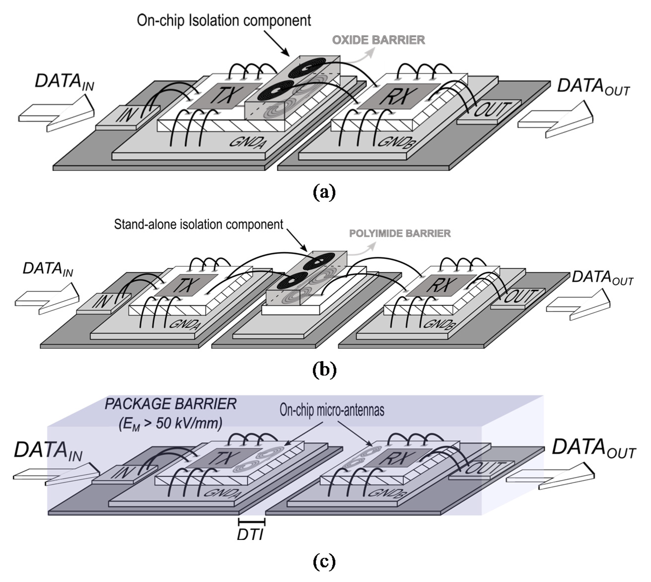
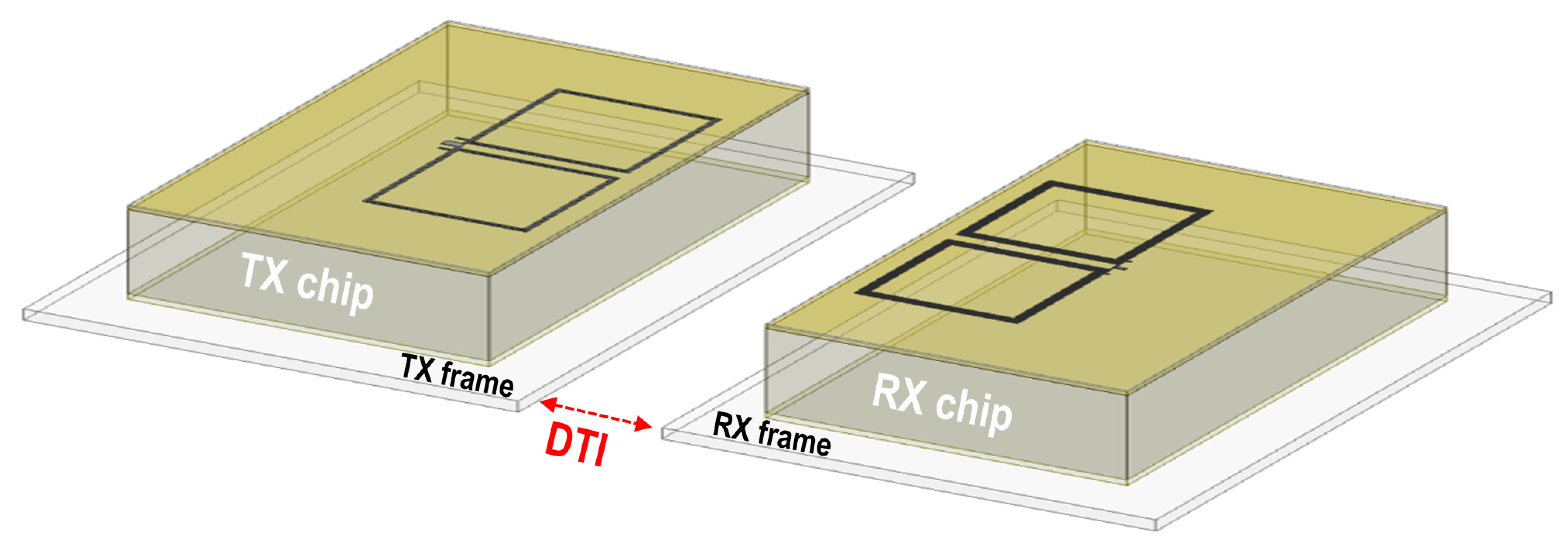
2.1. Chip-Scale Isolation vs. Package-Scale Isolation

The chip-scale isolation approach is based either on silicon dioxide (SiO2) or on polyimide layers, traditionally used in the semiconductor industry for intermetal isolation and wafer stress relief, respectively. Oxide and polyimide galvanic barriers have different breakdown voltage (BV), fabrication costs, and especially integration levels. Indeed, an oxide barrier can be integrated along with the active circuitry in a two-chip system-in-package (SiP) for each isolated channel (see Figure 2a), guaranteeing an isolation rating of about 6 kV thanks to the high SiO2 BV (i.e., about 1000 V/µm) [6,19]. However, oxide insulation is upper limited by the maximum reliable thickness (i.e., about 10 µm) due to both wafer mechanical stress and second-order BV effects. On the other hand, a polyimide layer can be used to build a stand-alone post-processed isolation-chip (i.e., a capacitor or a transformer) at the expense of a lower integration level (i.e., from two to three chips per each isolated channel, as shown in Figure 2b) [12,14]. Due to a lower BV (i.e., about 250 V/µm), a polyimide barrier requires about a three times thicker layer to sustain the same isolation voltage of an oxide barrier. The overall fabrication costs are the result of a complex combination of silicon and package costs, but typically a silicon-integrated isolation barrier is more expensive than a stand-alone post-processed polyamide one. In any case, both approaches are highly limited in terms of CMTI performance due to the relatively low distance trough insulator (DTI), which is in the order of tens of microns (typically from 10 μm to 30 μm). Indeed, due to such low DTI, the galvanic barrier exhibits high capacitive parasitics (in the order of tens of femtofarads), and hence high common-mode currents are produced by ground shifts, thus limiting the maximum tolerable voltage slope i.e., the CMTI performance.
Package-scale isolation drastically changes the traditional paradigm. Its key advantage is the use of the molding compound as an isolation layer between two side-by-side co-packaged chips along with the exploitation of a wider DTI (typically hundreds of microns between the chip lead frames) with the aim of increasing the isolation rating while reducing the capacitive parasitics of the galvanic barrier. The physical channel for data communication exploits the week near-field EM coupling (i.e., RF coupling) between two micro-antennas integrated on two side-by-side co-packaged chips, as shown in Figure 2c. In this approach, the DTI must be chosen to guarantee the required isolation rating, ensuring at the same time a reasonable coupling level between the micro-antennas. It should also be noted that the minimum value of the DTI can be often limited by packaging/assembling issues. Standard molding compounds exhibit dielectric strength (EM) of about 50–100 kV/mm, thus enabling reinforced isolation (i.e., VSURGE ≥ 10 kV) with a DTI of just 200 μm [20,21], which produces very low capacitive parasitics and hence CMTI better than 200 kV/μs [18].
Package-scale isolation based on RF coupling has other advantages compared to traditional isolation approaches. Firstly, a customized technology/component is not required, whereas standard packaging is sufficient to guarantee outstanding isolation and CMTI performance. Moreover, the approach is highly flexible and can be tailored to the application specifications without time-consuming and expensive technology development. On the other hand, such advantages are counterbalanced by a larger silicon area consumption due to on-chip antennas on both chips, as shown in Figure 2b. Finally, the RF coupling isolation approach is only suited to data transmission. In particular, due to high isolation channel loss, carrier-based modulation is mandatory to enable CMTI performance better than 200 kV/μs with a consequent higher power consumption compared to the impulsive modulation approaches. Package-scale isolation based on RF coupling is compared with the state-of-the-art approaches in Table 1.

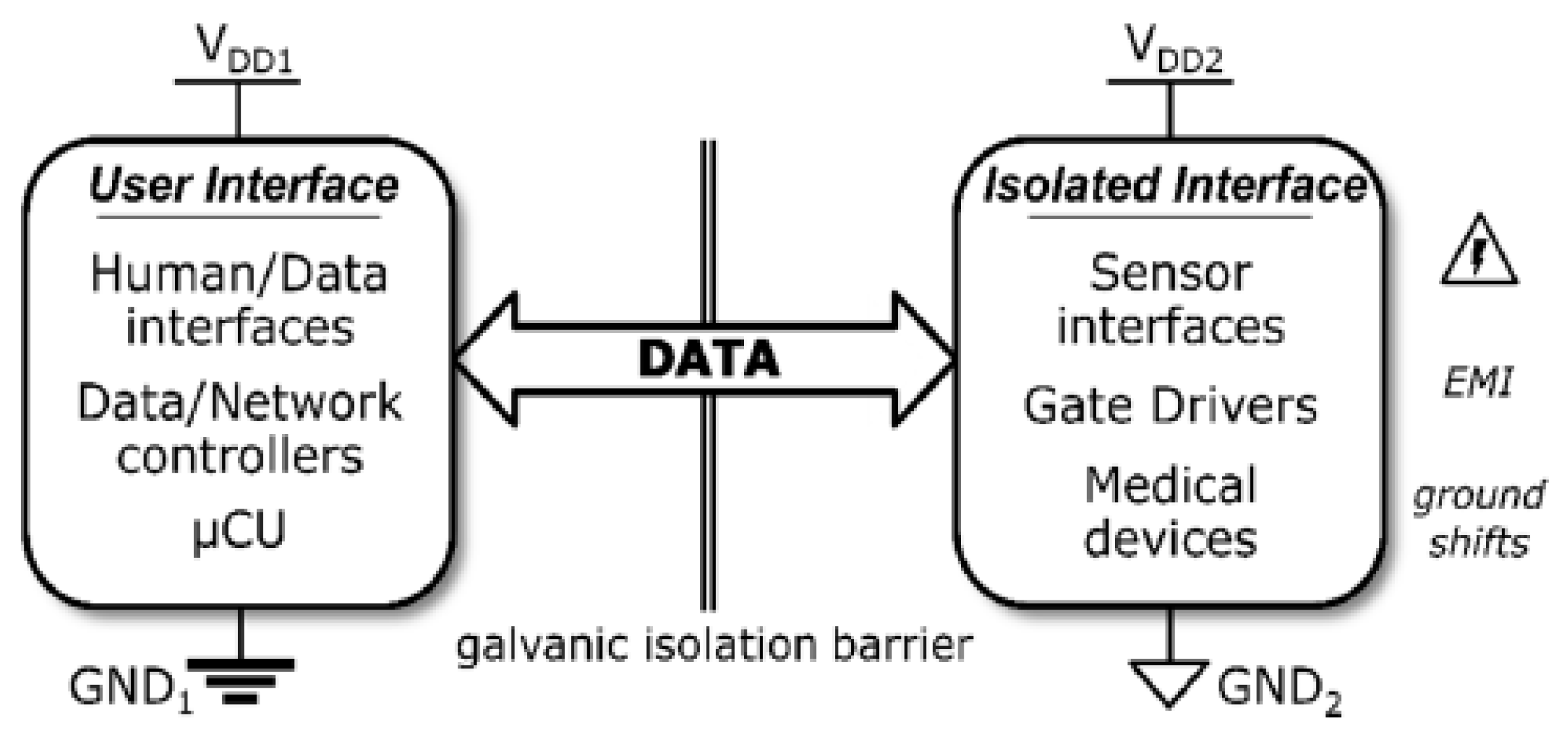
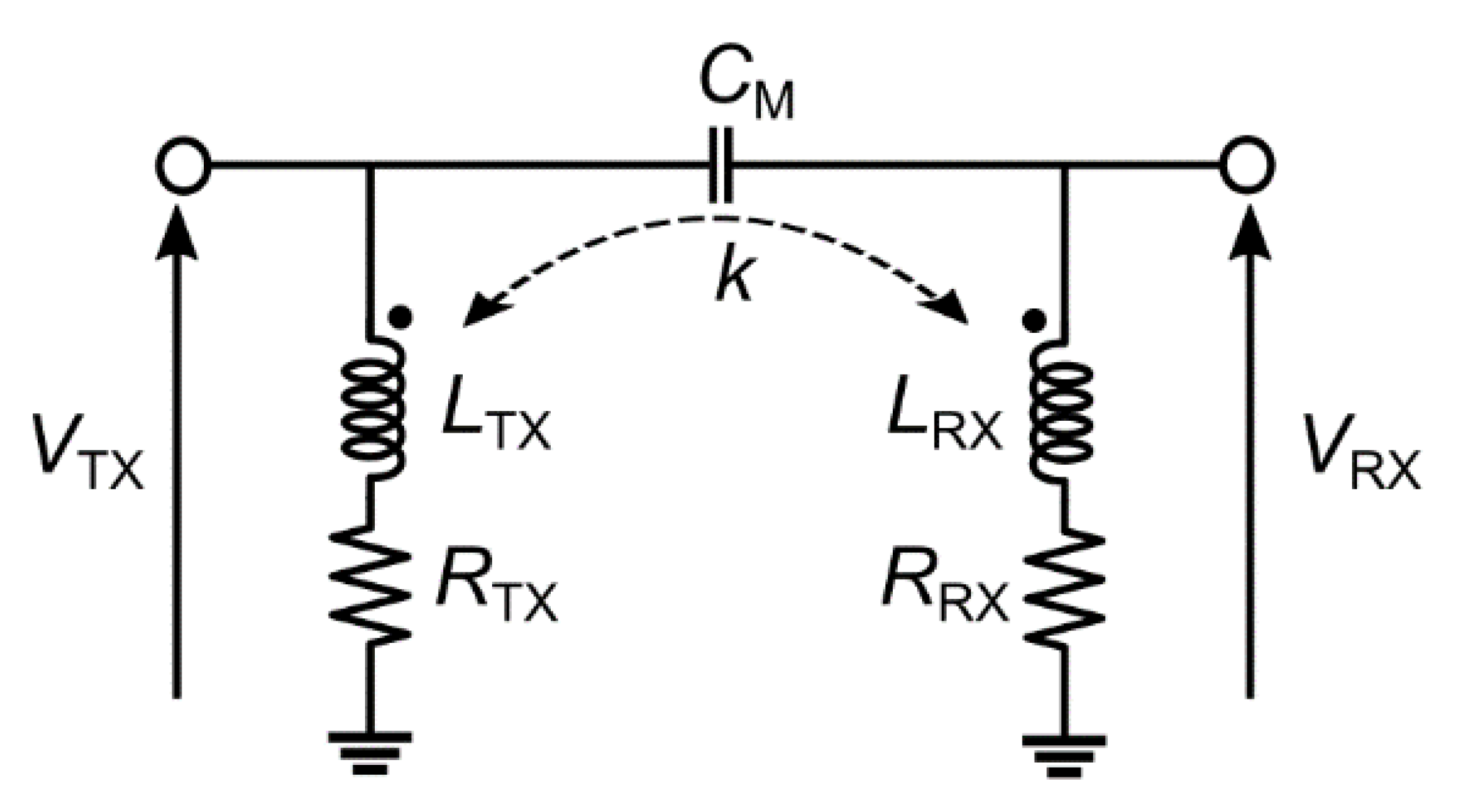
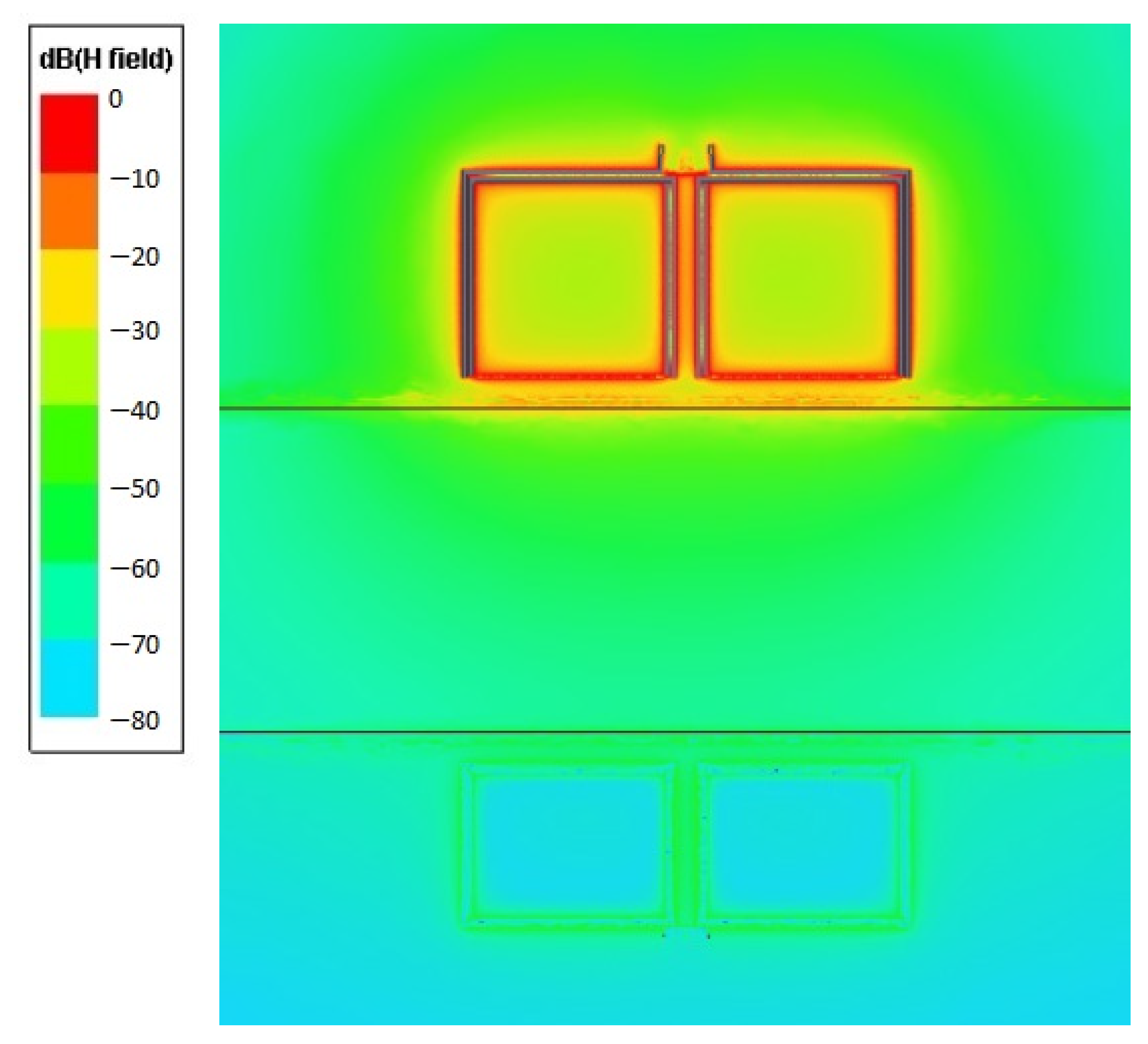
2.2. System Architecture and Circuit Description

The simplified block-diagram of a package-scale galvanic isolator based on RF planar coupling is shown in Figure 3 with reference to a single physical channel. Due to the extremely low magnetic coupling coefficient, k, between the transmitter (TX) and receiver (RX) micro-antennas, LTX, and LRX, carrier-based narrowband communication is mandatory to achieve significant performance in terms of both data rate and CMTI [16,17,18]. Typically, data transmission adopts on-off keying (OOK) pulse width modulation (PWM) of the RF carrier. Indeed, the PWM technique ensures higher robustness compared to the traditional amplitude-shift keying (ASK) modulation, since the bit information is the RF burst duration rather than its amplitude.
The TX front-end is integrated into Chip A and mainly consists of an RF oscillator adopting the micro-antenna, LTX, as an inductive tank. The oscillator is properly turned on and off by the PWM digital stream produced by the PWM modulator. Chip B integrates the RX front-end that exploits the RX micro-antenna, LRX, weakly coupled to the TX one, to detect the magnetically induced RF voltage. After rectifying and filtering, the RX envelope voltage, further amplified by the gain stage G, drives a hysteresis comparator to reconstruct the transmitted PWM signal. Finally, a baseband PWM demodulator is used to draw the original digital bit stream. Due to the high channel loss (about 30–45 dB depending on the adopted technology and chip distance), the system is operated in narrowband mode with both micro-antennas resonating at the RF carrier frequency, fRF.
The most critical blocks of the galvanic isolator architecture in Figure 3 are the RF oscillator and the rectifier stage. In particular, the RF oscillator design is very challenging due to stringent specifications in terms of the current consumption for a given oscillation voltage and the start-up time. When thick oxide/lateral transistors with high breakdown voltages are available, as in the BCD technologies [6,7,8,9,10], the D-class topology is highly preferred, as shown in Figure 4a. Indeed, the D-class oscillator boosts the oscillation voltage well above two times the supply voltage, VDD, [22] provided that the maximum drain-gate voltage VDG_MAX is high enough. Since the maximum allowable gate-source voltage, VGS_MAX, is smaller than VDG_MAX, coupling capacitors, CB, are used to perform a voltage partition with the gate capacitance of M1,2 thus properly setting the VGS peak to prevent gate-oxide breakdown. Additional capacitor CP is used to tune the oscillation frequency, fRF. Alternatively, if only standard MOS devices are available, the traditional inductor-loaded complementary cross-coupled oscillator shown in Figure 4b can be exploited. It maximizes the oscillation amplitude within the supply voltage, while giving the advantage of nearly doubled transconductance at the same current level compared with a simple cross-coupled oscillator, also minimizing the startup time. As far as the rectifier stage is concerned, key performance parameters are sensitivity and input impedance, along with CMTI and power consumption. A mixer-based solution has been adopted in [18]. However, it requires an additional pre-amplification stage and quite high-power consumption. On the other hand, very interesting solutions are based on common-source (CS) configurations that inherently provide high input impedance along with high gain, and lower power consumption, as in [23].
Typically, galvanically isolated interfaces require multi-channel capability, which can be implemented by multiplexing different data channels on the same physical link, provided that a sufficiently high data rate is available [11,14]. However, several applications also require bidirectional communication, such as in isolated gate drivers. For half-duplex data transfer, a single physical isolated link can be used, while full-duplex communication calls for an additional physical link [18] (see Figure 5).
The design of a bidirectional full-duplex galvanic isolator has to cope with the TX-to-RX cross-talk between channels, as represented in Figure 5. It can be fatal for data transmission due to the high loss of the isolated link. A simple solution is to increase the spacing between channels at the cost of a higher silicon area, as done in [18]. However, channel spacing must be more than twice the DTI to achieve a TX-to-RX rejection better than 15 dB. Therefore, it is mandatory to exploit different RF resonance frequencies (i.e., fRF separation) for each channel [16].

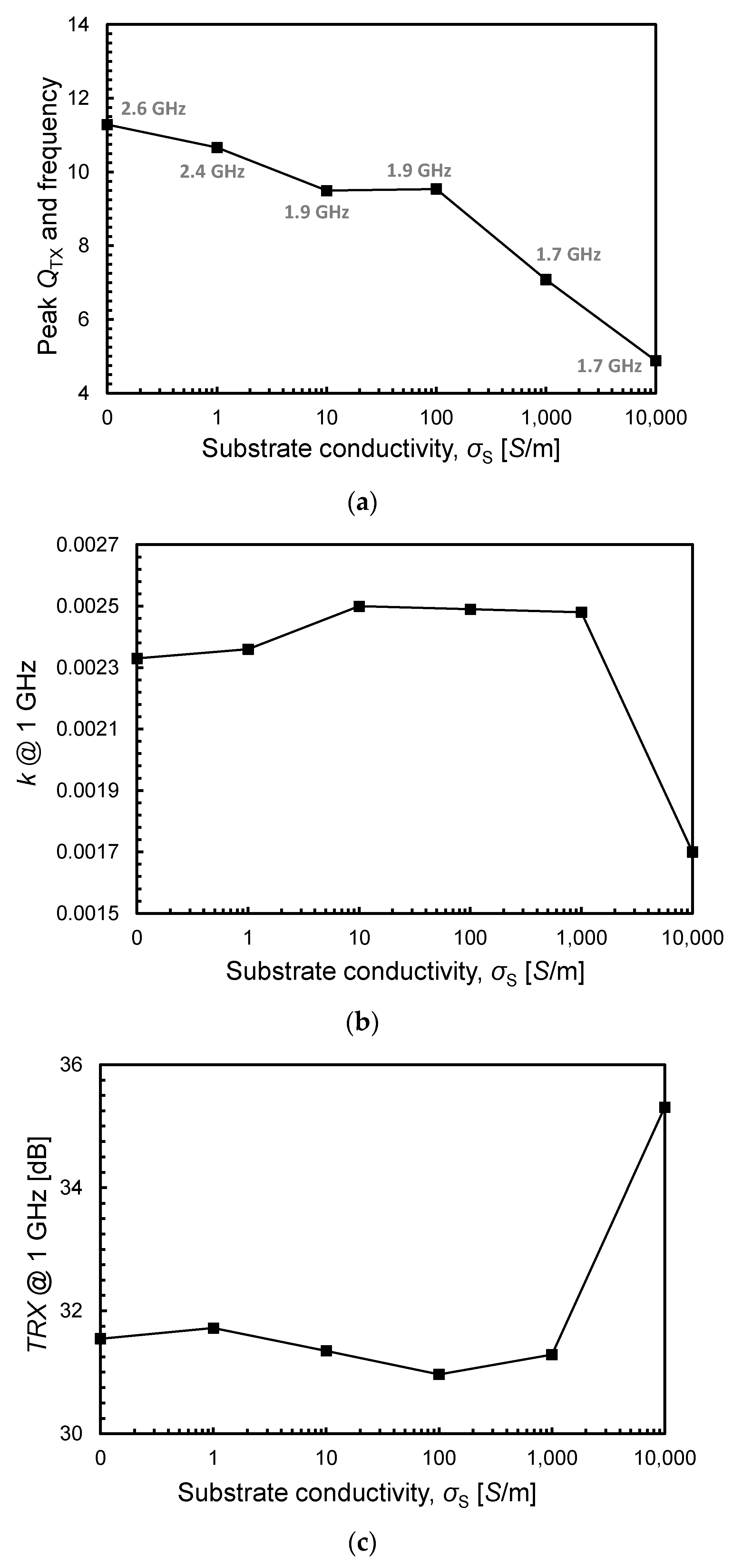
2.3. On-Chip Micro-Antenna Design Guidelines

The design of on-chip micro-antennas has several similarities with the design of RF spiral inductors [24]. However, in galvanic isolator applications, the main goal is the reduction of the channel loss that is highly related to antenna EM coupling. Therefore, some important differences with traditional inductors must be highlighted to properly address the micro-antenna design. As for inductive components, the integration process plays a key role since it determines the loss phenomena taking place in the substrate and the coil itself. Low conductivity substrate and thick top metal layers are crucial to reducing parallel and series losses, respectively. As far as the substrate conductivity, σS, is concerned, main performance parameters of micro-antennas are highly degraded for σS higher than 103 S/m, such as quality factors (QTX and QRX), magnetic coupling coefficient (k), and TX-to-RX coupling loss, as defined below [18].
T R X = 20 l o g 10 | V RX V TX |
where VRX and VTX are the voltage at the RX and TX micro-antennas, respectively.
This is demonstrated in Figure 6 by means of parametric 3D-EM simulations of a typical RX/TX antenna configuration at a distance of 600 μm. Specifically, reported curves reveal an optimum range of the substrate conductivity between 10 S/m and 100 S/m. Such conductivity values are typical for RF CMOS and BiCMOS technologies. Unfortunately, galvanic isolated interfaces are also required in standard BCD platforms, largely used in power applications (e.g., gate drivers). Such technologies adopt very highly doped substrate (σS > 104 S/m), which poses additional challenges in the micro-antenna design. In particular, the most representative performance parameter for galvanic isolators based on lateral RF coupling is the TX-to-RX coupling loss, TRX, in the resonance condition. As shown in Figure 6c, TRX is worsening by more than 4 dB for a substrate conductivity of 104 S/m. It is worth mentioning that for such isolators, it is mandatory that the system is operated in resonance condition to reduce the channel loss. This can be better understood by comparing the TRX performance with and without the resonance condition, which reveals an improvement of 13 dB at the operating frequency of 1 GHz, as depicted in Figure 7.
The main design target is minimizing the TX-to-RX coupling loss i.e., maximizing the induced voltage at the RX antenna for a given voltage at the TX one. A simple but effective design expression in open circuit condition can be easily drawn by modeling the isolated channel at the operative frequency, fRF, as shown in Figure 8. The adopted model takes into account the overall micro-antenna losses (i.e., both ohmic series losses and substate losses) by means of the equivalent resistances, RTX and RRX, series connected to the equivalent antenna inductance values, LTX, LRX. Magnetic and electric couplings between micro-antennas are modeled by the magnetic coupling factor, k, and parasitic capacitance, CM, respectively. In actual implementations, being a parasitic capacitor, CM, very low (i.e., below 5 fF), its coupling effect can be neglected to simplify calculations. The resulting design expression is reported below.
| V RX V TX | O C = k · N 1 + 1 Q TX 2
N = L RX L TX
From Equations (1)–(3), it is evident that minimizing TRX requires the maximization of the magnetic coupling coefficient, k, the step-up ratio, N, and quality factor of the TX antenna, QTX.
As far as the antenna shape is concerned, although polygonal and circular spirals achieve 10–20% higher Q-factors compared to squared ones at gigahertz frequencies [25,26], they do not ensure maximum EM coupling, thus recommending the use of square or rectangular coils, which benefit of longer laterally facing sides. The aspect ratio of the rectangular antenna, AR, (i.e., ratio of its longer-facing side to its shorter side) must be optimized by accounting for contrasting performance, such as the Q-factor and the EM coupling (see Figure 9). Indeed, the higher is AR the lower is the coil Q-factor, due to increased current crowding into the inner windings [27], the higher is the EM coupling between antennas thanks to longer-facing sides. Moreover, if bidirectional channels are present, the TX-to-RX cross-talk plays an important role in defining the antenna AR. Indeed, exploiting an AR higher than one also reduces the parasitic EM coupling between different adjacent channels (see Figure 5).
A final consideration is about the TX antenna spiral layout, which has to comply with the adopted oscillator topology. Indeed, a simple not symmetric spiral can be used in a complementary cross-coupled oscillator (see Figure 4b), as in [16,18]. On the other hand, if a D-class oscillator is preferred, a symmetric antenna topology is mandatory to ensure the central tap connection for the supply voltage, VDD. In this situation, an effective solution to increase the EM coupling between antennas is the adoption of two identical coils in a U-shape fashion, as shown in Figure 10, since the current flowing in the antenna has a clock-wise direction in both single windings.
The starting point for the design of the micro-antennas is the definition of their layout parameters (i.e., the number of turns, n, the inner diameter, dIN, the metal width, w, and the metal spacing, s) to set the low-frequency inductance values. The latter can be easily calculated with good precision by means of closed-form equations available in the literature [28], also enriched with the metal thickness, t, to improve the accuracy for high t/w ratio (i.e., very thick and/or narrow coils). The antenna inductance, LRX, is mainly dependent on the number of turns, n, and the inner diameter, dIN. Given the operative frequency, fRF, LRX is also upper bounded by the input parasitic capacitance of the RX front-end. A general design guideline is using a small metal width, w, along with a high number of turns to achieve the highest value of the inductance-to-area ratio and therefore the highest self-resonance frequency for the RX antenna. It is worth mentioning that if the input impedance of the RX front-end (i.e., of the envelope detector in Figure 3) is sufficiently high (i.e., nearly open condition), the degradation of the QRX due to a small w is irrelevant for the induced voltage at the RX antenna. Given the LRX value, the maximization of the step-up ratio, N, calls for the use of the lowest value of LTX (i.e., low number of turns) compatible with a proper operation of the RF oscillator in terms of startup time and power consumption. In this perspective, since a crucial role is played by the ωQL product of the TX antenna, the maximization of the Q-factor is mandatory. To this aim, a sufficiently large metal width, w, is preferable, while the coil external diameter is already defined by the RX antenna geometry to maximize the TX-to-RX EM coupling.
A final consideration has to be done about the tuning between the TX oscillation frequency, fRF, and the RX antenna resonance frequency, fRX, which is mandatory to minimize TRX, as shown in Figure 7. On the TX side, since the oscillator core parasitic capacitances are highly nonlinear due to signal variations of several volts, they are very difficult to be accurately modeled [29]. To avoid unpredictable simulation errors, it is highly suggested to set the oscillation frequency, fRF, by means of a dominant parallel capacitor CP (i.e., at least ten times higher than the parasitic capacitance) and then consider its statistical variations within a Montecarlo simulation run. On the RX side, small-signal modeling of the envelope detector parasitic capacitances is sufficiently reliable, but an additional small capacitance can be used for fine-tuning of fRX.

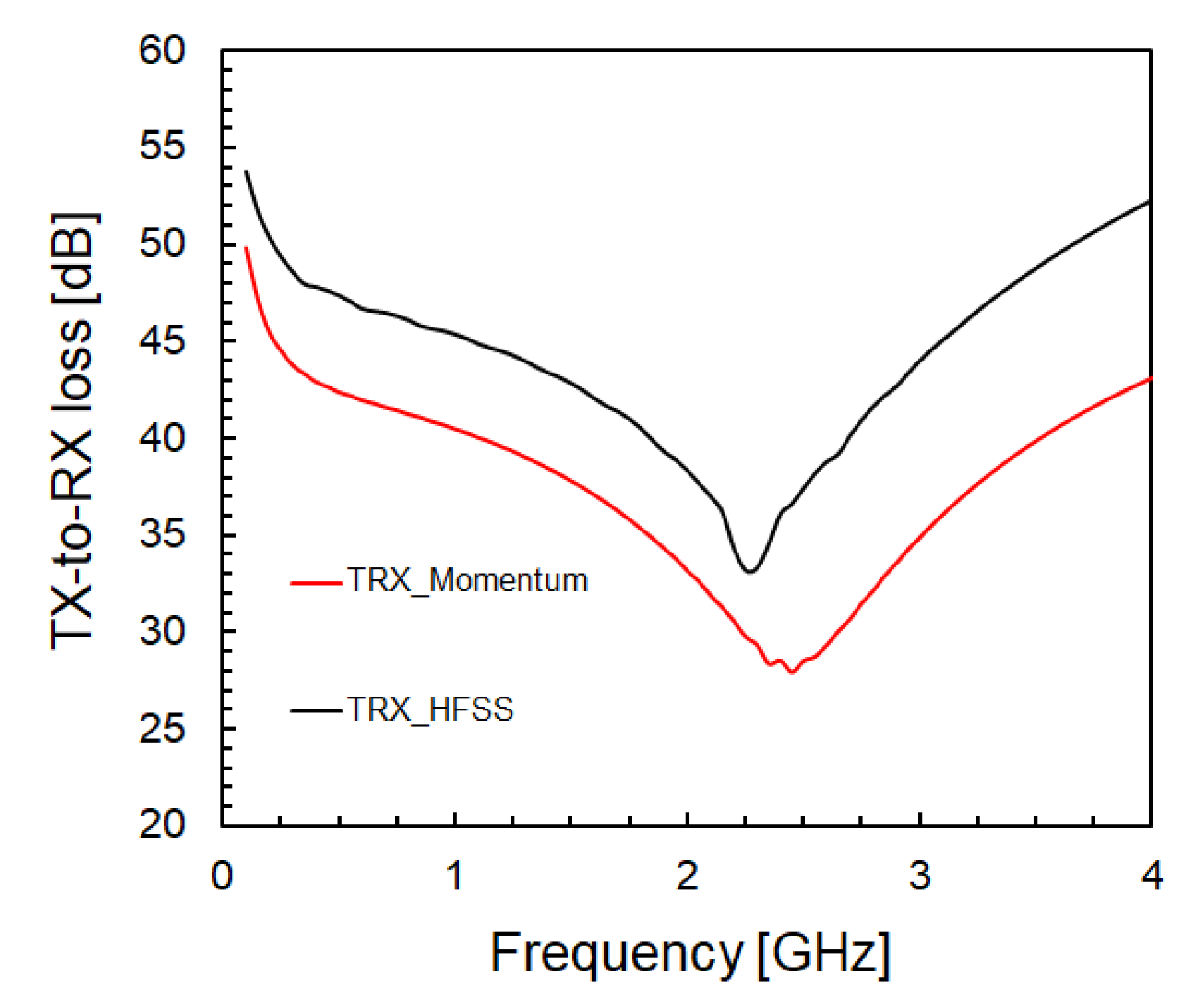
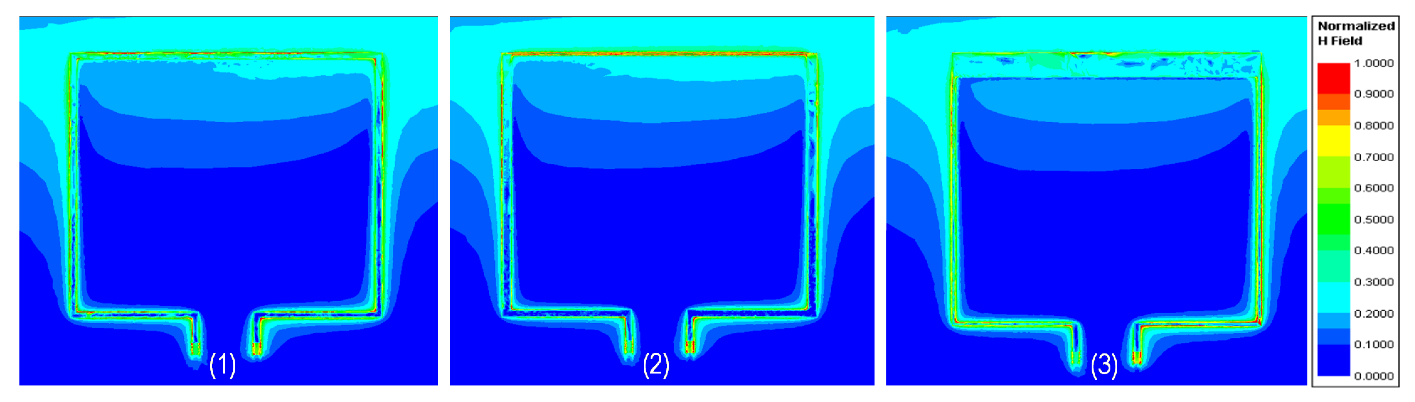
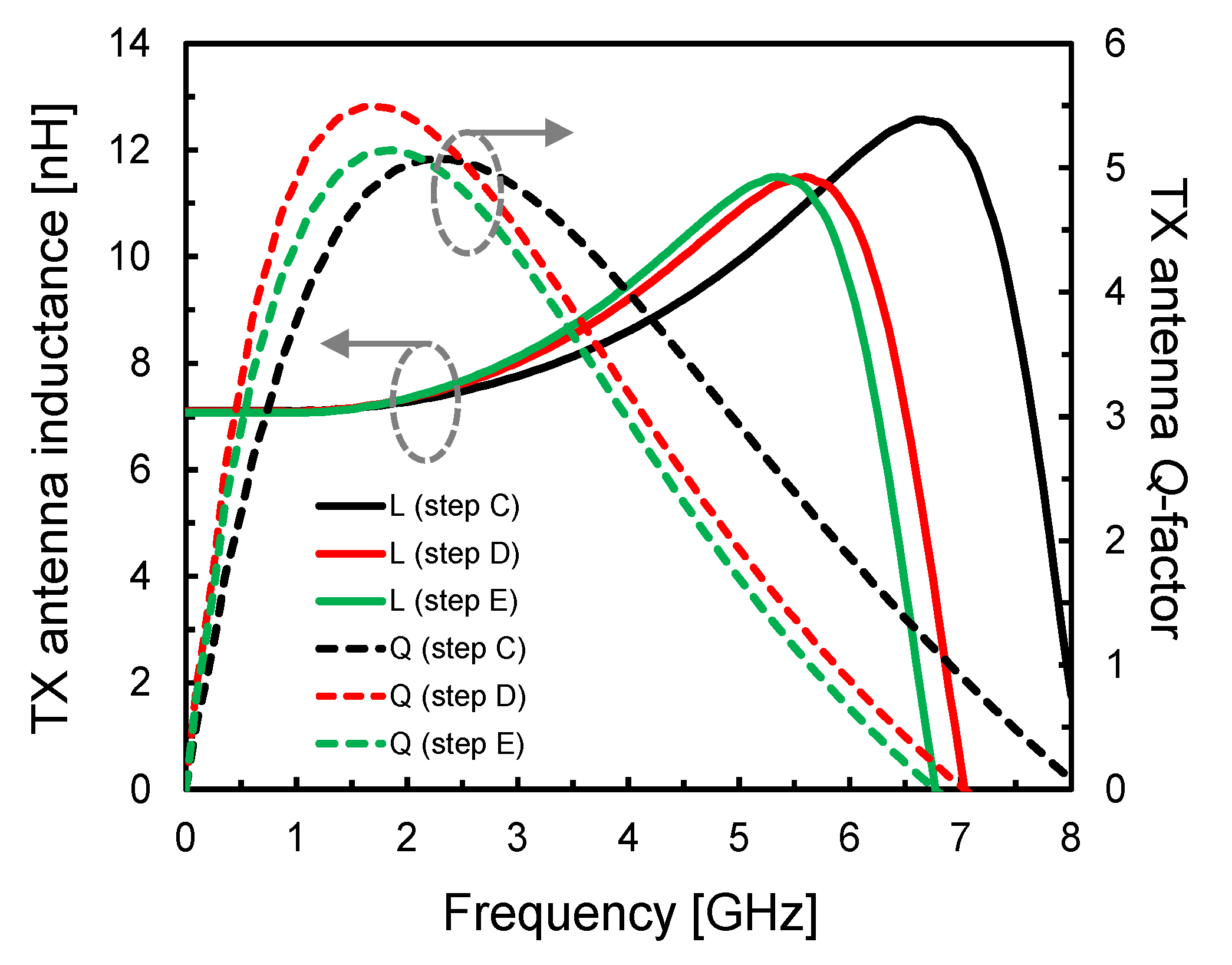
3. Micro-Antenna Optimization

3.1. On-Chip Micro-Antenna Design Guidelines

In this work, a 0.32-μm BCD technology by STMicroelectronics has been used for each of the two side-by-side co-packaged chips. The process provides a BEOL with three thin Al layers along with a top thick Cu metal. This fabrication technology had been chosen since it is largely adopted in high-voltage applications (i.e., for gate drivers in both industrial and automotive environments). Moreover, it offers high-voltage, laterally diffused metal-oxide-semiconductor (LDMOS) transistors well suited to implement a D-class oscillator. However, it adopts a very conductive silicon substrate (i.e., σS is about 104 S/m) which is very critical for the EM coupling between the micro-antennas (see Figure 6). The adoption of such technology for a package-scale galvanic isolator, is particularly useful to highlight some design issues. Indeed, the high value of σS requires careful optimization of the micro-antennas to minimize the TX-to-RX coupling loss. The design of the galvanic isolator has been carried out by means of EM simulations of the micro-antennas. Although time-consuming, a 3D full-wave simulator (i.e., Ansoft HFSS) was preferred to a more traditional 2D (i.e., Keysight ADS Momentum) one due to its higher accuracy in terms of EM coupling when the substrate conductivity is quite high. In this regard, Figure 11 reports a comparison between the results obtained by the two mentioned EM tools for the same antenna configuration. The average error in terms of TRX is about 6 dB in the analyzed frequency range, which is probably due to the parasitic couplings through the highly conductive substrate that a 2D simulator is not able to distinguish for each antenna dice.
A 3D-view of the simulated antennas in HFSS is shown in Figure 12. For the EM simulation set-up, a box of molding compound surrounding the two chips was encased within a box of air. A first-order absorbing boundary condition (ABC) was assigned on the whole air-box surface except for the two regions under the chip frames where perfect-E boundary conditions hold. Each micro-antenna was excited by means of three lumped ports (i.e., the two-terminal and the center tap connection). Finite tetrahedral first-order elements were used for the mesh, which was adaptively refined through ten steps. Moreover, in order to improve the solution quality, an additional mesh refinement was adopted in the antenna metal traces and in the molding compound region between the dies. Finally, the solution frequency was equal to the operative frequency, fRF, while a wider frequency sweep from 0.1 GHz up to 8 GHz was set.

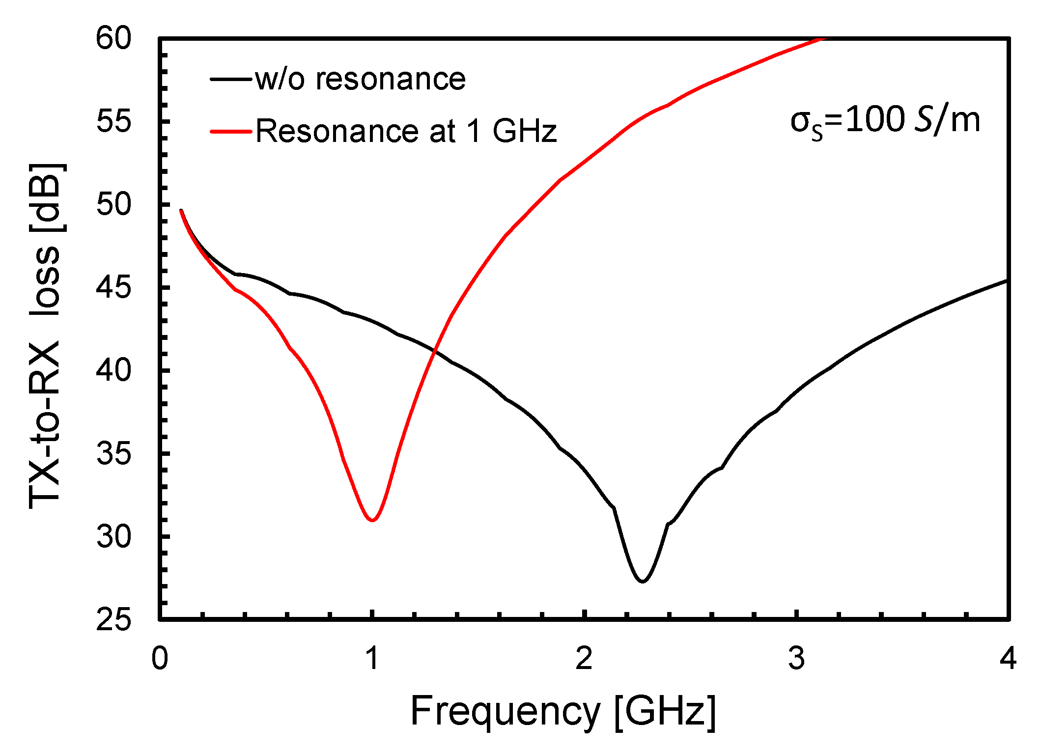
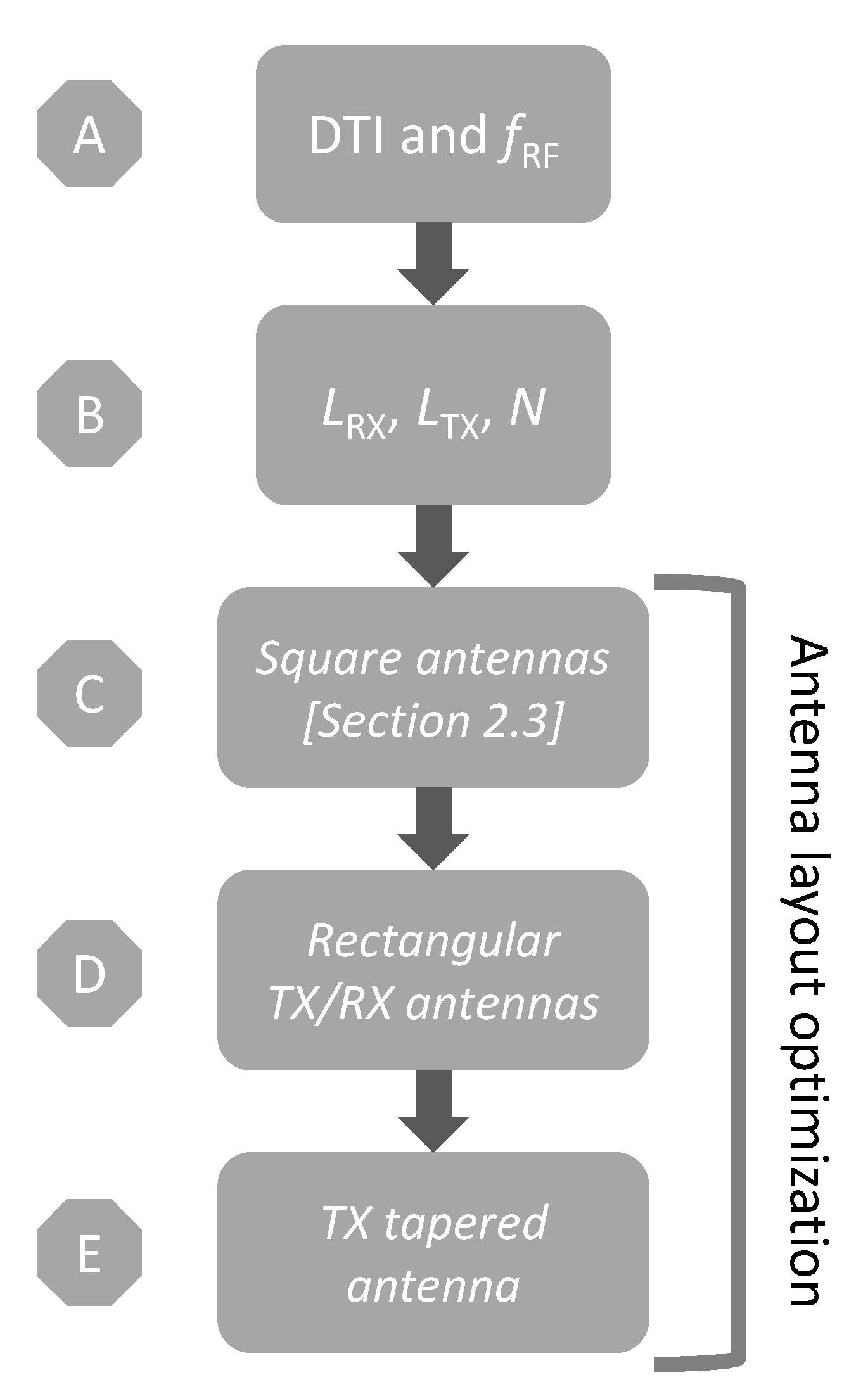
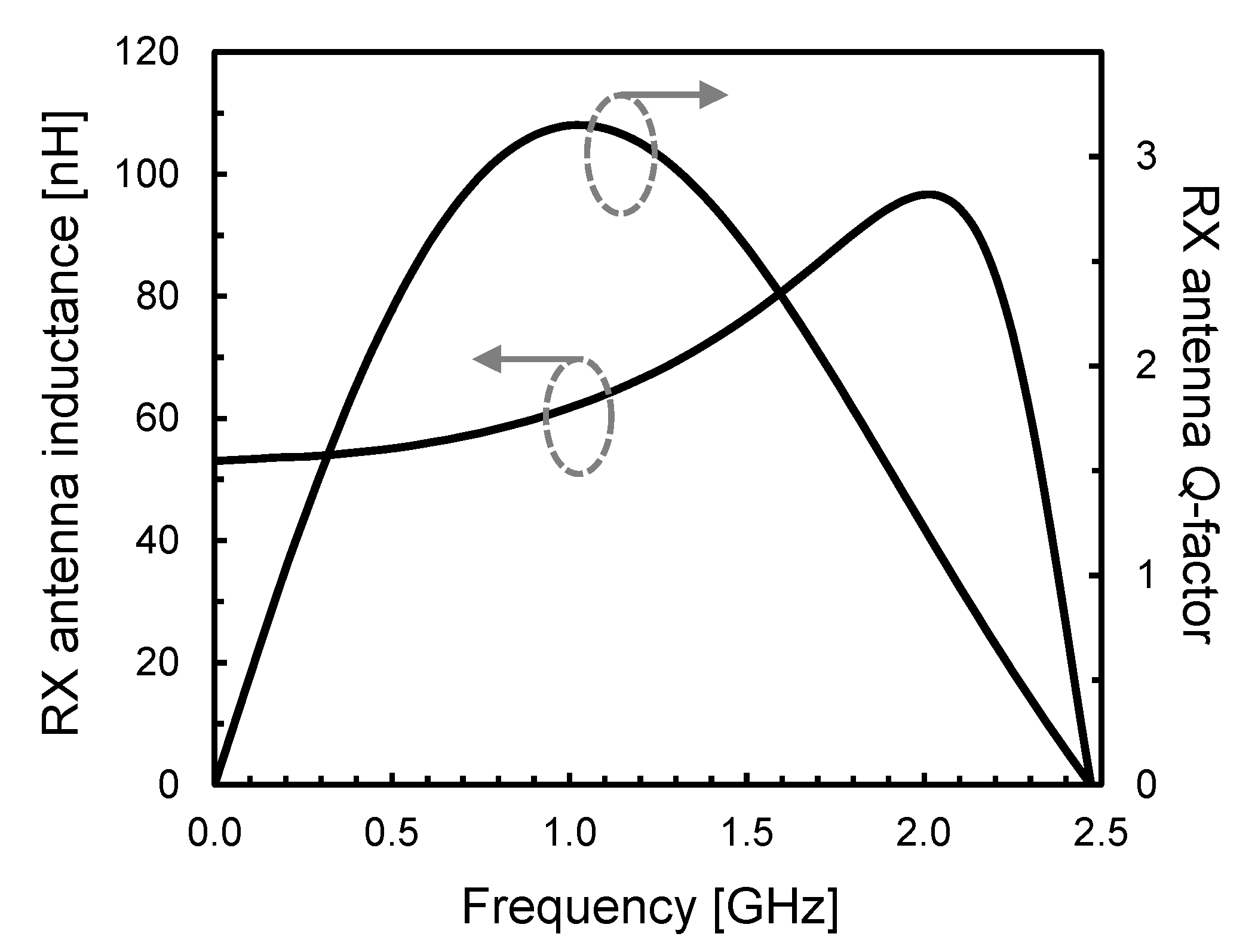
3.2. Optimization Flow for TX and RX Antennas

The adopted design flow is described in the block diagram in Figure 13. The first step, A, includes the definition of the DTI between chips and RF carrier frequency, fRF. The DTI must comply with both the isolation rating and assembling constraints. In this design example, it has been set to 500 μm to achieve an isolation rating higher than 10 kV (i.e., reinforced isolation) by using a standard molding compound (εr = 5.5). The RF carrier frequency, fRF, is upper limited by the oscillator operation at a given current budget. Other constraints could be related to the specific application (i.e., data rate, channel multiplexing, EM emissions or external interferences, etc.). In this work, fRF has been set equal to 1.5 GHz.
In step B, both antenna inductance values are properly chosen. The starting point is the RX antenna inductance, LRX, which is set to the highest possible value compatible with the input capacitance of the RX front-end. The voltage step-up ratio, N, is then maximized by using the lowest value of the TX antenna inductance, LTX, that allows the RF oscillator to be properly operated at a reasonable value of QTX and without exciding the current consumption constraint.
As previously said, the design of the micro-antenna layout is crucial to minimize the TX-to-RX coupling loss. Indeed, according to (2) and (3), the maximization of the magnetic coupling coefficient, k, must be pursued. In the flow diagram shown in Figure 13, a three-step optimization is proposed for the antenna geometry optimization (namely steps C, D, and E). Table 2 summarizes the main antenna geometrical parameters for each layout configuration. It is worth noting that through the whole optimization process both LTX and LRX and thus N, are kept broadly constant at the operative frequency (about 7 nH and 78 nH for LTX and LRX, respectively). In the initial antenna optimization step (C in Figure 13), both TX/RX coils have been drawn according to the general design guidelines discussed in Section 2. Specifically, square antennas with two windings in a U-shape fashion have been designed, as shown in Figure 10 and Figure 12. For the RX antenna, the minimum allowed metal trace (i.e., 1.6 µm) has been chosen. On the other hand, the width of the TX spiral has been properly set to comply with the minimum Q-factor, QTX_MIN, required by the RF oscillator. It is worth noting that in the adopted BCD technology the antenna Q-factors are very low due to highly conductive substrate, which produces a consequent increase of the oscillator current consumption. Specifically, using a D-class oscillator topology with LDMOS devices, the minimum value of the Q-factor for the TX antenna, QTX_MIN, is equal to 4 in the adopted process for a TX current budget of about 15 mA.
Moving to the next optimization step (D in Figure 13), the rectangular shape is adopted for both antennas. The aim is to exploit longer laterally facing sides of the antennas to improve the magnetic coupling, as claimed in (2). The aspect ratio, AR, of the RX antenna has been increased up to 1.3, still ensuring almost the same self-resonance frequency, SRF. On the other hand, for the TX antenna, only a slight variation of AR is allowed in order to avoid a further Q-factor degradation due to the increase of inner coil current crowding effects. It is worth mentioning that the TX coil perimeter increases going from step C to step D, thus allowing an effective increase of the metal width (from 4 to 7 µm) to keep the LTX value almost constant.
In the last step E, further optimization is carried out by using a tapered coil configuration (i.e., using a variable width in the same coil) with the aim of increasing the magnetic coupling between the RF micro-antennas. To properly drive the design of an effective tapered coil, three simple test cases for package-scale RF isolators have been compared by means of 3D EM simulations. Each adopted test case employs two identical one-turn square coils for both RX and TX antennas, respectively, whose main geometrical and electrical parameters are summarized in Table 3.
The operative frequency has been chosen about a fifth of the SRF since a similar proportion holds for the TX antenna in the actual isolator design. Specifically, the first test case is the reference one since it adopts a traditional single turn coil with a fixed width (i.e., 8 µm). Two different tapered structures are evaluated, which are obtained by using a reduced or enlarged width for the antenna facing side for test cases 2 and 3, respectively (i.e., 2 or 32 µm). To keep constant both inductance and, to some extent, the SRF, the width of the non-facing sides is properly increased or reduced for test cases 2 and 3, respectively.
Figure 14 compares the magnetic field distribution for the simulated test cases. EM simulations reveal that the magnetic field strength in the antenna facing side becomes greater as the width decreases. On the other hand, the magnetic field in the non-facing sides reduces as the width increases. This qualitative analysis is further confirmed by the magnetic coupling coefficient, k, that achieves the highest value for test case 2, as shown in Table 2. However, in the actual isolator design, the trace width of the RX antenna has been already minimized (i.e., the slightest width allowed by the technology) and no further improvements are achieved by a tapered structure that instead can be adopted for the TX antenna, as detailed in Table 2.
Figure 15 reports both inductance and Q-factor curves of the TX antenna for each design steps C, D, and E. On the other hand, no significant performance variations occur in the RX antenna from design step C (see Figure 16) to D, while the antenna remains unchanged from D to E. The increase of the TX antenna parasitic capacitance produces a slight reduction of its SRF, while the Q-factor at the operating frequency of 1.5 GHz always guarantees a proper operation of the RF oscillator (i.e., higher than QTX_MIN). Thanks to the antenna optimization procedure, the magnetic coupling factor, k, is improved by about 19% from steps C to E, which, in turn, produces a reduction of the TX-to-RX coupling loss in open circuit and resonance condition of about 1.7 dB, as shown in Figure 17.
For the sake of completeness, Figure 18 depicts the magnetic field distribution at the operative frequency (i.e., 1.5 GHz) for the TX/RX micro-antenna configuration in design step E, obtained by means of 3D EM simulations with a TX antenna differential excitation.

4. Conclusions

This paper has disclosed an effective design procedure of on-chip micro-antennas for package-scale galvanic isolators based on RF planar coupling. For the first time, key design guidelines have been proposed and then the antenna optimization flow has been verified by means of 3D EM simulations carried out for a galvanic isolator integrated in a 0.32-μm BCD technology. The main results of the proposed optimization procedure are:
(1)
a significant improvement of the EM coupling in terms of magnetic coupling factor (i.e., 19% in the reported design example)
(2)
a consequent reduction of the TX-RX coupling loss (i.e., 1.7 dB in the reported design example).
Such performance has been achieved without affecting the design parameters related to both TX and RX front-ends, being only the result of the optimization of the galvanically isolated channel. The proposed micro-antenna design procedure will be adopted in the next integrations of complete package-scale galvanic isolators in different technology platforms (i.e., CMOD. BCD, GaN).

Author Contributions

Conceptualization E.R.; validation S.S. and E.R.; formal analysis S.S. and E.R.; investigation, S.S., N.S. and E.R.; project administration, E.R.; supervision, E.R.; writing—original draft, E.R.; writing—review and editing, E.R. All authors have read and agreed to the published version of the manuscript.

Funding

This work was supported in part by the University of Catania through the Project “Programma Ricerca di Ateneo UNICT 2020-22 linea 2”.

Data Availability Statement

The data presented in this study are available on request from the corresponding author.

Conflicts of Interest

The authors declare no conflict of interest.

References

  1. DIN VDE Semiconductor Devices-Magnetic and Capacitive Coupler for Basic and Reinforced Isolation, VDE Verlag VDE V 0884-11. January 2017. Available online: https://www.vde-verlag.de/standards/0800375/dinvde-v-0884-11-vde-v-0884-11-2017-01.html (accessed on 8 December 2021).
  2. Kazanbas, M.; Schittler, A.; Araújo, S.; Zacharias, P. High-Side Driving under High-Switching Speed: Technical Challenges and Testing Methods. In Proceedings of the PCIM Europe 2015; International Exhibition and Conference for Power Electronics, Intelligent Motion, Renewable Energy and Energy Management, Nuremberg, Germany, 19–20 May 2015. [Google Scholar]
  3. Ragonese, E.; Palmisano, G.; Parisi, A.; Spina, N. Highly Integrated Galvanically Isolated Systems for Data/Power Transfer. In Proceedings of the 2019 26th IEEE International Conference on Electronics, Circuits and Systems, ICECS 2019, Genoa, Italy, 27–29 November 2019; pp. 518–521. [Google Scholar]
  4. Shi, G.; Yan, R.; Xi, J.; He, L.; Ding, W.; Pan, W.; Liu, Z.; Yang, F.; Chen, D. A Compact 6 Ns Propagation Delay 200 Mbps 100 KV/μs CMR Capacitively Coupled Direction Configurable 4-Channel Digital Isolator in Standard CMOS. In Proceedings of the 2018 25th IEEE International Conference on Electronics Circuits and Systems, ICECS 2018, Bordeaux, France, 9–12 December 2018; pp. 721–724. [Google Scholar]
  5. Texas Instruments. ISO7841x High-Performance, 8000-VPK Reinforced Quad-Channel Digital Isolator. Available online: http://www.ti.com (accessed on 8 December 2021).
  6. Fiore, V.; Ragonese, E.; Palmisano, G. A Fully Integrated Watt-Level Power Transfer System with On-Chip Galvanic Isolation in Silicon Technology. IEEE Trans. Power Electron. 2017, 32, 1984–1995. [Google Scholar] [CrossRef]
  7. Ragonese, E.; Spina, N.; Castorina, A.; Lombardo, P.; Greco, N.; Parisi, A.; Palmisano, G. A Fully Integrated Galvanically Isolated DC-DC Converter with Data Communication. IEEE Trans. Circuits Syst. I Regul. Pap. 2018, 65, 1432–1441. [Google Scholar] [CrossRef]
  8. Erlbacher, T. Lateral Power Transistors in Integrated Circuits; Power Systems; Springer: Cham, Switzerland, 2014. [Google Scholar]
  9. Moscatelli, A.; Merlini, A.; Croce, G.; Galbiati, P.; Contiero, C. LDMOS Implementation in a 0.35 Μm BCD Technology (BCD6). In Proceedings of the IEEE International Symposium on Power Semiconductor Devices and ICs (ISPSD), Toulouse, France, 22–25 May 2000; pp. 323–326. [Google Scholar]
  10. Riccardi, D.; Causio, A.; Filippi, I.; Paleari, A.; Pregnolato, L.V.A.; Galbiati, P.; Contiero, C. BCD8 from 7V to 70V: A New 0.18μm Technology Platform to Address the Evolution of Applications towards Smart Power ICs with High Logic Contents. In Proceedings of the International Symposium on Power Semiconductor Devices and ICs, Jeju, Island, 27–31 May 2007; pp. 73–76. [Google Scholar]
  11. Parisi, A.; Ragonese, E.; Spina, N.; Palmisano, G. Galvanically Isolated DC-DC Converter Using a Single Isolation Transformer for Multi-Channel Communication. IEEE Trans. Circuits Syst. I Regul. Pap. 2020, 67, 4434–4444. [Google Scholar] [CrossRef]
  12. Chen, B. iCoupler® Products with isoPower™ Technology: Signal and Power Transfer across Isolation Barrier Using Microtransformers. Technical Article, Analog Devices, USA. Available online: http://www.analog.com/media/cn/technical-documentation/technical-articles/isoPower.pdf?doc=CN0185.pdf (accessed on 8 December 2021).
  13. Qin, W.; Yang, X.; Ma, S.; Liu, F.; Zhao, Y.; Zhao, T.; Chen, B. 15.5 An 800 mW Fully Integrated Galvanic Isolated Power Transfer System Meeting CISPR 22 Class-B Emission Levels with 6 dB Margin. In Proceedings of the Digest of Technical Papers—IEEE International Solid-State Circuits Conference, San Francisco, CA, USA, 17–21 February 2019; pp. 246–248. [Google Scholar]
  14. Tan, Z.; Mueck, M.; Du, X.H.; Getzin, L.; Guidry, M.; Keating, S.; Xing, X.; Zhao, F.; Chen, B. A Fully Isolated Delta-Sigma ADC for Shunt Based Current Sensing. IEEE J. Solid-State Circuits 2016, 51, 2232–2240. [Google Scholar] [CrossRef]
  15. Greco, N.; Parisi, A.; Lombardo, P.; Spina, N.; Ragonese, E.; Palmisano, G. A Double-Isolated DC-DC Converter Based on Integrated LC Resonant Barriers. IEEE Trans. Circuits Syst. I Regul. Pap. 2018, 65, 4423–4433. [Google Scholar] [CrossRef]
  16. Mukherjee, S.; Bhat, A.N.; Shrivastava, K.A.; Bonu, M.; Sutton, B.; Gopinathan, V.; Thiagarajan, G.; Patki, A.; Malakar, J.; Krishnapura, N. A 500 Mb/s 200 pJ/b Die-to-Die Bidirectional Link with 24 kV Surge Isolation and 50 kV/Μs CMR Using Resonant Inductive Coupling in 0.18 µm CMOS. In Proceedings of the Digest of Technical Papers—IEEE International Solid-State Circuits Conference, San Francisco, CA, USA, 5–9 February 2017; Volume 60, pp. 434–435. [Google Scholar]
  17. Ragonese, E.; Spina, N.; Parisi, A.; Palmisano, G. Reinforced Galvanic Isolation: Integrated Approaches to Go Beyond 20-kV Surge Voltage (invited). In Applications in Electronics Pervading Industry, Environment and Society; Saponara, S., De Gloria, A., Eds.; ApplePies 2019. Lecture Notes in Electrical Engineering; Springer: Cham, Switzerland, 2020; Volume 627, pp. 277–283. [Google Scholar]
  18. Ragonese, E.; Spina, N.; Parisi, A.; Palmisano, G. A Cmos Data Transfer System Based on Planar RF Coupling for Reinforced Galvanic Isolation with 25-Kv Surge Voltage and 250-Kv/Μs CMTI. Electronics 2020, 9, 943. [Google Scholar] [CrossRef]
  19. Mahalingam, P.; Guiling, D.; Lee, S. Manufacturing Challenges and Method of Fabrication of On-Chip Capacitive Digital Isolators. In Proceedings of the 2007 International Symposium on Semiconductor Manufacturing, Santa Clara, CA, USA, 15–17 October 2007; pp. 1–4. [Google Scholar]
  20. Paye, J.; Claudi, A.; Stecher, M. High Voltage Robustness of Mold Compounds under Different Environmental Conditions. In Proceedings of the IEEE International Reliability Physics Symposium Proceedings, Monterey, CA, USA, 19–23 April 2015; pp. CP51–CP56. [Google Scholar]
  21. Paye, J.; Claudi, A.; Stecher, M. High Voltage Robustness of Mold Compounds after Different Treatments. In Proceedings of the 34th Electrical Insulation Conference, EIC 2016, Montreal, QC, Canada, 19–22 June 2016; pp. 162–165. [Google Scholar]
  22. Fanori, L.; Andreani, P. Class-D CMOS Oscillators. IEEE J. Solid-State Circuits 2013, 48, 3105–3119. [Google Scholar] [CrossRef]
  23. Fiore, V.; Ragonese, E.; Palmisano, G. Low-Power ASK Detector for Low Modulation Indexes and Rail-to-Rail Input Range. IEEE Trans. Circuits Syst. II Express Briefs 2016, 63, 458–462. [Google Scholar] [CrossRef]
  24. Spataro, S.; Ragonese, E. Design and Optimization of Silicon-Integrated Inductive Components for Automotive Radar Applications in k-and w-Bands. In Proceedings of the 2020 AEIT International Conference of Electrical and Electronic Technologies for Automotive, AEIT AUTOMOTIVE 2020, Turin, Italy, 18–20 November 2020. [Google Scholar]
  25. Chaki, S.; Aono, S.; Andoh, N.; Sasaki, Y.; Tanino, N.; Ishihara, O. Experimental Study on Spiral Inductors. In Proceedings of the 1995 IEEE MTT-S International Microwave Symposium, Orlando, FL, USA, 16–20 May 1995; Volume 2, pp. 753–756. [Google Scholar]
  26. Mohan, S.S. The Design, Modeling and Optimization of on Chip Inductor and Transformer Circuit. Ph.D. Thesis, Department of Electrical Engineering, Stanford University, Stanford, CA, USA, 1999. [Google Scholar]
  27. Craninckx, J.; Steyaert, M.S.J. A 1.8-GHz Low-Phase-Noise CMOS VCO Using Optimized Hollow Spiral Inductors. IEEE J. Solid-State Circuits 1997, 32, 736–744. [Google Scholar] [CrossRef] [Green Version]
  28. Mohan, S.S.; Hershenson, M.D.M.; Boyd, S.P.; Lee, T.H. Simple Accurate Expressions for Planar Spiral Inductances. IEEE J. Solid-State Circuits 1999, 34, 1419–1420. [Google Scholar] [CrossRef] [Green Version]
  29. McAndrew, C.C.; Lorenzo-Cassagnes, A.; Goyhenetche, P.; Pigott, J.; Yao, W.; Gildenblat, G.; Victory, J. Advances in LDMOS Compact Modeling for IC Design: The SP-HV Model and Its Capabilities. IEEE Solid-State Circuits Mag. 2014, 6, 35–46. [Google Scholar] [CrossRef]
Figure 1. Simplified block diagram of a galvanically isolated system.
Electronics 11 00291 g001
Figure 2. Chip-scale versus package-scale isolation: integrated barrier (a); stand-alone post-processed barrier (b); package-scale barrier (c).
Electronics 11 00291 g002
Figure 3. Simplified block-diagram of galvanic isolator based on RF coupling (single physical channel).
Electronics 11 00291 g003
Figure 4. RF oscillator topologies for galvanic isolator based on RF coupling: D class oscillator (a); complementary cross-coupled oscillator (b).
Electronics 11 00291 g004
Figure 5. Representation of bidirectional full-duplex galvanic isolator based on RF coupling.
Electronics 11 00291 g005
Figure 6. Micro-antenna performance as a function of substrate conductivity, σS, obtained by means of 3D EM simulations of typical TX/RX antenna configuration at a 600-µm distance: (a) peak of QTX and corresponding frequency; (b) magnetic coupling coefficient, k, between TX and RX antennas at 1 GHz; (c) TX-to-RX coupling loss at 1 GHz (open-circuit and resonance conditions).
Electronics 11 00291 g006
Figure 7. TRX performance in open-circuit conditions for σS = 100 S/m.
Electronics 11 00291 g007
Figure 8. Simplified model of the isolated channel for TRX evaluation.
Electronics 11 00291 g008
Figure 9. Micro-antenna shape optimization.
Electronics 11 00291 g009
Figure 10. Micro-antenna U-shape configuration for D-class oscillator.
Electronics 11 00291 g010
Figure 11. Comparison between HFSS and ADS Momentum: TRX for RF coupled antennas on a high conductive substrate (σS = 5 × 10⁴ S/m).
Electronics 11 00291 g011
Figure 12. 3D EM simulation view of TX and RX micro-antennas for a package-scale galvanic isolator.
Electronics 11 00291 g012
Figure 13. Simplified block diagram of the proposed design flow.
Electronics 11 00291 g013
Figure 14. Normalized magnetic field distribution for the simulated test cases in Table 3.
Electronics 11 00291 g014
Figure 15. Inductance and Q-factor of the TX antenna for steps C, D, and E.
Electronics 11 00291 g015
Figure 16. Inductance and Q-factor of the RX antenna for step C.
Electronics 11 00291 g016
Figure 17. TRX in open circuit and resonance condition at 1.5 GHz.
Electronics 11 00291 g017
Figure 18. Magnetic field distribution at the operative frequency (i.e., 1.5 GHz) for the TX/RX micro-antenna configuration (design step E).
Electronics 11 00291 g018
Table 1. State-of-the-art galvanic isolation approach comparison.
Isolation ApproachIsolation LayerNo.
Chips
Isolation
Scale
Custom
Technology
ModulationPower Design
Flexibility
DTI
[µm]
Isolation
[kV]
CMTI
[kV/μs]
Si Area
InductiveSiO2/Polyimide2/3ChipRequired Impulsive/
Carrier-based OOK
YESLow10–305–2075–200Medium
CapacitiveSiO2/Polyimide2/3ChipRequiredImpulsiveNOLow10–305–1050–150Low
RF couplingMolding compound2PackageNot requiredCarrier-based OOKNOHigh300–70010–25200–250Medium/high
Table 2. Geometrical parameters of TX/RX antennas.
Antenna Layoutdout, max
[μm]
TX AntennaRX Antenna
ARW
[μm]
s
[μm]
nARw
[μm]
s
[μm]
n
C306141.5211.61.76
D3451.0371.521.301.61.76
E3451.031.6 (*)/9.81.521.301.61.76
* Antenna facing side.
Table 3. Geometrical and electrical parameters of the three test cases.
Test CaseGeometrical ParametersElectrical Parameters @ 8 GHz
ndIN
[μm]
wMIN
[μm]
wMAX
[μm]
L
[nH]
k
11340881.075.3 × 103
213402 (*)11.41.085.7 × 103
313404.632 (*)1.044.5 × 103
* Antenna facing side.
Publisher’s Note: MDPI stays neutral with regard to jurisdictional claims in published maps and institutional affiliations.

