1. Introduction
As the technology node shrinks, electronic systems become more prone to aging phenomena, jeopardizing their reliability. In particular, scaling to the 32 nm technology node and below leads to a change in the nature of reliability degradation effects. Indeed, due to aging phenomena, reliability degradation switches from sudden functionality issues to progressive degradation of the electrical characteristics and performance of electronic system components [
1,
2,
3,
4].
The dominating aging phenomenon for nanometer devices is bias temperature instability (BTI) [
2,
5,
6], whose main effect is to increase the transistor threshold voltage, depending on the operating conditions (voltage, temperature, etc.), technology parameters, and workload [
2,
7,
8]. Moreover, it should be considered that temperature and stress ratio values may vary from gate to gate and even from transistor to transistor in the same gate, thus inducing a great variability on aging degradation. If the resulting performance degradation exceeds circuit time margins, it may lead to circuit failure, thus reducing the lifetime of electronic systems.
Great effort has been devoted to the modeling of BTI effects and to develop techniques to counteract them [
6,
9,
10,
11,
12,
13,
14,
15]. Design strategies adopted to tackle the negative effects of BTI aging and enhance reliability include IC over-designing, larger time slacks, and monitoring of critical paths to counteract these effects at run-time [
2,
8,
13,
16]. On the other hand, all these solutions may have a large impact on system performance and escalate the cost of reliability.
In [
2], a workload-dependent stress ratio computation framework was presented, which considered structural correlations within a logic circuit. It was shown that different workloads can induce a propagation delay variation up to 11%. Therefore, paths that are not critical at Time 0 may become critical over time. This result highlights that it is difficult to identify critical paths to be monitored at design time in order to detect possible timing issues possibly occurring during the circuit lifetime. Nevertheless, the approaches in [
2,
16] did not account for BTI aging variability induced by different temperatures at which different gates within a circuit may operate. In this regard, it is worth noting that workloads leading to a similar stress ratio distribution may exhibit different thermal profiles. Indeed, according to the BTI models in [
6,
7,
17], the stress ratio does not depend on the frequency of the input signals, but only on the total amount of time during which a transistor is ON. Instead, the actual switching frequency may play an important role when the temperature effect on aging is accounted for. As is well known, dynamic power dissipation increases linearly with switching frequency, and as a result, the temperature turns out to be very sensitive to the operating frequency. In addition, it should be considered that identical blocks undergoing the same workload that are placed in different areas of a SoC will turn out to have the same stress ratio distribution, but might be characterized by very different thermal profiles. On top of this, it is worth noting that in designs implementing dynamic voltage and frequency scaling (DVFS) techniques to reduce power consumption [
18,
19], the different operating modes considerably impact the circuit thermal profile, together with electric stress applied to transistors [
20,
21,
22,
23]. Consequently, the BTI aging of DVFS designs depends critically on the applied voltage and frequency scaling policies [
24,
25]. As for DVFS designs, they usually operate under the control of a dynamic thermal management (DTM) system, which is responsible for monitoring online the temperature of the circuit using on-chip sensors. According to the temperature value, it then selects its active operating mode in order to honor predefined constraints, such as performance and thermal design power (TDP), which is the maximum amount of heat generated by a component (e.g., CPU, GPU, or system on a chip) that the cooling system is designed to dissipate under any workload. As a result, electric stress and operating temperature, which are the main parameters activating BTI aging [
5,
6,
7], turn out to be critically dependent on the DTM policies applied to our system. It is therefore expected that predefined thermal constraints used for DTM affect the BTI aging of DVFS designs.
As mentioned earlier, the previous BTI-aware design techniques in [
2,
16] did not account for the variability of BTI aging induced by different temperatures characterizing the many gates within a critical path. Additionally, the effect of DTM policies was completely overlooked. Therefore, the previous approaches in [
2,
16] failed to accurately estimate the BTI effect on both the performance and lifetime. These limitations are overcome in the approach proposed in this manuscript. In particular, the aim of this manuscript was twofold:
To prove for the first time that a fine-grained temperature distribution, together with a fine-grained stress distribution allow a much more accurate evaluation of the BTI aging effects on circuit performance and lifetime;
To propose a run-time framework that, when applied to low-power designs adopting DVFS, allows designers to tune run-time throttling policies to trade-off lifetime and performance.
First, a detailed discussion on how the proper stress ratio can be evaluated in multi-input CMOS gates is provided. It is shown that the stress condition of a transistor in these gates may depend not only on its input voltage value, but also on the input values of the other transistors, as well as on the previous applied input patterns. This analysis highlights that the stress ratio for a transistor can be overestimated when considering only its input voltage, neglecting the gate structure and overall input statistics. Then, by means of HSPICE simulation considering a 32 nm high-k, CMOS technology from [
26], the impact of temperature-induced BTI variability on circuit lifetime is shown to be higher than that of stress-induced BTI variability. In particular, by considering simple logic gates and three different input signal probabilities
(0.25, 0.5, 0.75), with a constant operating temperature (
), it is discussed that stress-induced variability on BTI can lead to a lifetime estimation variability exceeding 42% for a four-input NAND gate over the average value computed considering
, yet the induced variability on the propagation delay being very small (2.3% after 10 y of operation). Similarly, temperature-induced variability on BTI aging was assessed. An operating temperature varying from
to
was considered, which can lead to a 95% lifetime estimation variability in the case of two-input and three-input NAND gates over the average value considered before. As a result, temperature-induced variability on aging can lead to a higher lifetime variability than that induced by stress.
To properly account for this variability in lifetime estimation at design time, in this manuscript, a simulation framework for the BTI degradation analysis of DVFS designs accounting for workload and actual thermal profiles is proposed. They were generated considering a statistically probable workload and DTM constraints by means of the HotSpot tool [
27]. The proposed approach allowed us to obtain the fine-grained stress ratio for every transistor in a circuit, as well as a fine-grained temperature profile. In particular, for each and every transistor in the considered benchmark, a unique model accounting for the specific stress ratio and operating temperature was produced, and a fine-grained stress ratio and temperature-aware aged library was generated. The developed simulation framework was applied to the Ethernet circuit from the IWLS 2005 benchmark suite [
28]. The obtained results showed that, depending on the considered DTM constraints, the margin-based design can underestimate or overestimate the lifetime of DVFS designs by up to 67.8% and 61.9%, respectively. In addition, the proposed framework allows designers to explore the most appropriate DTM constraints according to a trade-off between long-term reliability (lifetime) and performance with up to 35.8% and 26.3% higher accuracy, respectively, against a system that ignores the effects of temperature variability on BTI and uses the average temperature to estimate the impact of BTI aging on circuit performance and lifetime. The proposed framework can be used for tuning run-time throttling policies of low-power designs, thus allowing designers to optimize lifetime–performance trade-offs, depending on the requirements mandated by specific applications and operating environments.
The remainder of this paper is organized as follows.
Section 2 gives a background on the causes of BTI along with current strategies to tackle it. In
Section 3, through HSPICE simulations, we assess the impact on the long-term reliability (lifetime) of stress-induced and temperature-induced BTI variability.
Section 4 presents the proposed simulation framework. In
Section 5, we then provide simulation results and discuss how the proposed simulation framework can be used to trade-off circuit lifetime and performance.
Section 6 concludes the paper.
2. Background
Bias temperature instability (BTI) degradation originates from the creation of charges at the Si–dielectric interface. During the stress phase, the Si–H bonds at the Si–dielectric interface break. The broken bonds act as interface traps, while the released hydrogen, in the form of both atoms (
H) and molecules (
), diffuses toward the gate [
5]. During the stress phase (transistor ON), the concentration of interface traps increases, which leads to an increase in the transistor threshold voltage
[
5]. During the recovery phase (transistor OFF), the hydrogen diffuses back and recombines with the
dangling bonds, annealing them [
5]. As a result,
decreases back towards its initial value. However, the recovery is only partial, and so, a net increase in
is experienced by transistors over time.
BTI has been extensively modeled using a number of methods, one of which is the reaction diffusion model [
6]. This allows the threshold voltage increase of a transistor to be estimated as a function of technology parameters and operating conditions. Negative BTI (NBTI) is observed in pMOS transistors, and it usually dominates over the positive BTI (PBTI) observed in nMOS transistors [
6,
7]. In [
7,
29], an analytical model was proposed that allows designers to estimate long-term, worst-case threshold voltage degradation. It is:
The parameter
is the oxide capacitance,
t the operating time,
k the Boltzmann constant,
T the device temperature, and
a fitting parameter (
eV [
7]). The parameter
K lumps technology and environmental parameters and has been estimated to be
by fitting (
1) with the experimental results reported in [
30]. The coefficient
equals 0.5 for PBTI and one for NBTI. Finally, stress ratio
is the fraction of the operating time during which a MOS transistor is ON (under stress). It is
, with
if the transistor is always OFF (recovery phase), while
if it is always ON (stress phase). This value depends on input statistics (workload) and logic gate structure, as will be clarified in
Section 3.
3. Analysis of BTI Aging Variability
In this section, the impact of BTI variability on propagation delay and lifetime is assessed by considering different stress ratios and operating temperatures. It is highlighted that the two most influential parameters of BTI degradation and its variability, namely stress and operating temperature, depend mostly on the workload of the circuit and, as for the temperature, also on the device’s location in the layout of the design. Moreover, since designs with dynamic voltage and frequency scaling (DVFS) are controlled by a dynamic thermal management (DTM) system, the policies followed by the DTM system strongly influence the power consumption of the DVFS design, inducing a temperature variability that should be considered for an accurate BTI aging estimation.
3.1. Stress Tables for Logic Gates Using Input Probabilities
To accurately estimate aging during the timing analysis of a design, only the time each transistor is under stress should be accounted for. Since the workload may not be known at the design phase, signal probabilities need to be considered, which are strongly influenced by the structural correlations of a logic design [
2]. To clarify this aspect, let us consider a simple NOT gate. The dependency of the stress condition on the signal probability is straightforward for an inverter. Denoting by
the probability of the input
to be at logic one value, the values of the stress ratios for its composing nMOS and pMOS transistors are:
and
.
In the case of a multiple-input gate, a more accurate analysis is required. Indeed, as highlighted in (
1), the BTI threshold voltage degradation experienced by a transistor depends on the difference between its gate and source voltage
. For parallel transistors connected between the power supply (either
or ground) and the output, straightforward considerations similar to those for the NOT gate apply. Instead, in the series transistors of a multiple-input gate (pull-down nMOS network in NAND gates and pull-up pMOS network in NOR gates), the voltage at the source node may depend on the status of the other transistors in the series connection. Therefore, as introduced in [
31], the stress of each transistor of a multiple-input logic gate depends not only on its input voltage (0 V or
), but also on the status of the other transistors of the logic gate.
As an example, consider a two-input NAND gate and denote by MN1 the nMOS transistor whose drain is connected to the output node and by MN2 the nMOS transistor whose source is connected to ground. When both MN1 and MN2 are ON (IN1 = IN2 = 1), it is
. Therefore, according to (
1), both transistors are under stress. If now MN2 is turned off (
), it undergoes a recovery phase. Moreover, since the source parasitic capacitance of MN1 is charged up to
, thus resulting in
, also transistor MN1 undergoes a recovery phase, although its input is equal to logic one. Analogous considerations hold true for a series of pMOS transistors of the pull-up network in a two-input NOR gate, where MP1 is the transistor connected to the output and MP2 to
.
The stress (s) and recovery (r) status of all transistors composing two-in NAND and NOR gates are reported in
Table 1, referred to as the
stress table, for all input combinations. The last row of the stress table shows the average stress ratio for all transistors, considering the input patterns as equally likely, which therefore present a signal probability
.
The values of the stress ratio
, where
is the time during which a transistor is under stress and
is the circuit lifetime, can be generalized as a function of the input probability
(
), as reported in
Table 2. Hence, in a NOR gate, for the upper transistor MP1 to be stressed, its input has to be logic zero, whereas for the lower transistor MP1, both inputs have to be zero. Analogous considerations hold true for a two-input NAND gate.
This analysis is extended to three- and four-input gates. In this case, since the source node of some of the series transistors are internal nodes and not connected to either the ground (nMOS) or
(pMOS), their stress conditions depend on the voltage at the internal nodes, which in turn may depend on the inputs applied during the previous clock cycle. In
Table 3, the expression of the transistor stress ratio for three-input basic gates at clock cycle
i is reported.
As can be seen, all parallel-connected transistors (pMOS for the NAND gate and nMOS for the NOR gate) exhibit the same average stress ratio
equal to
for the pMOS and
for the nMOS transistors. Instead, the stress ratios of series transistors strongly differ. Let us identify the series transistors considering their distance from the output node as follows: transistors n1 (NAND) and p1 (NOR) are connected to the gate output, whereas transistors n3 (NAND) and p3 (NOR) are connected to ground and
, respectively. Moreover, the stress ratios of transistors n3 (NAND) and p3 (NOR) depend on the respective input probability only, since the value of
depends merely on the respective input voltage. Differently, transistors n1 (NAND) and p1 (NOR) turn out to be under stress only when all the series transistors are on. Let us clarify this point by analyzing the nMOS series transistors in a 3-in NAND gate, as depicted in
Figure 1. When all three inputs are at a high logic value (
Figure 1a), the source node of transistor n1 is completely discharged to ground (
), and as a result, transistor n1 is under stress (
). On the other hand, when at least one of the inputs IN2 and IN3 is at low logic value (
Figure 1b), the n1 source is charged up to
. As a result, it is
, and according to (
1), transistor n1 does not experience any stress condition, yet has its input at a high logic value. Similar considerations hold for the pMOS transistor p1 in a 3-in NOR gate.
Another interesting consideration can be drawn for transistors n2 (NAND) and p2 (NOR), for input configurations IN1 IN2 IN3 = 0 1 0 and 1 0 1, respectively. In this case, in fact, the source nodes of the two transistors are in a high-impedance state, and their values depend on the input configuration at previous clock cycle
, as shown in the expressions of
(NAND) and
(NOR) in
Table 3. Therefore, the nMOS transistor n2 (pMOS transistor p2) turns out to be under stress only if the node was discharged (charged) during the previous clock cycle. This analysis can be easily extended to four-input gates. It is worth noting that leakage affecting the voltage values of different nodes was not considered in the performed analysis, as this goes beyond the purpose of identifying stress conditions as a function of input probabilities.
3.2. Electrical and Thermal Simulation Flows and Setup
In order to account for the effective electric stress applied to a transistor, the
effective stress ratio, denoted by
, can be defined as follows:
Consequently, (
1) can be re-written as follows:
where
accounts for the BTI dependency on the workload (input statistics), the exponential term accounts for the operating temperature, and the constant
lumps all technology parameters and the operating voltage.
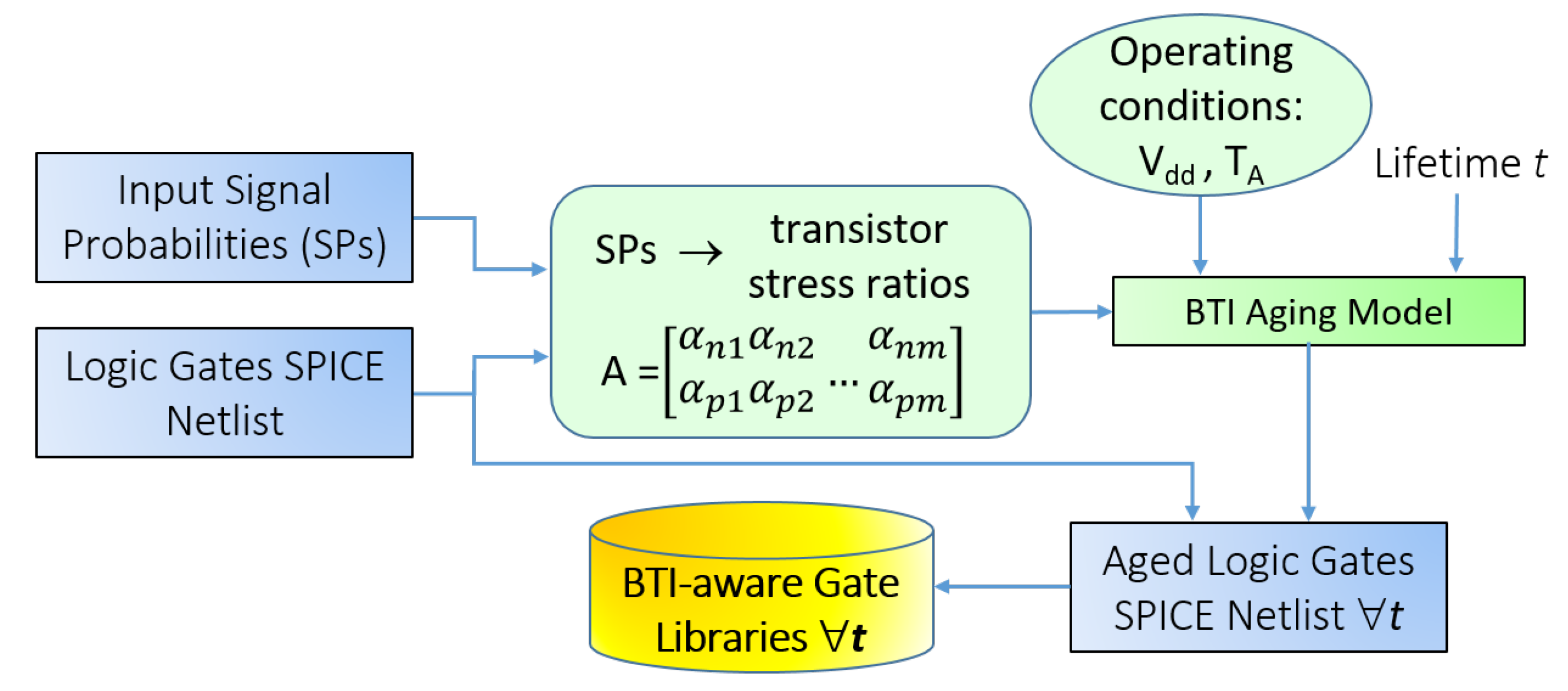
Figure 2 depicts the developed flow for evaluating the impact of the logic gate input signal probabilities on the stress ratios of their transistors, considering also the operating conditions (temperature and voltage) and lifetime. The obtained data for each gate were utilized to generate an “aged” library, which was then used to simulate complex circuits with all transistors mapped to the proper aging. The details are discussed in
Section 4.
The impact of temperature variations on aging and the evaluation of the effect of different DVFS operating modes on the system thermal profile were assessed by devising a simulation flow that takes data about the physical synthesis of a circuit and its input statistics as the input and then generates the power analysis of each considered DVFS mode as the output. This information, together with the circuit layout feed the HotSpot tool [
27], which performs a thermal analysis of each operating mode. The block diagram of the developed flow is shown in
Figure 3.
By exploiting the proposed simulation flows to evaluate the electric stress and thermal profile of a circuit, designers can accurately estimate the aging degradation of a circuit and assess its impact on the lifetime and reliability, as well as explore the reliability and performance trade-offs by selecting different DVFS operating modes. A 32 nm high-k metal-gate, CMOS technology from [
26] was considered for analysis and validation throughout the paper.
3.3. Stress-Induced BTI Variability
This subsection first discusses the stress-induced BTI variability generated by different signal probabilities reflected on the propagation delay of basic logic gates, thus logic paths, and their
variability. In the case of a NOT gate, results are shown in
Figure 4a,b for normalized propagation delay and
, respectively. The normalization factor is the delay exhibited by a logic gate at Time 0 (
).
Propagation delay was evaluated as the time interval elapsing between the instant at which the NOT input voltage experiences 50% of its full excursion, which is equal to
, and the instant at which the NOT output voltage performs the correspondent 50% variation, which is still equal to
. Denoting by
and
the input and output voltage of the NOT gate, respectively, the expression of propagation delay
can be formalized as follows:
It should be considered that all gates have been designed to be symmetric at ; therefore, either a or transition can be considered to evaluate the propagation delay for a fresh NOT. Instead, for aged gates, the propagation delay depends on the threshold voltage degradation, and thus on the input statistics. In this case, the propagation delay was measured in the worst-case conditions.
As for lifetime
, it was evaluated as the time interval required for the propagation delay to degrade by 15% over the value at
[
32]. In doing so, it was assumed that the clock period was determined by considering the worst-case propagation delay increased by 15% in order to account for possible effects due to PVT variations. If the propagation delay exceeds this margin, then an incorrect signal propagation takes place, thus possibly causing a system failure. Therefore,
at a generic operating time
t is evaluated as:
Figure 4, which was obtained considering input signal probability values
, 0.5, and 0.75, clearly shows that, although the delay variation is very small, the
variation exceeds two years.
Figure 5 depicts the simulation results for the normalized propagation delay of basic logic gates NAND and NOR, with 2–4 inputs, for different values of the input probabilities. Namely, the two extreme cases
and
, together with the average case
,
= 2, 3, 4 were considered for the input probabilities. For all simulated gates and input probabilities, the delay degradation after only 6 mo of operation exceeds 50% of the overall degradation in 10 y of operation. It is interesting to note that delay degradation is dominated by pMOS transistors’ aging (
) and increases with the number of inputs for the NAND gate, whereas this decreases for the NOR gate. Indeed, the stress probability of series pMOS transistors in NOR gates diminishes noticeably with the increase in the number of inputs, as highlighted by the stress ratio expressions reported in
Table 2 and
Table 3. This consideration does not apply to the parallel pMOS transistors in the NAND gates.
Another important characteristic that is worth highlighting is the generally small variability of the delay degradation for different input probabilities and the noticeable difference between the degradation trend for the NAND and NOR gates. In order to better assess this variability, the following two metrics can be defined:
where
is the maximum difference of the propagation delay for different input probabilities and is given by
. Therefore,
represents the variability of the propagation delay for different input probabilities against the delay exhibited by the considered gate at
;
is instead the variability of the propagation delay for different input probabilities against the average case (
0.5). Values for the normalized propagation delays and defined variability metrics are reported in the first set of columns of
Table 4.
As can be seen, the variability is very limited for all basic gates, with a NOR gate exhibiting a variability that is sensibly lower than for a NAND gate for all number of inputs. In the case of a NAND gate, ranges from 0.86% at 1 y to 1.38% at 10 y for a 2-in gate and from 1.39% at 1 y to 2.27 at 10 y for a 4-in gate; as for a NOR gate, is 0.82% at 1 y and 1.27% at 10 y for a 2-in gate and less than 0.07% for all lifetime for a 4-in gate. Similar considerations apply to .
Although the delay variability with input probability is very small, the
variation can be considerably larger. Values for
and the corresponding variability are reported in the last four columns of
Table 4. The variability metric for
was evaluated as:
For NAND gates, ranges from 17% (two inputs) to 42.7% (four inputs), thus exhibiting a much larger variability than the propagation delay. For NOR gates, the variability evaluation turns out to be less meaningful. Indeed, a maximum value for equal to 10 y was considered, after which the design is no longer operational. As a result, values exceeding 10 y and the corresponding variability were not evaluated.
3.4. Temperature-Induced BTI Variability
So far, BTI and propagation delay variability as a function of workload-induced stress variability have been accounted for in aging simulation frameworks [
2]. However, workload impacts BTI variability not only due to (electric) stress, but also due to temperature. Indeed, different workloads induce different switching activities, hence distinct power dissipation values in different blocks/paths in the considered design. Consequently, a considerable temperature difference may be exhibited by the blocks/paths in a design, which may exceed
[
27]. In addition, the operating frequency and voltage, which do not affect the stress ratio [
6], are the main players in determining the power consumption, thus the thermal profile of a design. Therefore, in a DVFS design, different operating modes are characterized by different thermal profiles and, consequently, by a different BTI aging. It should be noted that the operating modes of a DVFS design are usually controlled by a DTM system, which is responsible for monitoring online the circuit temperature through on-chip sensors. Moreover, it selects appropriately its operating mode (operating frequency and power supply) in order to honor pre-defined constraints, such as temperature, which is proportional to the power dissipation, and performance.
As an example, the Ethernet circuit from the IWLS 2005 benchmark suite was synthesized, which implements a DVFS technique with two operating modes, referred to as
low performance (
= 0.5 GHz@0.7 V) and
high performance (
= 2 GHz@1 V). Although the circuit is equipped with a DTM system selecting the proper DVFS operating mode at run-time, a fixed operating mode (either LP or HP) was assumed to better emphasize the impact of DVFS on the circuit thermal profile, and thus on BTI aging. The steady-state thermal analysis results for both LP and HP modes are shown in
Figure 6a,b, respectively.
For LP mode, the maximum temperature (hotspot) is approximately C, while reaches for HP mode. In particular, the hotspot is experienced in the upper area of the circuit in HP operating mode, due to the higher dynamic power dissipation of the random logic implementing the Rx and Tx cores that are located in that area, compared to the memory in the lower part of the circuit. On the other hand, in LP mode, the hotspot is localized in the lower part, since in this case, the leakage power of the memory prevails over the dynamic power of the random logic.
If the DTM policies are ignored during the lifetime estimation of the circuit, then either the temperature during LP or that during HP will be used. In the first case, the lifetime estimation may be very optimistic, whereas in the second case, very pessimistic. However, a circuit is meant to operate under the influence of the DTM system, whose policies determine the temperature variability, which should be properly considered for lifetime estimation during circuit design.
To better assess the impact of temperature on aging and, as a consequence, on propagation delay and lifetime, the same basic gates as in
Section 3.1 were considered. As an example, assume that the operating temperature is bounded in the interval [50, 100]
by the DTM system. In
Figure 7, the temperature-induced BTI variability that reflects on the
and
variability is pictured for a NOT gate (
Figure 7a) and for two-input NAND and NOR gates (
Figure 7b,c, respectively). As for the temperature, the upper and lower bounds were considered, as well as the average case (
). The signal probability was set to 0.5 in all cases. Detailed results for the Ethernet benchmark are presented in
Section 5. As can be seen, the effect of the temperature-induced BTI variability on propagation delay is higher than the stress-induced variability.
In
Table 5, temperature-induced variability values for three- and four-input basic logic gates are reported. As for propagation delay, variabilities
and
were evaluated as follows:
where
is the maximum propagation delay difference induced by different aging temperatures
and given by
. Variability
is calculated over the delay of a fresh device, whereas variability
is evaluated over the value of the propagation delay at
. Instead, lifetime variability is:
Comparing the results in
Figure 7 and
Table 5 to those in
Figure 4 and
Figure 5, it can be noticed that the effect of temperature-induced BTI variability exceeds the stress-induced one for both propagation delay and lifetime.
As conclusive remarks for the performed analyses, it can be observed that during the BTI-aware timing analysis of a DVFS design, which is crucial for evaluating its performance degradation and the expected lifetime, the contribution of temperature variability can be considerably higher than the contribution of stress variability. Therefore, both the stress and temperature variability induced by the workload should be considered during BTI-aware timing analysis. Nevertheless, if the workload is not known and the average case for input probability is considered, the error in propagation delay degradation due to aging is negligible, even though the corresponding error in lifetime estimation can be larger than 10%. Moreover, different operating modes exhibit very different thermal profiles, which implies that thermal management constraints should also be considered for the evaluation of temperature-induced BTI variability and its impact on lifetime and performance.
5. Simulations and Results
The developed simulation framework was applied to analyze the BTI degradation of the largest benchmark from the IWLS’05 suite [
28], the Ethernet benchmark. The synthesis of the benchmark was conducted with a 32 nm high-
k metal gate CMOS technology [
26] with DVFS using two operating modes, referred to as
low performance (
= 0.5 GHz@0.7V) and
high performance (
= 2 GHz@1V), as introduced in
Section 3. Finally, based on the results for various dynamic thermal management (DTM) constraints, the appropriate constraints were selected, which met either the lifetime or performance requirements. For the evaluation of the performance, the results of the thermal analysis regarding the utilization of each operating mode were used. Consider again the example presented in
Section 4 (
Figure 9). Once the thermal analysis had been conducted, the time that the circuit spent in either the HP or the LP operating mode,
and
(shown in
Figure 9), respectively, was obtained. Then, the expected long-term performance of the circuit was evaluated with the
effective operating frequency as:
In
Figure 10, the average temperature of the Ethernet circuit is presented. The considered dynamic thermal management (DTM) constraints were
and
. Note that for this case, the temperature window
w (
Figure 9) was
. The average temperature of the circuit at the hotspot was slightly higher than
, while the average temperature of all the gates of the longest path was
.
The propagation delay of the longest path for the considered temperatures is shown in
Figure 11. In particular, in
Figure 11a, propagation delay trend over time is depicted for the following operating temperatures: low DTM constraint
=
; high DTM constraint
=
; average temperature of the DTM constraints
=
+
; fine-grained temperature
, whose distribution throughout the circuit is shown in the thermal map in
Figure 10.
Figure 11b shows a zoom-in to highlight the region where the propagation delay curves cross the guard band considered to estimate the circuit lifetime
, which was set equal to
to have a long enough lifetime for all considered temperatures. A margin-based temperature selection for aging evaluation, either using the DTM constraints
or
, resulted in a lifetime estimation of
= 4.41 y and
= 2.01 y, respectively. If the average temperature
of the DTM constraints was instead considered, the lifetime estimation would be
=
y, which was expected to be more accurate than the estimation based on margin temperature selection. Finally, when all gates in the longest path were mapped with the fine-grained temperature
using the proposed framework, and thus the proper temperature was assigned to each gate, the lifetime estimation was
= 3.25 y. As a result, an optimistic evaluation using the
temperature underestimated the detrimental effect of BTI aging on the lifetime of the circuit, which turned out to be overestimated by 35.8% compared with the lifetime value obtained by using fine-grained temperature mapping,
. The estimation was instead pessimistic when using the
temperature, since it led to overestimating the actual effect of BTI on the circuit lifetime, thus underestimating the lifetime by
when compared with
. Even when the average temperature
was considered, the BTI effect on the lifetime of the circuit was overestimated by 4.8%.
Next, we show that the deviation between the lifetime
,
and
estimated considering DTM constraints
,
and average temperature
, respectively, against the lifetime obtained with the proposed framework
depends on the window size
. In
Figure 11c,d, the trend over time of the longest path propagation delay is depicted for
and
(
w =
). From
Figure 11d, the following values for the lifetime were derived:
y,
y,
y, and
y. Therefore, an optimistic evaluation using the
temperature underestimated the detrimental effect of BTI on the lifetime of the circuit by 61.9% and a pessimistic one using the
temperature overestimated it by
. Additionally, when the average temperature
between the two marginal constraints was considered, the BTI effect on the lifetime of the circuit was overestimated by 26.1%.
In
Table 6, results on the performance and lifetime obtained from the proposed fine-grained approach for DTM constraints with
(
) are reported. The first set of columns present results obtained considering
and
such that
, while the results in the second set of columns were obtained with
. For
, it can be observed that the
of the circuit increases with the increase of
w. This was attributed to a performance reduction that was also observed while
w increased. The reason for these trends was that the selected average temperature (
) caused a higher utilization of the LP operating mode. Since the sensor is located where the hotspot of the circuit is, it overestimated the average temperature of the circuit and forced an even higher utilization of LP operating mode than what would be necessary to meet the desired temperature constraints. For the higher average temperature (
), the exact opposite trend was observed.
dropped as
w increased and the performance increased, which was attributed to the already very high utilization of HP mode at those temperatures.
Figure 12 shows the results enabling design exploration in terms of
performance (
Figure 12a) and
lifetime (
Figure 12b), as a function of temperature constraints [
], for all possible temperature couples in the range [70
–150
], with
, that is the hot temperature
was set to be at least
higher than the cold temperature
.
The lifetime (left “y”-axis) and performance (right “y”-axis) results evaluated by using the developed fine-grained framework are depicted in
Figure 13a (solid lines) for a temperature window
w (“x”-axis) that gradually increases in size in the range [70
–150
]. It also depicts the estimated lifetime and performance when the average temperature of the marginal DTM constraints
is considered (dashed lines labeled as “LT@TA” and “Perf@TA”). Additionally,
Figure 13b shows the estimation errors for the examined temperature constraints if the average temperature
is considered and compared against the proposed approach based on a fine-grained temperature map
. Lifetime was evaluated as discussed in
Section 3.3, and the lifetime error is calculated as follows:
An analogous expression was used to calculate performance error. It is worth noting that at lower temperatures and while
w increased, the underestimation of the lifetime using the average temperature
also increased, reaching 35.8% for
. At higher temperatures, the lifetime can be overestimated by more than 10% for
. Similarly,
Figure 13c depicts the error in the performance estimation. At lower temperatures and while
w increased, the expected performance was overestimated by more than 20% for
, reaching 26.3% for
. At very high temperatures, the performance was slightly underestimated, with a difference lower than 1.2% over the fine-grained evaluation.
Next, possible trade-offs of various DTM constraints between lifetime and performance were examined.
Figure 14a depicts the results for the constraints with a temperature window
sliding in the range [70
–150
]. As the window slid towards higher temperatures, the performance increased almost linearly, due to the HP operating mode being utilized more, as expected. At the same time, the lifetime dropped asymptotically towards zero.
Figure 14b plots the relative error when comparing the lifetime prediction
against the lifetime
computed by the proposed framework. The longest path was considered, and the lifetime estimation error was computed as in (
11). The error was negative at lower temperatures, indicating that the lifetime estimation was optimistic, and became positive at higher temperatures, implying that it was pessimistic in this range.
Figure 14c,d presents similar results for DTM constraints with
. Note that these results were consistent with those in
Figure 13 and showed that, as
w increased, the error of lifetime estimation using marginal, or even the average expected temperature, also increased and a fine-grained temperature consideration was required, which was only possible using the proposed framework.


