1. Introduction
Since its beginning, integrated circuit (IC) technology has evolved significantly in several aspects: First, the range of circuits has been expanding continuously to target digital and analog, wired and wireless/RF, and low-power and medium-power applications. Second, the complexity of the realized functions have never stopped growing, which adds difficulties and more technical challenges for the circuit designer. Finally, the fabrication of ICs has diversified significantly with more than a dozen different processes currently available in bipolar, MOS, and BiCMOS technologies [
1].
On the other hand, digital integrated circuits have increased in integration density and speed, reaching several billions of transistors in one mm
of area and achieving Tera floating point operations per second (TFLOPS). Although they realize less complex functions than digital circuits, analog circuits are considered more challenging since their performance is more dependent on the dimensions of the transistors and passive components (i.e., width and length), as well as on the intended fabrication process and bias conditions. Consequently, long design cycles are the main bottleneck in analog IC design. Digital circuits benefit from many flexible and substantially automated electronic design software tools, in addition to pre-sized ready-to-use logic libraries that speed up their design phase [
2], whereas analog ICs still lack such a high degree of automation and rely significantly on the experience and skills of the engineer designing the circuit. One interesting way to alleviate this challenge is to design analog circuits by relying only on digital logic gates [
3,
4]. This allows the use of digital flow for analog circuit design, which drastically reduces the design time and effort. However, the performance obtained by these approaches, especially in terms of power consumption, are not yet as competitive as in classical analog design approaches.
As a matter of fact, once the system-level architecture and specifications are determined, analog design generally consists of choosing first the topologies for the basic building blocks such as amplifiers, oscillators, or comparators and then sizing the devices (transistors and passive components) of these building blocks to achieve a set of performance specifications.
This sizing step is challenging due to three major reasons: First, there are always multiple solutions to the same problem, which are usually spread in the space of possibilities. Second, the circuit performance is sensitive to uncontrollable random variations of the fabrication process [
1,
5] and temperature. Third, analog circuits are usually difficult to specify with a few performance metrics, which leads in some cases to more than a dozen of specifications to meet [
6,
7,
8] before a circuit designer is fully satisfied. Finally, some specifications are dynamic in the sense that they depend on the circuit conditions [
9], and therefore, some performance metrics could be degraded during the IC life-cycle, which renders the design even more complex.
In the past ten years, a considerable amount of research work has been conducted to enhance the automation level of analog IC design using machine learning (ML). The corresponding prior state-of-the-art can be split into three main categories.
Neural networks (NNs) of different complexities (shallow and deep) using both supervised [
10,
11,
12,
13,
14,
15,
16,
17,
18] and reinforcement [
19,
20,
21] learning techniques have been proposed in the past six years. These methods have been boosted by the progress in the development of high-performance computing hardware and are gaining attention in the scientific community thanks to their ability to model complex nonlinear problems [
22];
Multi-objective optimization with several heuristic- and stochastic-assisted strategies to explore the search space efficiently: Bayesian [
23,
24], particle swarm [
25], the Gaussian process [
26], simulated annealing [
27], and genetic algorithms [
28,
29,
30]. These are simulation-based optimizations that rely on a circuit simulator to find a solution. Although global optimization is not an ML technique in the strict sense of the word, it remains a powerful mathematical tool for the automation of circuit design. In contrast, older equation-based techniques as in [
31] are no longer considered;
Hybrid methods combining global optimization and NN were proposed in [
32,
33,
34,
35,
36,
37]. These techniques achieve enhanced results compared to pure multi-objective optimization methods, at a lower computation time.
In this work, we aimed to survey and investigate the recent progress made in the past six years in applying ML methods to analog IC front-end design automation exclusively. Techniques that use surrogate modeling [
38] instead of SPICE-like simulators were not included. Moreover, contributions targeting device modeling, physical back-end IC design [
39], and fault testing were not included in this paper. Instead, the focus was on the existing methods and innovations that have been proposed in the fields of supervised and reinforcement deep learning for front-end analog IC design. The working principles of the employed techniques, as well as some of their pros and cons are also discussed. The contributions of this work were: (1) to provide answers on which circuits and to which extent ML techniques were effectively used to help analog designers achieve good results; (2) to elaborate on the existing limitations that require further investigations in the field, as well as relevant future research directions.
There are some existing surveys in the literature that have tackled IC design automation [
40,
41,
42]. Nevertheless, they differ from the proposed survey in this paper. The authors in [
42] pointed out the recent advancements in the usage of deep convolutional neural networks and graph-based neural networks to accelerate the digital IC design workflow. Their survey covered ML-assisted micro-architectural space exploration (from high-level RTL design), physical back-end design (layout) for power optimization and estimation, critical IR drops in routes, and efficient placement. Thus, they focused on the digital VLSI flow and did not target analog circuits.
In [
40], a general high-level review of ML applications was provided in multiple areas of IC design from device modeling, front-end synthesis, and layout (back-end) design to fault testing. The work is well organized and provides a wide overview of the prior state-of-the-art without focusing particularly on one area.
The work in [
41] is another example of a high-level paper that surveyed a wide spectrum of artificial intelligence (AI) methods including knowledge-based and equation-based optimization techniques. In addition to sizing, the work covered performance modeling, which predicts the circuit performance dependency on device-level variations (e.g.,
,
), as well as IC yield optimization under process variation (i.e., corners). Finally, the paper spanned two decades of analysis in its presentation and covered digital along with analog design.
Therefore, the current work is, to the best of our knowledge, the first survey in the literature to focus particularly on recent (post-2015) ML-assisted analog front-end IC design automation, propose a profound level of understanding of the problem, and discuss the details of the key contributions from prior state-of-the-art and the effectiveness of the employed methods.
This paper is organized as follows: The existing NN-based automation approaches for analog IC design are detailed in
Section 2. Hybrid techniques are explained in
Section 3.
Section 4 provides a comparative analysis of the prior state-of-the-art, while
Section 5 covers the remaining open challenges and the most promising research directions to be explored in the field.
2. NN-Based IC Design Automation Methods
In this section, we elaborate on the various approaches that exist in the literature from the past six years to automate analog IC front-end design. Those techniques rely exclusively on ML, namely supervised and reinforcement learning using NNs. For completeness, we also expose the papers that present hybrid techniques. The explanatory details, effectiveness, range of applicability, and advantages of each method are given.
The use of NNs to solve complex practical problems has proven to be very efficient in numerous fields [
22]: speech recognition, medical imaging diagnosis, robotic vehicles, natural language processing, and image recognition. For such problems, mathematical modeling by equations is not possible because the designer cannot anticipate all situations, nor their changes over time, and in some cases, the designer even lacks knowledge on how to build the model itself.
The general idea of NNs is to build a model that approximates the real solution for a problem based on limited, yet sufficient, available dataset (training phase). At the same time, the model should be able to generalize and predict new outputs for previously unseen data (testing phase) with sufficient accuracy. NNs are very efficient at solving nonlinear problems due to their structure, which mimics the human brain’s activity, and their flexibility in adjusting the model’s complexity by removing or adding layers and neurons [
43].
The idea of using NNs to assist in analog circuit design was validated in 2003 for the case of operational amplifiers (opamp), as shown in [
44]. In the coming sub-sections, we elaborate on the use of NNs for analog IC front-end design and sizing in the two cases of supervised and reinforcement learning methods.
2.1. Supervised Learning
The core idea here is to gather a collection of input/output examples for the studied problem (the dataset), before trying to build an approximate solution. The efficiency of supervised learning is usually acquired through a large and labeled training dataset, which might be a limiting factor in problems where large labeled datasets are not available.
Previous attempts have been made to apply the NN supervised learning approach to design basic circuits. For example, in [
11], a small five-transistor inverter-based current comparator was designed using
CMOS technology, using a small network with 20 neurons that was trained with just 1500 examples to predict a few device sizes. In [
10], the authors developed an NN that can re-design an existing 4 bit current-steering DAC for the same target specifications, but in a novel technology node (
CMOS). Although scalable, this solution cannot be generalized to predict sizes for new, different specifications. The transient power consumption of a relaxation oscillator was modeled in [
18] using a 60-neuron time-delay NN, to enhance the circuit’s functional model during system-level verification. This approach was focused on power consumption and is well suited for mixed-signal blocks, which are usually modeled in behavioral languages.
Analog ICs implementing more complex functions (e.g., amplification, filtering) require more elaborate studies, larger training datasets, and networks with higher complexities in terms of layers and neurons.
In order to discuss the existing work in the literature, which applies supervised learning to analog IC design automation, a set of criteria for evaluating the prior state-of-the-art should be defined. In this work, the following criteria are proposed for this purpose:
Dataset generation technique;
Feature selection;
NN complexity;
IC fabrication process used;
Types of circuits targeted;
Result validation method.
2.1.1. Dataset Generation Technique
The dimensions of all transistors and passives (W, L), as well as reference currents and voltages (
,
) in an analog block are referred to, in this paper, as the design parameters
, while the circuit’s performance metrics (e.g., gain, power consumption, etc.) are called the specifications
. To build a model capable of predicting
, the initial step in supervised learning is to generate a dataset of circuit simulation results that covers the design space sufficiently. Analog designers must define the performance specifications, then simulate the circuit using a computer-aided design (CAD) tool for a significant number of possibilities of the design parameters, as shown in
Figure 1. The generation of such a dataset is a time-consuming task that involves people with a decent level of experience and knowledge in IC CAD tools. References [
13,
16] used SPICE circuit simulators to generate their datasets.
To illustrate how a dataset looks, we considered a basic source-coupled differential pair, with an active load, tail current mirror (equal-length devices), and a known-value resistor for biasing (see
Figure 2). Due to symmetry, only four transistors need to be sized (width, length), and thus, there are seven design parameters
.
Assume for simplicity that the amplifier to be designed is specified only for the following performance: differential voltage gain and power consumption. Consequently,
, and the combined vector
represents a single entry in the dataset, which is an
matrix where
N is the number of examples.
Table 1 shows two examples from the dataset of the previous circuit (dimensions in
,
in
).
On the other hand, there are no strict rules that define how many data are required for each type of circuit. Usually, more data are helpful (since this increases the model accuracy); nevertheless, in the case of analog IC design automation, the designer will generate only a reasonable amount of data to keep the task practical and time manageable. For example, 20,000 examples (dataset size) were needed in [
13] to train the NN and predict results for a similar circuit that was designed in [
14,
15] using only 9000 and 16,600 different examples, respectively. On the other hand, only 1600 data points were sufficient in [
12]. However, the previous numbers cannot be directly compared since the way the datasets were generated out of circuit simulators differed significantly from one study to the other. It is hence insightful to look into the different methods used to generate the training examples.
In [
14], the authors manually adjusted, prior to simulation, all MOS transistors sizes in order to obtain an initial valid solution that achieved proper performance (from a circuit designer’s perspective). This initial adjustment was made by circuit designers. Only then, the initial design parameters were slightly varied by 5%, and the different corresponding circuits were simulated one by one to extract their performance and build the dataset. Moreover, all transistors’ lengths L were fixed to 1
to reduce the design space and avoid short-channel effects. Therefore, the dataset in [
14] was too dependent on a pre-sized state of the circuit.
Reference [
13] proposed a similar, yet different approach for dataset generation: Initial values for the design parameters (
) were first determined by a circuit designer. Next, 100 different patterns were produced by randomly varying
in the range ±30%. The obtained circuits were then simulated, and a score was calculated to select the best circuit that had the highest score among all. The score was defined as the ratio of higher-the-better performance metrics in the numerator and lower-the-better in the denominator. This process was iterated as many times as needed to build the dataset, with the best circuit from the previous 100 patterns being the starting circuit for the generation of the next 100 patterns. The whole process is depicted in
Figure 3.
This approach had better exploration capabilities than [
14] thanks to its higher range of variation (30%); nevertheless, the selection of a solution at each step was dictated by a single score that compressed the valuable information contained in a set of performances to a unique metric. Moreover, the dataset used in training the NN depended somewhat on a pre-defined state of the circuit.
The authors in [
15] presented two novel ideas in data generation: First, they used an existing dataset from previous optimizations made by analog designers, which contained optimal or quasi-optimal circuits. The motivation here was to make the training data as accurate as possible by having in the examples only the design parameter values that guaranteed good performance. Second, the dataset was augmented by exploiting the fact that some specifications correspond to inequalities. When a circuit is required to have a power consumption below a specified threshold, all solutions resulting in a lower power consumption values were considered compliant and hence added to the set of examples. Therefore, the authors in [
15] artificially increased the dataset size by randomly generating additional examples with the same design parameters, but lower or higher (inequality) performance values.
In [
16], the dataset was generated from a special software framework (MaxFit GA-SPICE), based on a genetic multi-objective optimization algorithm that relied on a set of predefined circuit equations, which were developed by analog circuit designers. Therefore, the circuit performances for all examples had a high level of confidence and were highly accurate, since they were produced by a previous study. Nevertheless, this approach entirely relied on the accuracy and availability of the aforementioned software framework. Moreover, the generated dataset was further filtered to remove any outlier values, which were values exceeding three-times the standard deviation from the mean value (as defined in [
16]).
The work in [
17] proposed an interesting approach to widen the prediction range for the target performance, by generating a fully random dataset from a normal distribution on all design parameters. Some restrictions were rightly added to ensure quality examples and improve the model’s accuracy.
Table 2 summarizes the details of the different dataset-generation techniques used in the aforementioned studies.
2.1.2. Feature Selection
After dataset generation, the aim is to make the NN compute and converge towards a model that predicts the design parameters from the existing performance specifications . The neural network is asked, in this sense, to solve an inverse problem using a dataset generated from a direct problem definition.
The training phase is a standard ML process that requires a proper definition of the features or inputs from which the NN will learn. Normally, these can be the circuit performance metrics directly taken from the CAD simulators such as differential and common-mode gains in amplifiers, unity-gain–bandwidth, and power consumption, as in [
13,
14,
16]. A typical block diagram showing the input and output variables for the NN core used for analog IC design is represented in
Figure 4.
The NN features may also be expanded by
nth-order polynomial combinations as in [
15], where fourteen different combinations of second-order terms were generated from four simulated performance metrics only. In [
18] also, the same feature was sampled
d times before feeding it to the NN. A two-step approach wherein three behavioral features were considered separately for training, then recomposed into a single output in a later stage was adopted in [
12].
It is crucial that feature selection be left to experienced analog circuit designers who know well what, how, and to what extent each performance is linked to the design parameters. This step dictates how accurately the model will converge. To illustrate this, assume that a designer is building a model for an opamp using its open-loop voltage gain without including the performance features that are related to the high-frequency gain behavior (phase margin and gain–bandwidth product). Thus, the predicted design may experience instability once the opamp circuit is used in a closed-loop configuration. Another aspect that is worth discussion is the optimal number of features that need to be included in a dataset. From an ML perspective, more relevant features are usually welcomed since this pushes the neural network to build a more informed model. From a circuit designer perspective, performance metrics have different levels of importance. For example, a passive mixer’s total harmonic distortion (THD) might be more important to learn than its noise performance. Nevertheless, adding relevant and uncorrelated circuit features will certainly help the NN build a more accurate model, regardless of their importance.
2.1.3. NN Complexity
The NN structure and complexity must be carefully defined with the optimal number of layers and neurons per layer, to start the training process. There is no defined rule for this choice. It may vary substantially depending on the realized circuit function, the transistor count, the number of features (
) and their polynomial combinations (if any), as well as the size of the generated dataset. In IC design automation, the first layer has a number of inputs equal to the number of features, while the number of neurons in the output layer must match the number of design parameters to be predicted. In the middle, hidden layers are inserted to model complex nonlinear combinations of the circuit features, and this is where each NN should be customized for the intended circuit. Some good guidelines in this sense are the following: (1) for complex circuits (i.e., transistor count), a high number of neurons is required in each Layer; (2) when the combination of several performance metrics in a circuit contains useful information that needs to be included in the model, a high number of layers should be used to allow the NN to learn those effects. Nevertheless, adding more neurons and/or layers always comes with a longer training time.
Table 3 summarizes the prior state-of-the-art NN complexities implemented in supervised learning.
For example, the work in [
15] used three hidden layers with 120, 240, and 60 neurons, respectively, while in [
16], the authors opted for a single hidden layer with just nine neurons because the training examples were pre-sized ones. On the other hand, and since the dataset was randomly generated in [
14], which led to widely spread values in the design space, a much more complex network composed of 15 layers with 1024 neurons each was designed to obtain accurate results (
Table 3). This major difference stems from the simple observation that a low-complexity NN training on highly accurate datasets can learn as good as complex networks do on random data.
2.1.4. IC Fabrication Process
The training dataset depends heavily on the models of the transistors and passives that were used in the CAD simulations, which differ significantly from one fabrication process to another. Consequently, the same circuit topology with the same target specifications will result in different sets of design parameters depending on the intended IC fabrication technology. In [
13,
14], circuits were designed and verified in sub-micron CMOS processes (< 1
), although the exact transistor’s minimum length was not stated in the papers. On the other hand, the authors in [
15,
16] worked on
and
CMOS standard technologies, respectively. All previous work included both NMOS and PMOS transistor types in the circuits; however, there is no available study that investigates bipolar transistors and non-standard IC technologies such as SOI or BiCMOS.
2.1.5. Target Circuits
Analog circuits are extremely diversified currently, and they are designed to realize a variety of functions ranging from signal amplification, filtering, shaping, and clipping, to frequency mixing and many others. Therefore, the choice is very wide for the target circuit on which to apply the supervised ML approach. An intuitive decision is to opt for a structure that is easily reused in numerous systems, such as opamps, since their theory of operation is well known and they have the widest application range in analog systems [
1]. In fact, opamps are usually specified and designed as single open-loop circuits to be reused extensively in closed-loop systems. The automatic sizing of all the opamp components provides a huge benefit to circuit designers since they can focus more on the optimization of their macro-system performance and architecture decisions.
In [
14,
16], the same two-stage opamp circuit was used in the supervised ML approach. It corresponds to an NMOS source-coupled pair followed by a PMOS common-source. The biasing was realized by a simple resistor, thus exhibiting large process, supply voltage, and temperature variations.
In [
13], the authors used a very similar circuit, only replacing each transistor with its complementary type (PMOS vs. NMOS). Both circuits are valid opamps, although analog designers have a slight preference for the PMOS input devices, in order to minimize noise and optimize unity-gain frequency [
45]. All three previously studied circuits have differential inputs, but single-ended output structures.
A slightly different circuit was investigated in [
15], having differential outputs and using voltage combiners for biasing.
An interesting case is the CMOS band-gap voltage reference studied in [
12]. It includes an amplifier, with additional MOS transistors, diodes, and resistors. It represents a different type of analog circuit compared to [
13,
16] with the particularity of providing a supply- and temperature-independent DC voltage.
It is worth noting that previous work focused mainly on opamps and all had moderate circuit complexity (transistor count < 12).
2.1.6. Result Validation Method
Usually, after the NN has been trained on all examples, the standard way to validate the results is to generate a small set of new input/output examples that are not part of the original dataset. The new outputs, called the test-set performance metrics, are fed to the inputs of the NN, which in turn computes the corresponding design parameters according to the model built during the training phase. Next, those predicted NN outputs are fed back to the circuit simulator to obtain the predicted performance metrics. At this stage, a comparison is possible between the initial test-set performance and the predicted one (for each metric), then the mean relative error on all test examples is calculated to quantify the accuracy of the results.
Table 4 summarizes the accuracy of the results obtained in [
13,
16]. A comparison among the common specifications that were computed is theoretically sound, since all previous papers studied very similar circuits (two-stage CMOS opamp). The prediction error for each specification is computed using Equation (
1).
is the
jth performance metric estimated using a circuit simulator from the schematic that contains the NN-predicted design parameters
. On the other hand,
is the
jth performance metric that was initially input to the NN to make the prediction. For example, the gain and slew rate metrics in [
13] had a mean prediction error of 1.1% and 19.1%, respectively, according to
Table 4. The overall performance of a circuit is the combined effect of each of its predefined metrics, and therefore, it is interesting to compute both the average
and standard deviation
of the mean error for each performance. All prior state-of-the-art works achieved a low average error <10%; however, from a circuit designer’s perspective, it is mandatory that each metric reaches a low mean error, and hence, a low
is highly desirable. The work in [
13] had the highest
and
computed on 12 target specifications because the training dataset was randomly generated with 30% variation and the selection of examples was based on a single score. On the other hand, the work in [
16] had the lowest values thanks to high-accuracy pre-sized circuit examples provided to the NN by a special software framework.
2.2. Reinforcement Learning
Reinforcement learning (RL) is a sub-field of machine learning where the agent learns to perform a specific task by reward and penalty. Unlike supervised learning, RL does not require a labeled dataset to train. The training is performed by making predictions and obtaining rewards for those predictions. Rewards should be higher when the prediction is closer to the real value and lower otherwise. The goal of the training phase is to learn a policy that maximizes the sum of all rewards.
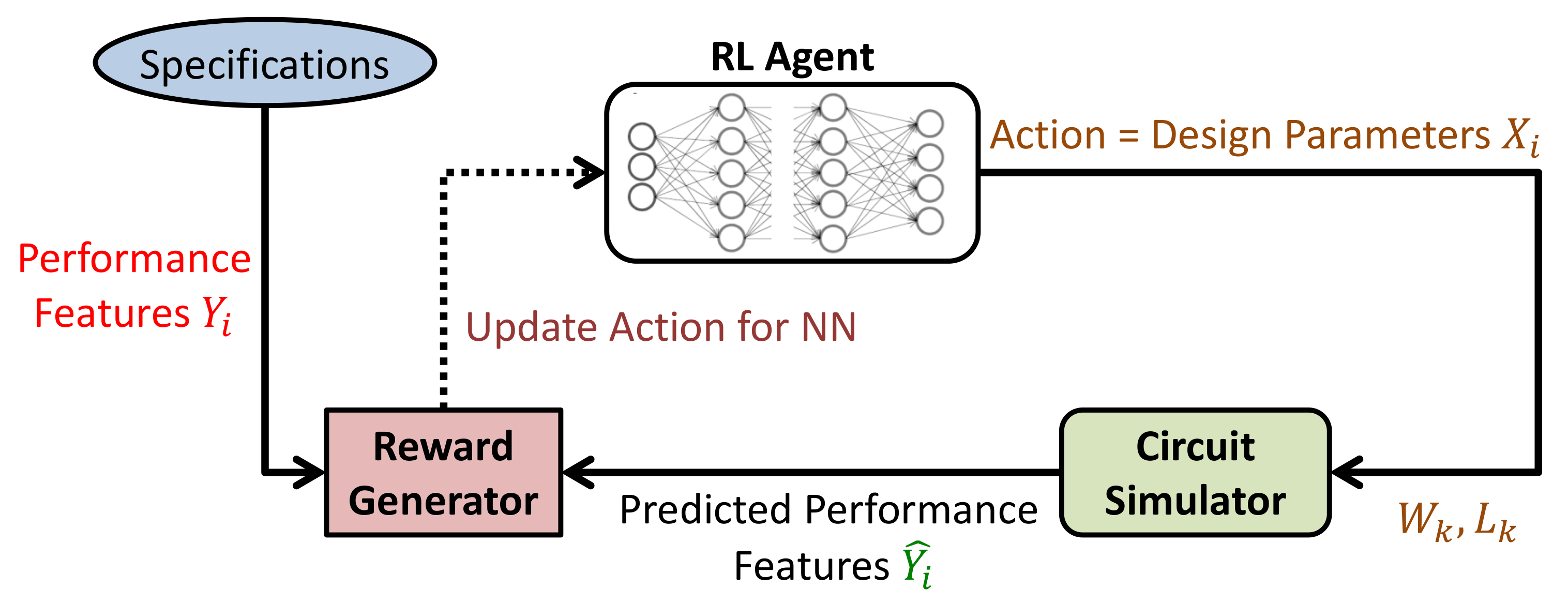
In IC design, RL is not extensively used yet. This section presents the previous work of four different teams who applied RL to solve analog IC design sizing problems. Before going into the details, it is worth pointing out the basics of RL in IC design. A vector of performance features represents the state of a circuit. The RL agent takes this vector as the input, executes an action by changing the design parameter values, computes the reward, then moves to the new state if the reward has increased and explores different available actions otherwise (
Figure 5). The reward is computed from the circuit simulator results.
Reference [
19] trained an RL agent for 30–40 h and achieved comparable or better performance than human experts on several circuits. The algorithm would output at each time step a set of values corresponding to the dimensions of the transistors and passive components (i.e., design parameters). The circuit simulation environment would then take those values and compute the performance metrics of the circuit. A reward function was defined based on hard design constraints, as well as good-to-have targets. The reward was formulated to be high if the simulated performance was close to the real values and low otherwise. Their approach was validated on two circuits: two- and three-stage transimpedance amplifiers in CMOS
. Five performance features were targeted: noise, gain, power consumption, AC response peaking, and bandwidth. In both circuits, RL showed promising results, where it outperformed the human experts in the time taken to find the optimal values.
On the other hand, a deep reinforcement learning framework was used in [
20] to find the circuit design parameters, as well as to gain knowledge of the design space. The algorithm found relevant solutions 40-times faster than regular genetic algorithm optimization. The approach was tested on a simple transimpedance amplifier and a two-stage opamp in CMOS 45
, then on another opamp with negative-gm load in FinFET 16
. On the first circuit, the algorithm converged 25-times faster than regular algorithms and was able to generalize well with
correct predictions out of 500 different target specifications. For the second and third circuits, it showed a speedup of 40-times over regular algorithms and predicted correctly
of 1000 and
of 500 different specifications.
The work in [
21] used deep RL to predict circuit design parameters as in the previous papers. However, the authors introduced a novel technique based on a symbolic analysis that rapidly evaluated the values of the DC gain and phase margin (PM) without invoking the circuit simulator. This process filtered out the most-likely bad states of the circuit and helped reduce the number of states that needed to be sent to the simulator for accurate performance prediction. Any set of design parameters that did not satisfy the DC gain and PM specifications were taken out of the loop early. Their system was tested on a folded-cascode opamp in CMOS 65
. The results did not show values for convergence speedup; nevertheless, the work was able to find sizing solutions correctly.
A promising work using a graph NN (GNN) and RL was presented in [
46]. The GNN achieved good prediction in applications where understanding the dependencies between related entities was important: chemistry (properties of molecules) and social networks (human interactions). The authors in [
46] exploited the fact that a circuit is not different from a graph where nodes are components and edges represent connections (i.e., wires). They implemented a convolutional GNN that processed the connection relationship between IC components and extracted features in order to transfer knowledge from one circuit to another. The proposed technique was capable of transferring knowledge between two slightly different topologies when they had some common design aspects (e.g., two-stage and three-stage amplifiers) or between two different fabrication process nodes of the same topology (e.g., CMOS 65
and 45
). For instance, the proposed RL algorithm learned to change the gain of a differential amplifier by tuning the dimensions of the input pair transistors. A successful demonstration on four circuits in CMOS
including amplifiers and low-dropout voltage regulators was presented. The problem was formulated to maximize a figure of merit (FoM), which was defined as the weighted sum of several performance metrics. Finally, porting of two sized circuits from one larger process node to several lower ones was achieved with shorter runtime.
3. Hybrid IC Design Automation Methods
In this section, existing work where two different automation techniques were used is presented. Since a combination of several methods leads to hybrid solutions that differ significantly, it is difficult to define common criteria to discuss them.
Reference [
33] proposed a two-step method targeting the re-design of existing analog circuits in new contexts. A context is a group of high-level conditions that impact the performance of an already pre-sized circuit (e.g., load, supply voltage values). The core idea is to use first a multivariate polynomial regression to estimate the performance trade-offs of the optimization and predict the circuit performance for the new context (which differ only moderately from the original ones). Then, the outputs are fed to an NN that trains itself from those updated examples to predict device sizes that correspond to the new performance (
Figure 6).
The previous two-step hybrid approach is a rapid tool for predicting (given a new circuit context) the sizing solutions corresponding to a near-optimal performance trade-off. A major aspect of this study was to benefit from existing designs and make an efficient reuse of them to predict the circuit performance under new conditions. The method was tested on a folded-cascode opamp with -biasing designed in CMOS . A re-design was made for new load capacitor values.
In [
32], the core idea was to delegate part of the NN design to a genetic algorithm (GA) that iterated to decide on the following: the neural network type (multi-layer perceptron or radial-basis function) and which performance metrics and which design constraints to include as the input features during training. The GA was actually given a set of performance specifications and some additional design constraints: the algorithm worked by feeding consecutively several subsets of the two previous variables to the NN, thus removing and adding input elements depending on the training and validation results. The best combination of NN type and set of features/constraints was selected as the optimal solution to perform the prediction of the circuit. One novelty in the proposed technique was that the constraints on the design parameters (to be predicted) were actually presented as additional inputs to the GA-NN combination to help reduce the level of under-determination. This hybrid approach was tested on a wide-band low-noise amplifier (LNA) based on a common-source cascode circuit with inductive degeneration, working at 3 GHz with input and output matching networks (see
Figure 7).
A novel learning framework based on evolutionary-algorithm optimization with an embedded neural network was proposed in [
34]. At each step of the optimization, a new design was derived from the previous (population-based method). The NN came into action only to assist in the sampling process that selected the best candidate design for the next generation. Predicting whether an offspring design was better than its parent was realized by a Bayesian NN that mimicked the circuit simulator with an additional benefit of being faster. In fact, it did not predict the circuit performance exactly; instead, it only classified two design samples (parent and current offspring) and output which one was better for each specification separately. The NN was trained progressively during the optimization and converged to stable weights quickly, since it only helped in increasing the sample efficiency (see
Figure 8). This novel method was tested on three different circuits: an amplifier similar to [
14], a two-stage opamp with negative-gm loads, and a mixed-signal system comprising an optical link receiver front-end. Moreover, layout parasitic effects were included in the prediction, which constituted a clear advantage.
A significantly different approach was used in [
35], wherein the objective was to reduce the convergence time of the evolutionary algorithm that predicted the circuits’ design parameters. Data produced from on-going optimization iterations were used to train an NN in parallel, in order to replace the time-consuming SPICE circuit simulators. Once the training was complete, the simulator was no longer used, and the NN would estimate the circuit performance rapidly, thus achieving quicker optimization results. The particularity of this work was that a separate NN was used for each performance specification. This hybrid method was successfully tested on a single-stage PMOS coupled-pair amplifier and a folded-cascode opamp with cascode loads and Vth biasing designed in
CMOS while achieving an ∼65% reduction in the execution time.
A time-efficient approach based on a genetic algorithm (GA) global optimization was adopted in [
37]. SPICE simulations were first used with the GA to cover the large space encountered in analog circuits, while a local minimum search for neighboring design regions was computed using a trained NN. The latter was progressively trained during the GA process, and once completed, it replaced the time-consuming circuit simulators for local regions only. The method was tested on a two-stage rail-to-rail opamp in CMOS
with a fifth-order Chebyshev active filter achieving <2% average error and a four-times speed improvement compared to classic evolutionary algorithms.
With the objective of decreasing the computation cost, the authors in [
36] used a Bayesian neural network (BNN) to model multiple circuit specifications by means of a novel training method (differential variational inference). The trained BNN was then introduced within a Bayesian optimization framework to capture the performance trade-off efficiently. The method was tested on a charge-pump circuit and a three-stage PMOS input device folded-cascode amplifier in 55
CMOS technology.
4. Discussion and Analysis
4.1. Analysis of the Previous Learning Approaches
Table 5 and
Table 6 provide a comparative summary of the studied prior state-of-the-art. Fabrication technology, input features, output design parameters, dataset size, and NN complexity were among the considered criteria. Another interesting aspect was the overall design time, which quantifies how long an ML agent needs to complete a circuit design as compared to humans. This time can be split into two parts: the dataset-generation and the NN training times. When applicable and available, these metrics are included in
Table 5 to provide some insights into the required design time. However, the hardware platform used for computation was rarely stated, which somewhat limits the conclusions. It is worth noting also that a straightforward estimation of the reliability of the presented techniques was difficult to obtain since each work had a different circuit, fabrication process, dataset size, and design parameters. Nevertheless, several important aspects of the comparison are presented in the coming paragraphs.
Usually, hybrid techniques rely on neural networks to assist the main optimization algorithm that actually performs the circuit-sizing task, either by reducing the operation time (replace the circuit simulator) or by helping to decide which exploration path to undertake. The software framework that hosts the whole process is hence complex, since a circuit simulator, a neural network, and a global optimization algorithm are required to communicate at the same time. In contrast, supervised and reinforcement methods rely on the NN to achieve the objective, and therefore, the framework is simpler to build, with the circuit simulator feeding its results to the NN in one step (supervised) or progressively (reinforcement). Moreover, the network complexity varies among the existing solutions for the same circuit being designed (
Table 5 and
Table 6).
The number of different circuit simulations that should be performed in the analog IC design (e.g., DC, AC, transient) is a bottleneck for the computation time. Some simulations are particularly time consuming such as the transient, while others are time efficient such as AC. Therefore, adding a new performance might lead to excessive simulation time and should be considered upfront during the problem definition. Circuits that require heavy transient simulations to be characterized are not well adapted to hybrid techniques that employ evolutionary algorithms, which are known to take an excessive time to converge. This point is worth considering when choosing between NN-based or hybrid techniques for a particular circuit.
The origin and reliability of a training dataset are crucial when using supervised learning in analog circuit design automation. How are the examples gathered? To what extent do they represent the full reality of the circuit? Answers to these questions determine the generalization capability of the obtained model, which guarantees that for new target specifications, we will obtain a set of relevant design parameters.
Some of the supervised learning techniques as in [
13,
14] constructed their dataset by randomly varying the design parameters in a close region around an initial solution corresponding to a pre-sized circuit with good performance. Thus, the NN model is highly correlated with this region within the overall design space, which raises questions on how good the predictions will be for solutions that are geometrically far in the design space from the initial one. Therefore, such a generation method creates local prediction models that are acceptable only if the intended application limits the circuit performance to a small region of the design space (opamps targeting audio applications always have low GBW values).
On the other hand, in [
15,
16], the dataset was collected from an existing database of solutions and, hence, depended totally on the availability and the validity of such an optimized set of examples. The dataset size may not be sufficient, nor is it possible to obtain on a wide range of circuits and fabrication technologies. Consequently, the computed model will have moderate generalization capability. To overcome this limitation, we recommend building a fully random dataset in order to cover the widest region in the overall design space.
On the other hand, hybrid methods rely on the wide exploration capability of the global optimization algorithms they employ (e.g., genetic) to cover the majority of the design space. Nevertheless, this comes at the cost of excessive simulation time and possible convergence issues.
A classification of all the studied machine learning techniques used in analog IC design in this paper is presented in
Figure 9.
The supervised learning technique is further divided into three sub-categories depending on how the dataset is being generated: using an existing pre-sized circuit database, by random generation in a close region around a predefined initial solution, or from a global normal distribution. On the other hand, hybrid techniques employ NNs for different purposes: replace the time-consuming IC simulators that slow down the global optimization or assist the algorithm itself by sampling or search exploration speedup. Finally, some hybrid methods use the genetic algorithm to design the optimal NN structure and to select the features for training.
Figure 10 shows the different exploration capabilities of the supervised learning and hybrid techniques studied in this work. Without loss of generality, a simplified two-dimensional representation of the design space was adopted. The wider the exploration within the design space, the higher the generalization of the computed model will be. Ideally, fully random dataset generation would cover the whole white space in
Figure 10 by sampling in multiple small regions spread over the entire design space, which is practically very difficult. Some randomized methods start by sampling over the whole design space before zooming-in on promising areas, which would help address this issue.
4.2. Analysis of Circuit Features
In analog circuit design, performance metrics are rarely equivalent in importance, nor are they similar in definition. For instance, an opamp’s phase margin (PM) is linked to its stability, and thus, no ML method has to match the specifications exactly to make the circuit stable. A higher PM than the target fixed by the circuit designer is highly desirable. On the other hand, a low-noise amplifier’s (LNA) gain specification must be met by equality, since lower gain values create poor noise behavior, whereas higher values result in bad linearity performance. Therefore, it is recommended to take into consideration this point during an ML algorithm’s implementation, by classifying the metrics into three types: lower, higher and hard feature. For example, in an LNA, the voltage gain must be processed as a hard feature, while its power consumption as a lower feature, meaning that reaching below the target is acceptable. Such domain-specific insights can be incorporated dynamically using logically inferred rules, as in [
47] or manually by domain experts, as is the case in the medical field.
In some cases, it is relevant to define two ways to measure the same performance depending on the input signal’s magnitude. For instance, the linearity of a voltage buffer should be measured by computing the full-scale (FS) THD in addition to the IIP3 figure. Thus, both metrics should be included in the training dataset; otherwise, the ML model will be limited to the small-signal behavior of the circuit and cannot predict accurate designs that meet FS requirements.
4.3. Transistor Biasing Considerations
When simulating to collect the training dataset, design parameters are often generated randomly, which leads to a high number of bad examples (poor performance) due to the inaccurate biasing of the transistors (see
Figure 10). Therefore, it is difficult for an ML technique to build a good model that contains such high variations in the input features. A way to overcome this limitation is to filter out (prior to training) all the examples for which the transistors are not in their intended region of operation, thereby reflecting the behavior of circuits accurately and allowing faster model convergence.
5. Open Challenges in the Field
Although the use of ML techniques to automate the analog IC design process has been a subject of intensive research recently, there are still topics that require further investigation in the field. In this section, we outline those research directions and point out relevant open challenges.
Despite the promising results obtained so far, there are very few studies in the prior state-of-the-art (if any) that deal with switched circuits. ML-assisted approaches to automatic sizing have not yet been explored for analog circuits in which transistors operate as switches. Mixers (both passive and Gilbert cell) and switched-capacitor filters (passive and opamp based structures) are widely used analog blocks that are interesting to investigate. Furthermore, from a circuit designer’s perspective, some aspects are still understudied. For example, in fully differential circuits, common-mode feedback (CMFB) loops are systematically used to control and adjust the common-mode output voltage for the optimal output swing. Only one paper in the prior state-of-the-art focused on fully differential structures, yet without including the CMFB loop. The latter poses additional constraints on the circuit stability and increases the overall transistor count and the number of design parameters, as well as the NN’s complexity.
One other open challenge is achieving an optimized multi-corner robust design. As is well known, process, voltage, and temperature (PVT) variations can lead to a significant performance drop and, in some cases, to a non-functional circuit. In a conventional approach, designers usually take margins with respect to the target specifications when sizing their blocks and then verify that their design is valid in all the corners. This approach requires fixing accurate margins for all specifications, since too large margins lead to over-sizing the circuit, while too small ones lead sometimes to redesigning. This approach could be used in the case of an ML-based design; however, it remains sub-optimal because the margins are chosen manually by the circuit designers. In [
48], the authors addressed the PVT challenge using a novel gravitational search algorithm. Nevertheless, their approach was able to find the most robust and feasible solution for an existing design only. Including this aspect in the ML algorithm from the beginning of the design phase would constitute an interesting contribution that would help reduce the design time.
Referring to
Table 5 and
Table 6, all the designed circuits in the prior state-of-the-art targeted CMOS technology exclusively. Moreover, they were designed using one library of transistors. The application of ML techniques to the design automation of circuits using multiple libraries such as low/standard/high
could be explored to widen the range of applicability of those methods. Applying ML techniques to design RF and analog circuits in BiCMOS, SOI, and other non-standard processes is another open challenge in the field. In the same line of thought, advanced CMOS technologies often exhibit many new effects that were not significant for older nodes. For example, an aspect such as shallow trench isolation should be integrated into the ML algorithm since it has a significant impact on the transistor performance, especially on the mobility and, as a consequence, on the threshold voltage [
27]. This would require integrating parameters such as the number of fingers and even information about the layout (form factor, number of dummy transistors, etc.) as design features. None of the existing studies have explored this research direction.
In all the previous surveyed papers, except for one example in [
34], analog circuits realizing one typical function were studied. An interesting and yet-unexplored research direction is to apply ML techniques to size and design an analog system composed of multiple building blocks. Analog-to-digital converters, digital-to-analog converters, track-and-hold amplifiers, and receiver and transmitter front-ends are good examples. The underlying benefit of such studies is to propose a flat-level optimization of the complete system using ML techniques, in contrast to the human expert approach and other hybrid approaches [
49], where a breakdown of the specifications per block is usually performed.


