Article

Broadband Class-J GaN Doherty Power Amplifier

1
Department of Electronics and Telecommunications, Politecnico di Torino, 10129 Turin, Italy
2
Department of Electronic, Faculty of Engineering, University of Zanjan, Zanjan 45371-38791, Iran
*
Author to whom correspondence should be addressed.
Electronics 2022, 11(4), 552; https://doi.org/10.3390/electronics11040552
Submission received: 21 December 2021 / Revised: 9 February 2022 / Accepted: 9 February 2022 / Published: 12 February 2022
(This article belongs to the Special Issue 5G Front-End Transceivers)

Abstract

:
This paper presents a broadband 3–3.7 GHz class-J Doherty power amplifier exploiting second harmonic tuning in the output network. Furthermore, the output impedance inverter is eliminated and its effect is embedded in the main device’s output matching network, thus trading off among bandwidth, efficiency, and gain. The proposed amplifier adopts two 10 W packaged GaN transistors, and it achieves in measurement 60–74%, and 46–50% drain efficiency at saturation and 6 dB output back-off, respectively, with a saturated output power of 43–44.2 dBm and a small-signal gain of 10–13 dB. The proposed DPA exhibits a simulated adjacent channel power ratio less than −30 dBc at 36 dBm average output power, when a 16-QAM modulation with 5 MHz bandwidth is applied to the 3.5 GHz carrier.

1. Introduction

Due to the increasingly growing demand for wireless communication systems with high quality and high data rates, the radio frequency (RF) transceiver is being pushed to operate at higher frequencies and wider bandwidths, and with modulation schemes characterized by high Peak-to-Average Power Ratios (PAPRs). The power amplifier (PA) strongly affects the performance of the transmitter [1,2,3], and thus it should operate as efficiently as possible over wide bandwidths, maintaining a sufficient level of linearity, which is especially challenging for 5G systems, based on Orthogonal Frequency Division Modulation (OFDM). OFDM signals have a varying envelope and high PAPR of the order of 10 dB to 12 dB for aggregated multicarrier signals [4], thus making the design of a PA that operates efficiently over wide dynamic and frequency ranges a critical challenge [5,6,7,8,9]. Crest Factor Reduction or Selected Mapping techniques [10,11] are normally adopted to reduce the PAPR of these signals to the 6 dB to 8 dB range, hence mitigating the negative effects of very high PAPR on the PA efficiency.
Nonetheless, in conventional PA architectures, the efficiency drops significantly when output power decreases with respect to its maximum value, where the efficiency is also maximum. This being a major drawback for non-constant envelope modulations, the efficiency enhancement in back-off has been addressed resorting to various techniques. These belong to two main categories, namely those based on supply modulation, such as envelope elimination restoration [12,13] and envelope tracking [14,15,16], and those exploiting load modulation [17]. The Doherty architecture [18,19,20], the Chireix outphasing [21,22,23], and the Load Modulated Power Amplifier (LMBA) [24,25] belong to the latter category. Among these PA architectures, the Doherty PA (DPA) has had a significant success thanks to its simplicity and ease of implementation in single-RF-input form, with a comparatively good intrinsic linearity [26]. Dual input DPAs have indeed also been explored [27,28,29], demonstrating superior performance compared to their single-input counterparts, but their appeal for real-field applications remains questionable due to the higher system complexity and cost.
One of the main challenges in the design of DPAs is achieving very wide bandwidths, which is hindered by several factors [30,31], among which it is worth mentioning the quarter wavelength transmission line that is used as an impedance inverting network (IIN) between the main device and the common node, the reactive parasitic effects of the active devices, and the possible presence of offset lines or narrowband post-matching networks.
Moreover, in order to enhance PA performance, harmonic tuning techniques have been considered so far [32,33,34], but most of them suffer from bandwidth limitations. The class-J PA shows wide bandwidth compared to other harmonic-tuned PAs [35,36,37], while its sensitivity to harmonics of the matching network is lower than class F [38,39].
In this paper, a wideband class-J DPA with high efficiency and linearity is designed using the CGH40010F GaN HEMT from Wolfspeed, targeting operation around 3.5 GHz, which is of interest for sub-6 GHz 5G applications.
The novelty of the proposed DPA is twofold: on one hand, the removal of the IIN on the main path and the embedding of the impedance inversion in the output matching network (OMN) improves the bandwidth, and on the other hand, the exploitation of the effect of the second harmonic allows us to keep gain and efficiency high over a 700 MHz bandwidth. The implemented class-J DPA achieves, in continuous wave (CW) measurement conditions, saturated and 6 dB output power back-off (OBO) efficiency of 60–74% and 46–50%, respectively, with an associated saturated output power of 43–44.2 dBm over the 3–3.7 GHz frequency range.
The structure of the paper is the following. In Section 2, the theory underlying the Doherty and class-J operation is discussed, and it is then applied to the proposed PA design in Section 3. Section 4 reports the simulation results, including linearity assessment. The measurement results are shown in Section 5, and finally, conclusions are drawn in Section 6.

2. Theoretical Analysis

This section reviews the theoretical foundations of the Doherty and class-J amplifiers, explaining how these concepts are exploited for the design of the proposed class-J DPA.

2.1. Doherty PA

The block diagram of a conventional class AB-C DPA is shown in Figure 1a, where the transistors are replaced by a simplified model composed of an ideal current generator and an output L C network, representing the reactive parasitic effects in the band of interest. In this work, two CGH40010F packages GaN HEMTs are adopted, whose parasitic elements are considered to be C P = 1.27 pF and L P = 0.73 nH [40].
The ideal scattering parameters of the cascade of the output parasitics of the device and its output matching network (OMN) are expressed as follows [41]:
A = [ S 11 S 12 S 21 S 22 ] = [ 0 e j ϕ e j ϕ 0 ]
where ϕ is the phase of S 21 , and the network is assumed lossless. Therefore, the load reflection coefficients at the intrinsic drain terminal of the main device can be expressed as [41]:
Γ M AB = S 11 + S 12 S 21 Γ M 1 1 S 22 Γ M 1 = Γ M 1 e j 2 ϕ
where Γ M 1 is the reflection coefficient before the IIN (a quarter wavelength line with characteristic impedance equal to R opt ) and it is expressed as:
Γ M 1 = Z M 1 R opt Z M 1 + R opt
where R opt represents the intrinsic optimum load of the class-AB main device, and Z M 1 is derived as follows:
Z M 1 = R opt ( 2 x )
The parameter x is the ratio between auxiliary and main current (x = I A / I M ), and the common node impedance is assumed to be equal to R opt / 2 . Substituting (3) and (4) into (2) leads to
Γ M AB = R opt ( 2 x ) R opt R opt ( 2 x ) + R opt e j 2 ϕ = 1 x 3 x e j 2 ϕ .
As shown in (5), Γ M AB is a function of x and θ . The presence of the IIN and the fact that the impedance at the common node of the Doherty combiner changes with frequency, limit the bandwidth of the DPA [42]. A possible solution to mitigate this issue is to remove the λ /4 line acting as IIN and designing the OMN of the main device so as to perform the impedance inversion required by the Doherty load modulation [32].
Furthermore, a conventional class AB-C DPA only considers the load at the fundamental frequency f 0 , and assumes a short-circuit termination at all higher harmonics. Since properly terminating the higher harmonics can significantly improve performance, in this design the OMNs have been designed to operate the devices in class J.

2.2. Class-J PA

The waveforms of the intrinsic drain current ( i D ) and drain-source voltage ( v DS ) of a class-J amplifier are described by the following equations [38]:
i D ( ω t ) = I max π + I max 2 cos ( ω t ) + 2 I max 3 π cos ( 2 ω t )
v DS ( ω t ) = V DD + ( V DD V K ) cos ( ω t ) α ( V DD V K ) sin ( ω t ) 0.5 α sin ( 2 ω t ) + . . .
where I max is the maximum current of the transistor, V K is its knee voltage, V DD is its supply voltage, and α is the empirical coefficient representing the reactive component of a class-J load, and it assumes values between −1 and +1.
By using Equations (6) and (7), the intrinsic impedance of the main device at saturation, at fundamental and second harmonic, can be derived as:
Z L ( f 0 ) = ( 1 + j α ) R opt
Z L ( 2 f 0 ) = j 3 π 8 α R opt .
In back-off, the drain current is expressed as follows [43]:
i D , OBO ( ω t ) = 1 γ I max π + I max 2 cos ( ω t ) 2 I max 3 π cos ( 2 ω t ) + . . .
where γ is the ratio between output power at saturation and at the selected OBO point ( γ = P out , sat / P out , OBO ). Therefore, adopting (7) and (10), the main OBO impedance at the fundamental frequency can be calculated as:
Z L , OBO ( f 0 ) = γ ( 1 + j α ) R opt .
The matching network design considering a variable load at both fundamental and second harmonic would be extremely difficult. Besides, in this case, the second harmonic impedance has a limited variation with power and is therefore assumed to be constant. The constant second harmonic impedance is expressed as follows:
Z L ( 2 f 0 ) = Z L , OBO ( 2 f 0 ) = Z L , sat ( 2 f 0 ) = j 3 π 8 α R opt
As shown in Equations (8), (9), (11) and (12), the fundamental impedance should have a resistive and a reactive component, the second harmonic impedance should be purely reactive, and the higher harmonics are assumed to be shorted at the transistor intrinsic drain plane.

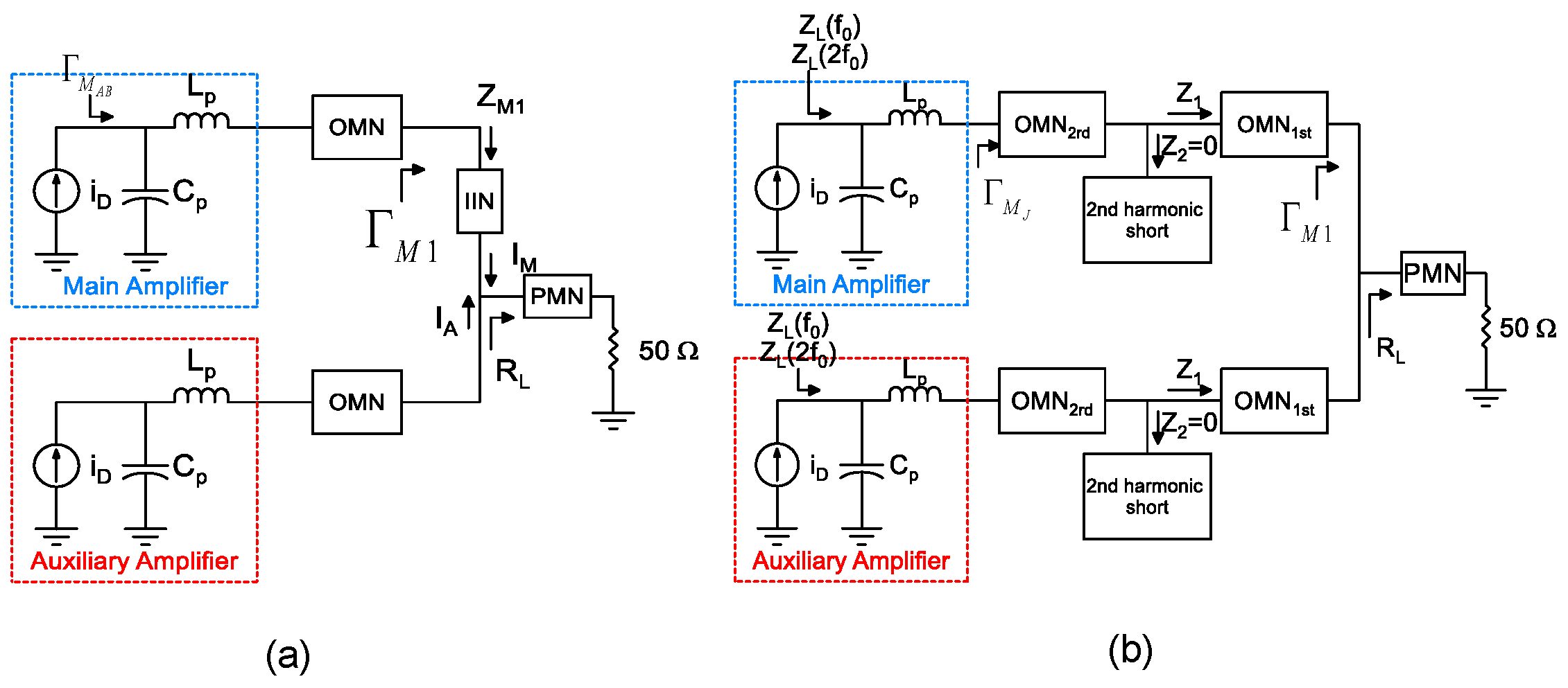
3. Class-J DPA Design Strategy

In order to achieve class-J operation for the main and auxiliary devices, their OMNs, which share the same structure, are designed in a modular way: in particular, each OMN is composed of three parts, as shown in Figure 1b. A second harmonic matching network (OMN 2nd), terminated by a second harmonic short (SC 2nd), synthesizes the proper impedance at the second harmonic, then the matching network OMN 1st sets the proper load at the fundamental frequency without affecting the second harmonic. Based on Equations (3) and (8), the intrinsic main reflection coefficient at fundamental for the class-J DPA can be written as:
Γ M J = R opt ( 2 x ) ( 1 + j α ) R opt R opt ( 2 x ) ( 1 + j α ) + R opt e j 2 ϕ = ( 2 x ) ( 1 + j α ) ( 2 x ) ( 1 + j α ) e j 2 ϕ
Based on Equation (13), the obtained class-J reflection coefficient is as a function of x, α , and ϕ , thus gives more degrees of freedom to design the output matching network with respect to the classical class-AB case. Figure 2 shows the impedance of class-J at the fundamental and second harmonics for R opt = 50 Ω . The real part of the fundamental impedance at OBO and saturation is constant, whereas the imaginary part changes from k R opt to + k R opt , where k equals 1 and 2 at saturation and at OBO, respectively.
According to Equations (6) and (7), the output power at fundamental frequency and the drain efficiency of our class-J PA are:
P out J = ( V DD V K ) 4 I max
D E J = P out J P DC = ( V DD V K ) 4 I max V DD I max π = π 4 1 V K V DD
Thus, P out J and D E J are independent of α . The dependency of the reflection coefficient Γ M J on α hence provides a degree of freedom to design the OMN, without compromising power and efficiency. In particular, in this work the value α = 0.5 , yielding to an optimum load for class-J operation R opt , J = 1.25 R opt , larger than the load resistance 2 R L .
Differently from a conventional DPA, which adopts a quarter-wavelength transmission line as IIN, the OMN of the proposed DPA embeds the impedance inversion too, which widens the bandwidth. In this work, a low pass matching network is used, shown in Figure 3. The capacitor C 1 is representative of the parasitic drain capacitance, and the inductance L 4 is exploited as drain bias feed. The Chebyshev theory [44] is used to calculate all elements of the OMN. The optimum bandwidth is achieved when the impedance ratios are:
R opt , J R 1 = R 1 R 2 = R 2 2 R L
where R 1 and R 2 are calculated as:
R 1 = 2 R opt , J 2 R L 3 R 2 = 4 R L 2 R opt , J 3
According to (16), the values of L and C of each of the three ladder networks, are given by:
L 1 = Q 1 R 1 ω , L 2 = Q 2 R 2 ω , L 3 = 2 Q 3 R L ω C 1 = Q 1 R opt , J ω , C 2 = Q 2 R 1 ω , C 3 = Q 3 R 2 ω
where Q 1 , Q 2 , and Q 3 are defined as:
Q 1 = R opt , J R 1 1 , Q 2 = R 1 R 2 1 , Q 3 = R 2 2 R L 1
Since C 1 is related to the parasitic of the transistor and has a constant value, Q 1 and R opt must be selected accordingly. The values of the OMN’s elements obtained from Equations (16)–(19) are illustrated in Table 1 for R L = 25 Ω and R opt , J = 62.5 Ω .
Since the implementation of the OMN with lumped capacitors and inductors is not applicable at the frequencies of interest, due to the low-quality factor of the Surface Mount Device (SMD) inductors, the equivalent distributed form, using microstrip lines is extracted. The capacitors are replaced by open-circuited stubs, while inductors are replaced by transmission lines. In this work, a Rogers RO4350B substrate ( ϵ r = 3.66, substrate height and metal thickness of 0.8 mm and 35 μ m, respectively) is used. The length of the transmission lines and stubs is calculated as [44]:
l line = ω L Z , l β
l stub = arctan ( 2 ω Z , c C ) β
where Z l and Z c are the characteristic impedance of the line for the inductor and capacitor and β is the propagation constant. The final output matching networks for the main and the auxiliary devices are shown in Figure 4a. Figure 4b shows the simulated internal output impedance of the main and auxiliary transistor, for the fundamental and second harmonic at saturation and at 6 dB OBO. As can be noted, the second harmonic impedance is constant in both cases, while the fundamental impedance is properly modulated by the power level.
The simulated drain current and drain-source voltage waveforms at saturation are demonstrated in Figure 5 at 3.5 GHz, confirming that the designed DPA generates the expected class-J-mode waveforms with quasi-half-sinusoidal current and voltage.
At the input, a parallel resistor–capacitor network ( R = 60   Ω , C = 3.3 pF) is inserted in series to the gate of each transistor for in- and out-of-band stabilization. The wideband input matching network (IMN) minimizes the input mismatch. Finally, an uneven 90 ° hybrid splitter feeds the input power to the main and auxiliary PAs with splitting ratio of P Aux / P Main = 1.5 .

4. Simulation Results

The DPA performance is evaluated in simulation in the frequency range 3–3.7 GHz, under the following operating conditions: V GM = 2.95 V, V GA = 6 V, V DD = 28 V, with a quiescent drain current of 112 mA. Figure 6 shows the CW simulation results of the drain efficiency and gain over the operating bandwidth.
A two-tone analysis is also performed at 3.5 GHz to evaluate the linearity of the DPA. The third and fifth order intermodulation distortion (IMD3 and IMD5), shown in Figure 7a versus output power, remain better than −20 dBc and −31 dBc, respectively, for P out < 43 dBm. In order to assess the system-level behavior, the DPA is simulated using a 16-QAM modulated signal and 6 dB PAPR. The input and output power spectrum at the center frequency of 3.5 GHz and with 5 MHz bandwidth are shown in Figure 7b. At an average output power of 36 dBm, the simulated ACPR is −30 dBc, and which is comparable to the results shown in [8,45].

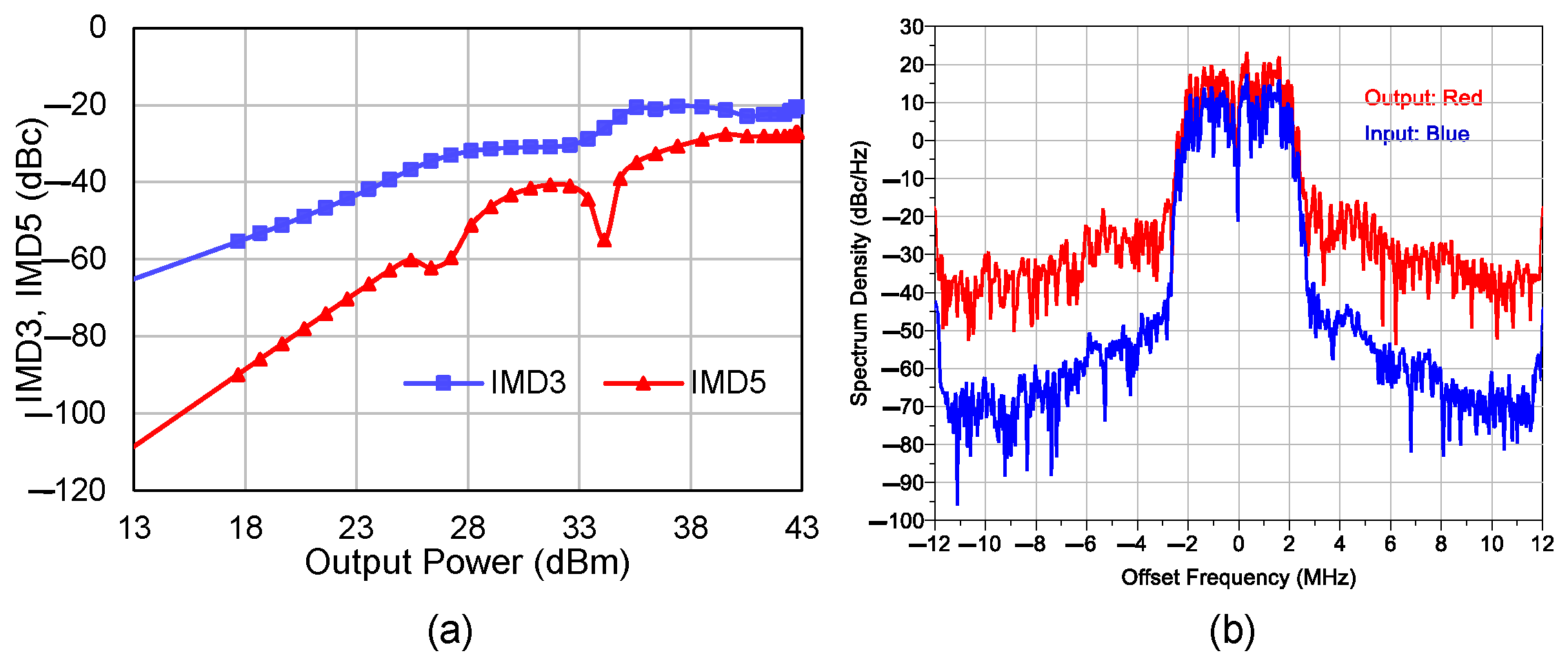
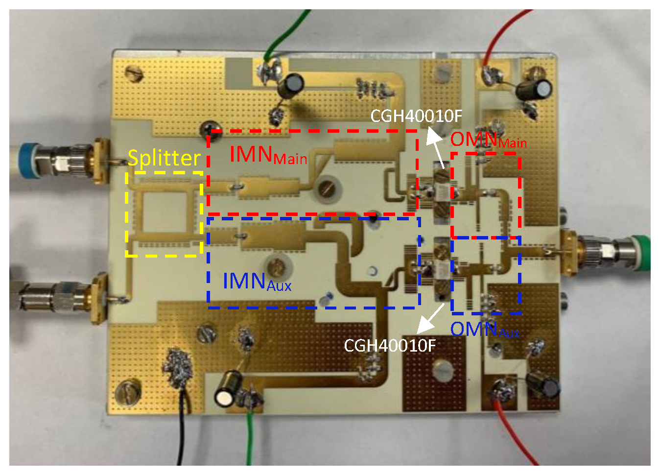
5. Measurement Results

Figure 8 shows the photograph of the proposed class-J Doherty PA. The amplifier has been characterized from 3 GHz to 3.7 GHz, in the following operating condition: V GM = 2.8 V, V GA = 6 V, V DD = 28 V, I D = 110 mA. The scattering parameters of the DPA are illustrated in Figure 9, showing a flat gain of around 12 dB over the target 700 MHz bandwidth, with S 11 and S 22 better than -10 dB, confirming also a good agreement between simulation and measurement.
The large-signal CW measurement results versus output power are shown in Figure 10. Power gain, drain efficiency, and output power versus frequency at saturation and at 6 dB OBO are illustrated in Figure 11. The drain efficiency is in the 60–74% range at saturation, while at 6 dB OBO, it is between 46% and 50%. The saturated output power is in the 43–44.2 dBm range.
The proposed class-J DPA is compared with other works in Table 2. The performance obtained is well in line with the state of the art in the target frequency range, thus demonstrating that the developed amplifier is suitable for 5G applications in the S-band.

6. Conclusions

In this paper, a wideband 20 W class-J Doherty PA with high efficiency and linearity is proposed for 5G applications, operating in the 3–3.7 GHz frequency range. Unlike conventional DPAs, the quarter-wavelength transmission line has been eliminated, embedding the impedance inversion in the output matching network, which also includes harmonic tuning to enable class-J operation. The saturated output power achieved in measurement is from 43 dBm to 44.2 dBm, while the drain efficiency at saturation and at 6 dB OBO are 46–50% and 60–74%, respectively.

Author Contributions

Formal analysis, A.N. and M.E.; methodology, A.N., M.E. and S.T.; resources, A.N., M.E., S.T. and A.P.; supervision, S.T., M.P., V.C. and C.R.; validation, S.T. and A.P.; writing—original draft, A.N. and M.E.; writing—review and editing, S.T., A.P., M.P., V.C. and C.R. All authors have read and agreed to the published version of the manuscript.

Funding

This research received no external funding.

Conflicts of Interest

The authors declare no conflict of interest.

References

  1. Naah, G.; He, S.; Shi, W.; Li, C. Symmetrical Doherty power amplifier design via continuous harmonic-tuned Class-J mode. AEU-Int. J. Electron. Commun. 2019, 106, 96–102. [Google Scholar] [CrossRef]
  2. Lopera, J.R.; Mayock, J.; Sun, Q.; Gadringer, M.; Bösch, W.; Leitgeb, E. A 3.5 GHz High Power GaN Hybrid Doherty Power Amplifier with Dynamic Input Power Splitting for Enhanced Power Added Efficiency at Backoff. In Proceedings of the 2021 IEEE Topical Conference on RF/Microwave Power Amplifiers for Radio and Wireless Applications (PAWR), San Diego, CA, USA, 17–20 January 2021; pp. 1–4. [Google Scholar] [CrossRef]
  3. Abbasnezhad, F.; Tayarani, M.; Abrishamifar, A.; Nayyeri, V. A simple and adjustable technique for effective linearization of power amplifiers using harmonic injection. IEEE Access 2021, 9, 37287–37296. [Google Scholar] [CrossRef]
  4. Baxley, R.J.; Zhao, C.; Zhou, G.T. Constrained Clipping for Crest Factor Reduction in OFDM. IEEE Trans. Broadcast. 2006, 52, 570–575. [Google Scholar] [CrossRef]
  5. Estebsari, M.; Nasri, A.; Piacibello, A.; Ramella, C.; Camarchia, V.; Pirola, M. 3.1–3.6 GHz 22 W GaN Doherty Power Amplifier. In Proceedings of the 2020 23rd International Microwave and Radar Conference (MIKON), Warsaw, Poland, 5–8 October 2020; pp. 424–426. [Google Scholar] [CrossRef]
  6. Hattab, G.; Ibnkahla, M. Multiband spectrum access: Great promises for future cognitive radio networks. Proc. IEEE 2014, 102, 282–306. [Google Scholar] [CrossRef] [Green Version]
  7. Nikandish, G.; Staszewski, R.B.; Zhu, A. Bandwidth enhancement of GaN MMIC Doherty power amplifiers using broadband transformer-based load modulation network. IEEE Access 2019, 7, 119844–119855. [Google Scholar] [CrossRef]
  8. Cheng, Z.; Xiong, G.; Liu, Y.; Zhang, T.; Tian, J.; Guo, Y.J. High-efficiency Doherty power amplifier with wide OPBO range for base station systems. IET Microwaves Antennas Propag. 2019, 13, 926–929. [Google Scholar] [CrossRef]
  9. Dehqan, A.; Toofan, S.; Medi, A. A highly efficient class-EF 2 power amplifier in GaAs pHEMT technology. Analog Integr. Circuits Signal Process. 2017, 93, 197–203. [Google Scholar] [CrossRef]
  10. Tani, K.; Medjahdi, Y.; Shaiek, H.; Zayani, R.; Roviras, D. PAPR reduction of post-OFDM waveforms contenders for 5G amp; Beyond using SLM and TR algorithms. In Proceedings of the 2018 25th International Conference on Telecommunications (ICT), Saint-Malo, France, 26–28 June 2018; pp. 104–109. [Google Scholar] [CrossRef]
  11. Rateb, A.M.; Labana, M. An Optimal Low Complexity PAPR Reduction Technique for Next Generation OFDM Systems. IEEE Access 2019, 7, 16406–16420. [Google Scholar] [CrossRef]
  12. Bolotov, A.; Kholyukov, R.; Varlamov, O. EER power amplifier modulator efficiency improvement using PWM with additional sigma-delta modulation. In Proceedings of the 2018 Systems of Signal Synchronization, Generating and Processing in Telecommunications (SYNCHROINFO), Minsk, Belarus, 4–5 July 2018; pp. 1–4. [Google Scholar] [CrossRef]
  13. Zheng, S.Y.; Liu, Z.W.; Pan, Y.M.; Wu, Y.; Chan, W.S.; Liu, Y. Bandpass filtering Doherty power amplifier with enhanced efficiency and wideband harmonic suppression. IEEE Trans. Circuits Syst. I Regul. Pap. 2016, 63, 337–346. [Google Scholar] [CrossRef]
  14. Jin, Q.; Ruan, X.; Ren, X.; Wang, Y.; Leng, Y.; Chi, K.T. Series–parallel-form switch-linear hybrid envelope-tracking power supply to achieve high efficiency. IEEE Trans. Ind. Electron. 2016, 64, 244–252. [Google Scholar] [CrossRef]
  15. Pergushev, A.; Sorotsky, V.; Ulanov, A. Criteria for selection envelope tracking power supply parameters for high peak-to-average power ratio applications. In Proceedings of the 2019 IEEE International Conference on Electrical Engineering and Photonics (EExPolytech), St. Petersburg, Russia, 17–18 October 2019; pp. 13–16. [Google Scholar] [CrossRef]
  16. Watkins, G.T.; Mimis, K. A 65% efficient envelope tracking radio-frequency power amplifier for orthogonal frequency division multiplex. IET Microw. Antennas Propag. 2015, 9, 676–681. [Google Scholar] [CrossRef]
  17. Ramella, C.; Piacibello, A.; Quaglia, R.; Camarchia, V.; Pirola, M. High efficiency power amplifiers for modern mobile communications: The load-modulation approach. Electronics 2017, 6, 96. [Google Scholar] [CrossRef] [Green Version]
  18. Gustafsson, D.; Andersson, C.; Fager, C. A modified Doherty power amplifier with extended bandwidth and reconfigurable efficiency. IEEE Trans. Microw. Theory Tech. 2013, 61, 533–542. [Google Scholar] [CrossRef]
  19. Quaglia, R.; Camarchia, V.; Moreno Rubio, J.J.; Pirola, M.; Ghione, G. A 4-W Doherty Power Amplifier in GaN MMIC Technology for 15-GHz Applications. IEEE Microw. Wirel. Compon. Lett. 2017, 27, 365–367. [Google Scholar] [CrossRef] [Green Version]
  20. Ramella, C.; Camarchia, V.; Piacibello, A.; Pirola, M.; Quaglia, R. Watt-Level 21–25-GHz Integrated Doherty Power Amplifier in GaAs Technology. IEEE Microw. Wirel. Compon. Lett. 2021, 31, 505–508. [Google Scholar] [CrossRef]
  21. Chang, H.C.; Roblin, P.; Galaviz-Aguilar, J.A.; Núñez Pérez, J.C.; Pond, R.; Xie, C.; Doo, S.J. Asymmetrically-driven current-based chireix class-F power amplifier designed using an embedding device model. In Proceedings of the 2017 IEEE MTT-S International Microwave Symposium (IMS), Honololu, HI, USA, 4–9 June 2017; pp. 940–943. [Google Scholar] [CrossRef]
  22. Cappello, T.; Barton, T.W.; Florian, C.; Litchfield, M.; Popovic, Z. Multilevel Supply-Modulated Chireix Outphasing With Continuous Input Modulation. IEEE Trans. Microw. Theory Tech. 2017, 65, 5231–5243. [Google Scholar] [CrossRef]
  23. Piacibello, A.; Quaglia, R.; Pirola, M.; Cripps, S. Design of an S-Band chireix outphasing power amplifier based on a systematic bandwidth limitation analysis. In Proceedings of the 2018 13th European Microwave Integrated Circuits Conference (EuMIC), Madrid, Spain, 23–25 September 2018; pp. 186–189. [Google Scholar] [CrossRef]
  24. Quaglia, R.; Cripps, S. A Load Modulated Balanced Amplifier for Telecom Applications. IEEE Trans. Microw. Theory Tech. 2018, 66, 1328–1338. [Google Scholar] [CrossRef] [Green Version]
  25. Pang, J.; Chu, C.; Li, Y.; Zhu, A. Broadband RF-Input Continuous-Mode Load-Modulated Balanced Power Amplifier With Input Phase Adjustment. IEEE Trans. Microw. Theory Tech. 2020, 68, 4466–4478. [Google Scholar] [CrossRef]
  26. Giofrè, R.; Colantonio, P.; Giannini, F.; Ramella, C.; Camarchia, V.; Iqbal, M.; Pirola, M.; Quaglia, R. A comprehensive comparison between GaN MMIC Doherty and combined class-AB power amplifiers for microwave radio links. Int. J. Microw. Wirel. Technol. 2016, 8, 673–681. [Google Scholar] [CrossRef]
  27. Andersson, C.M.; Gustafsson, D.; Cahuana, J.C.; Hellberg, R.; Fager, C. A 1–3-GHz Digitally Controlled Dual-RF Input Power-Amplifier Design Based on a Doherty-Outphasing Continuum Analysis. IEEE Trans. Microw. Theory Tech. 2013, 61, 3743–3752. [Google Scholar] [CrossRef]
  28. Kalyan, R.; Rawat, K.; Koul, S.K. A digitally assisted dual-input dual-band Doherty power amplifier with enhanced efficiency and linearity. IEEE Trans. Circuits Syst. II Express Briefs 2018, 66, 297–301. [Google Scholar] [CrossRef]
  29. Piacibello, A.; Quaglia, R.; Camarchia, V.; Ramella, C.; Pirola, M. Dual-input driving strategies for performance enhancement of a Doherty power amplifier. In Proceedings of the 2018 IEEE MTT-S International Wireless Symposium (IWS), Chengdu, China, 6–10 May 2018; pp. 1–4. [Google Scholar] [CrossRef]
  30. Camarchia, V.; Piacibello, A.; Quaglia, R. Integrated Doherty power amplifiers for satellite Systems: Challenges and solutions. In Proceedings of the 2019 IEEE Topical Workshop on Internet of Space (TWIOS), Orlando, FL, USA, 20–23 January 2019; pp. 1–4. [Google Scholar] [CrossRef]
  31. Chen, S.; Wang, G.; Cheng, Z.; Xue, Q. A bandwidth enhanced Doherty power amplifier with a compact output combiner. IEEE Microw. Wirel. Components Lett. 2016, 26, 434–436. [Google Scholar] [CrossRef]
  32. Fang, J.; Moreno, J.; Quaglia, R.; Camarchia, V.; Pirola, M.; Guerrieri, S.D.; Ramella, C.; Ghione, G. 3.5 GHz WiMAX GaN Doherty power amplifier with second harmonic tuning. Microw. Opt. Technol. Lett. 2012, 54, 2601–2605. [Google Scholar] [CrossRef]
  33. Wang, T.; Cheng, Z.; Liu, G. Highly efficient Doherty power amplifier using continuous inverse class-F and class-J hybrid mode. Int. J. RF Microw. Comput.-Aided Eng. 2020, 30, e22464. [Google Scholar] [CrossRef]
  34. Naah, G.; He, S.; Shi, W.; Li, C.; Nusenu, S.Y. Harmonic-tuned continuum mode active load modulation output combiner for the design of broadband asymmetric Doherty power amplifiers. IET Microw. Antennas Propag. 2019, 13, 1226–1234. [Google Scholar] [CrossRef]
  35. Huang, C.; He, S.; You, F. Design of broadband modified class-J Doherty power amplifier with specific second harmonic terminations. IEEE Access 2017, 6, 2531–2540. [Google Scholar] [CrossRef]
  36. Nasri, A.; Estebsari, M.; Toofan, S.; Piacibello, A.; Ramella, C.; Camarchia, V.; Pirola, M. A 3–3.8 GHz Class-J GaN HEMT Power Amplifier. In Proceedings of the 2020 23rd International Microwave and Radar Conference (MIKON), Warsaw, Poland, 5–8 October 2020; pp. 416–419. [Google Scholar] [CrossRef]
  37. Nikandish, G.; Staszewski, R.B.; Zhu, A. A broadband continuous class-F GaN MMIC PA using multi-resonance matching network. In Proceedings of the 2019 14th European Microwave Integrated Circuits Conference (EuMIC), Paris, France, 30 September–1 October 2019; pp. 108–111. [Google Scholar] [CrossRef]
  38. Alizadeh, A.; Frounchi, M.; Medi, A. Dual-band design of integrated class-J power amplifiers in GaAs pHEMT technology. IEEE Trans. Microw. Theory Tech. 2017, 65, 3034–3045. [Google Scholar] [CrossRef]
  39. Kim, J. Analysis and design optimisation for inverse Class-F GaN Doherty amplifier. IET Microw. Antennas Propag. 2019, 13, 448–454. [Google Scholar] [CrossRef]
  40. Rubio, J.M.; Fang, J.; Camarchia, V.; Quaglia, R.; Pirola, M.; Ghione, G. 3–3.6-GHz wideband GaN Doherty power amplifier exploiting output compensation stages. IEEE Trans. Microw. Theory Tech. 2012, 60, 2543–2548. [Google Scholar] [CrossRef]
  41. Li, C.; You, F.; Peng, J.; Wang, J.; Haider, M.F.; He, S. Co-design of matching sub-networks to realize broadband symmetrical Doherty with configurable back-off region. IEEE Trans. Circuits Syst. II Express Briefs 2019, 67, 1730–1734. [Google Scholar] [CrossRef]
  42. Nasri, A.; Estebsari, M.; Toofan, S.; Piacibello, A.; Pirola, M.; Camarchia, V.; Ramella, C. Design of a Wideband Doherty Power Amplifier with High Efficiency for 5G Application. Electronics 2021, 10, 873. [Google Scholar] [CrossRef]
  43. Zhang, H.; Zhan, R.Z.; Li, Y.C.; Mou, J. High Efficiency Doherty Power Amplifier Using Dual-Adaptive Biases. IEEE Trans. Circuits Syst. I Regul. Pap. 2020, 67, 2625–2634. [Google Scholar] [CrossRef]
  44. Pozar, D.M. Microwave Engineering; John Wiley & Sons: Hoboken, NJ, USA, 2011. [Google Scholar]
  45. Yu, C.; Su, Z.; Liu, Y.; Tang, B.; Li, S. Broadband filtering high-efficiency Doherty amplifier based on a novel post-matching network. In Proceedings of the 2019 European Microwave Conference in Central Europe (EuMCE), Prague, Czech Republic, 13–15 May 2019; pp. 212–215. [Google Scholar]
Figure 1. Schematic diagram of the (a) conventional DPA. (b) Proposed Class-J DPA.
Electronics 11 00552 g001
Figure 2. Intrinsic main and auxiliary impedances of the DPA class-J at the fundamental and second harmonics when R opt = 50 Ω .
Electronics 11 00552 g002
Figure 3. Low pass output matching network.
Electronics 11 00552 g003
Figure 4. (a) Schematic of the OMNs (dimension length and width are in millimeters), and (b) corresponding simulated fundamental and second harmonics load modulation for the main and auxiliary PAs.
Electronics 11 00552 g004
Figure 5. Simulated waveforms of the drain-source voltage and drain current at 3.5 GHz.
Electronics 11 00552 g005
Figure 6. Simulated (a) drain efficiency and (b) gain of the designed DPA versus output power.
Electronics 11 00552 g006
Figure 7. (a) Simulated IMD3 and IMD5 versus output power. (b) Simulated input (blue) and output (red) spectra at 3.5 GHz.
Electronics 11 00552 g007
Figure 8. Photograph of the fabricated class-J DPA.
Electronics 11 00552 g008
Figure 9. Measured and simulated scattering parameters of the proposed DPA.
Electronics 11 00552 g009
Figure 10. Measured CW performance of the DPA: (a) drain efficiency and (b) gain.
Electronics 11 00552 g010
Figure 11. Measured (dashed) and simulated (solid) CW performance of the proposed DPA versus frequency at saturation and at 6 dB OBO: (a) drain efficiency, (b) output power, and (c) gain.
Electronics 11 00552 g011
Table 1. Values of the OMN components.
Elements L 1 L 2 L 3 C 1 C 2 C 3
Value0.75 nH0.7 nH0.6 nH0.2 pF0.22 pF0.25 pF
Table 2. Comparison of the proposed class-J DPA with the literature: only designs based on the same CGH40010F device are considered.
Ref.Freq.
(GHz)
Pout
(dBm)
DE Sat.
(%)
DE OBO
(%)
Gain
(dB)
[1]1.45–2.4542–4448–64.236–526–13
[8]2.9–3.343.97040.6–44.26–11
[34]1.4–2.4541.8–43.547.5–64.235.5–526–13
[45]2.2–2.643–4460–6545–53-
[42]2.8–3.643–44.262–7644–568–13
[39]2.442.369.35412
[40]3–3.643–4455–6638–5612
This Work3–3.743–44.260–7446–5011–13
Publisher’s Note: MDPI stays neutral with regard to jurisdictional claims in published maps and institutional affiliations.

