Article

A 56 GS/s 8 Bit Time-Interleaved ADC in 28 nm CMOS

1
Institute of Microelectronics, Chinese Academy of Sciences, Beijing 100029, China
2
School of Microelectronics, University of Chinese Academy of Sciences, Beijing 100049, China
*
Authors to whom correspondence should be addressed.
Electronics 2022, 11(5), 688; https://doi.org/10.3390/electronics11050688
Submission received: 13 January 2022 / Revised: 9 February 2022 / Accepted: 21 February 2022 / Published: 23 February 2022
(This article belongs to the Section Circuit and Signal Processing)

Abstract

:
This paper presents a real-time output 56 GS/s 8 bit time-interleaved analog-to-digital converter (ADC), where the full-speed converted data are output by 16-lane transmitters. A 64-way 8 bit asynchronous SAR array using monotonous and split switching strategy with 1 bit redundancy is utilized to achieve a high linearity and high-power efficiency. A low-power ring voltage-controlled oscillator-based injection-locked phase-locked loop combining with a phase interpolator-based time-skew adjuster is developed to generate the 8 equally spaced sampling phases. Digital gain correction, digital-detection-analog-correction offset calibration, and coarse–fine two-step time-skew calibration are combined to optimize the ADC’s performances. An edge detector and phase selector associated with a common near-end data-transmission position and far-end data-collection instant are designed to avoid reset competition and implement deterministic latency. Fabricated in a 28 nm CMOS process, the prototype ADC achieves an outstanding SNDR of 36.38 dB at 56 GS/s with a 19.9 GHz input, where 7.25 dB and 9.33 dB are optimized by offset-gain calibration and time-skew calibration, respectively. The ADC core occupies an area of 1.2 mm2 and consumes 432 mW power consumption.

1. Introduction

Ultra-high sample rate analog-to-digital converters (ADCs) operating at several tens of gigahertz are increasingly demanded in leading-edge instruments, optical communications, multiple-input multiple-output (MIMO) systems, and 6G communications [1,2,3,4,5,6]. Benefiting from the technology scale and digital architecture, successive approximation register (SAR) ADC shows prominent advantages in power efficiency and area occupation for high-speed and moderate-resolution designs. Previous studies show that single-channel SAR ADC are suited for the designs that operate at around 1 GS/s with 6–8b resolution [7,8,9,10]. In order to achieve a sampling rate at several tens of gigahertz, the time-interleaved (TI) SAR architecture becomes a dominant solution [11,12,13,14,15,16].
Y. M. Greshishcheva et al. reported a 6 b 40 GS/s ADC with power dissipation <1.5 W utilizing interleaved SAR ADCs. It employs an on-chip 128 K memory along with an on-board PC interface for data processing and ADC characterization [17]. L. Kull et al. implemented a 24–72 GS/s 8 bit TI-SAR ADC with on chip gain and time-skew calibration, where their coefficients were obtained by off-line calculation utilizing the stored data in the memory [18]. K. Sun et al. designed a 56 GS/s 8 bit TI-SAR ADC with foreground calibration employing an off-line algorithm to calculate the coefficients for the offset, gain, and time skew [19]. However, these designs mainly focus on the ADC core with on-chip memory and partial data output, which cannot achieve high calibration accuracy and implement real-time data output. In addition, they all utilize a power-hungry current mode logic (CML) divider-chain to generate multi-sampling clocks, hence suffering from severe bandwidth limitation and great power consumption. For real-time data output, deterministic latency plays a vital role to implement precise data collection and multi-chip synchronization.
To address these issues, this paper presents a 56 GS/s 8 bit time-interleaved ADC with 16-lane 28 Gb/s transmitters. A low-power ring voltage-controlled oscillator (RVCO)-based injection-locked phase-locked loop (IL-PLL) combined with a phase interpolator (PI)-based time-skew adjuster is developed to generate the 8 equally spaced sampling phases. A dedicated analog–digital hybrid calibration scheme is developed to calibrate the comparator offset, gain error, and time skews. An edge detector and phase selector associated with a common near-end data transmission position and far-end data collection instant are designated to implement the deterministic latency.
This paper is structured as follows: Section 2 describes the chip architecture; Section 3 explains the ADC implementation; Section 4 presents the ADC calibration algorithm; Section 5 introduces the deterministic latency and synchronization in detail; Section 6 shows the measured results; and Section 7 draws the conclusion.

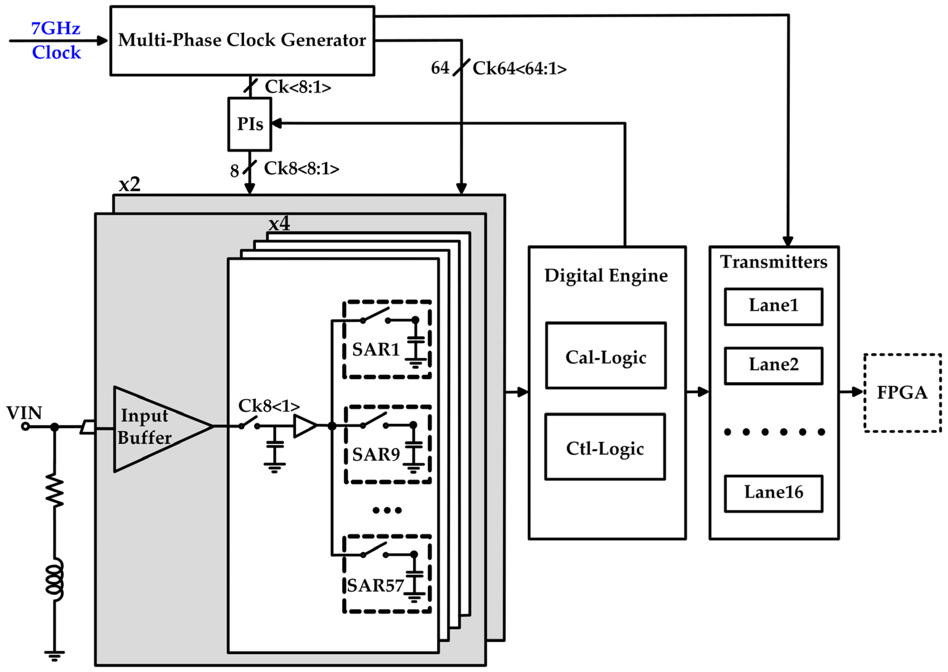
2. Chip Architecture

Figure 1 shows the block diagram of the designed prototype chip, including a 56 GS/s 8 bit TI-ADC core, a multi-phase clock generator (MPCG), a digital engine, and 16-lane serial transmitters. The 56 GS/s 8 bit ADC core consists of the even and odd 28 GS/s ADCs. Each employs a separate driving input buffer to protect the input signal of the 28 GS/s ADC from the influence of clock feedthrough coming from the other ADC. The 28 GS/s ADC adopts a 4 × 8 two stage sampling front-end to trade off the sampling speed and input bandwidth, where the first-stage sampler operates at 7 GS/s and the second-stage samplers located in the sub-SARs run at 875 MS/s. Specifically, the analog input signal is first buffered and then sequentially sampled onto the sampling capacitors by 4 NMOS sampling switches. Each sampled voltage is further applied to 8-way interleaved sampling SAR ADCs. The MPCG produces the 8-phase 7 GHz clocks (Ck8<8:1>) with a 25% duty cycle, which define the sampling time of track and hold circuits (T/Hs) and 64-phase 875 MHz clocks (Ck64<64:1>) with about 12.5% duty cycle, which define the sampling time of SAR ADCs. The digital engine contains the calibration logic (Cal-Logic) for the ADC and control logic (Ctl-Logic) for data transmission. Here, the Cal-logic performs two functions. The first is offset and time-skew error detection that are fed back to the ADC core to implement the offset and coarse time-skew calibration. The second is gain calibration. The calibrated data are applied to the Ctl-Logic, which are first scrambled and then first-input first-output (FIFO) to the physical transmitters. The transmitters serialize the parallel data to sequences and drive them to an off-chip FPGA, which performs fine time-skew calibration utilizing a proposed fractional delay filter algorithm. The 16-lane transmitters operating at 28 Gb/s are utilized to output the converted data of the 64 SAR ADCs operating at 875 MS/s with 8 bit parallel data.

3. ADC Implementation

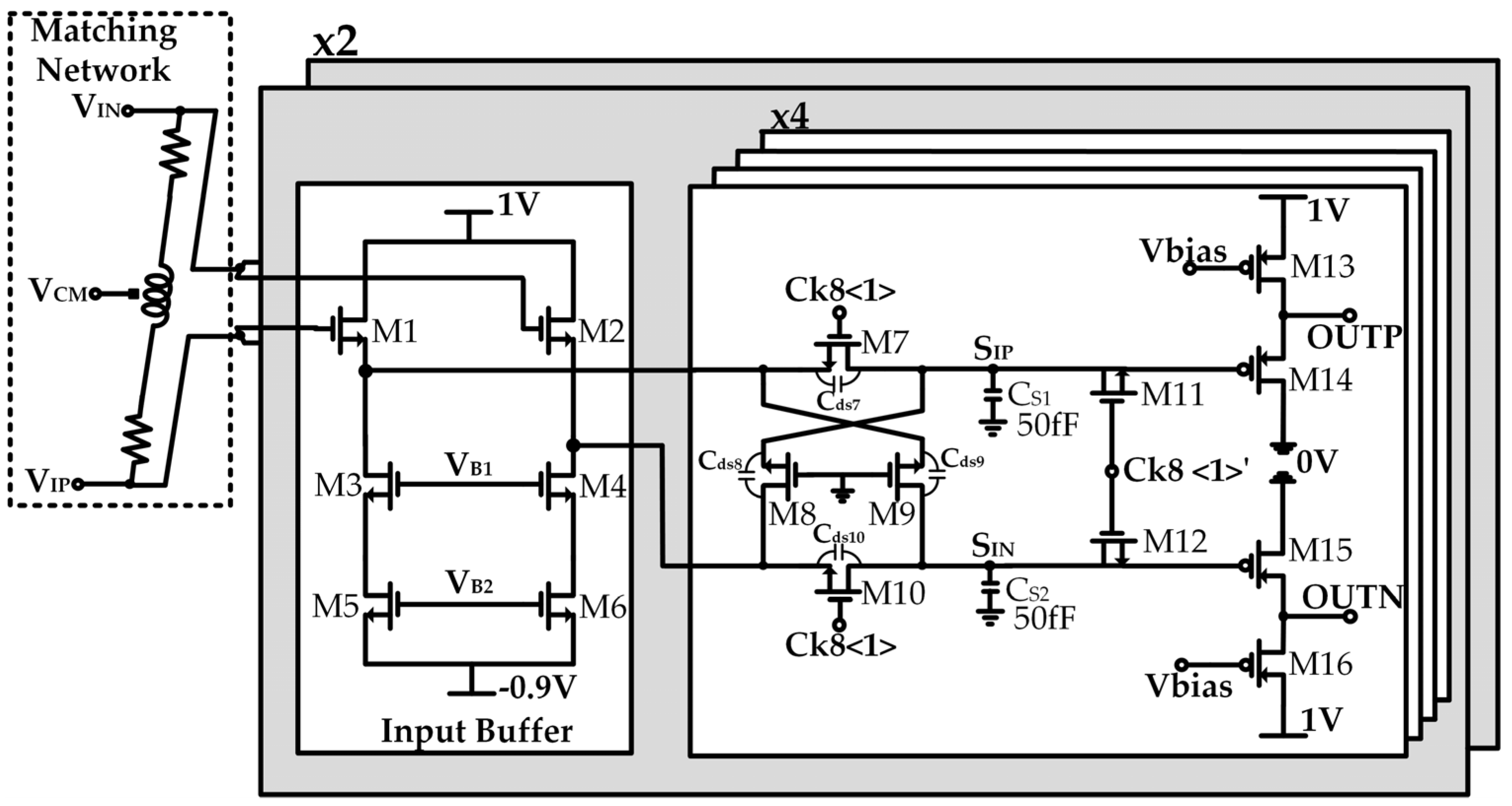
3.1. Sample Front-End

Figure 2 presents the schematic details of the sampling front-end (SFE), which contains a matching network, two input buffers that separately drive four slots of sampling stages. The differential input (VIP and VIN) signals are terminated by a matching network that consists of a pair of 50–Ω resisters and a T-coil with the center tap connected to a common voltage, VCM. The T-coil is employed to improve the input bandwidth of ADC by resonating the capacitances seen at the input. The input buffers are supplied by −0.9-V and 1.0 V voltages to generate a 200 mV common mode voltage to match the operation condition of the following T/Hs. In the sampling slots, a pair of NMOS transistors with two cross-coupled transistors are adopted to perform the sampling operation, where the sampled voltages can remain constant against the changing VIP and VIN when the sampling transistors are turned off. This is because the coupling voltages from the inputs VIP/VIN to SIP/SIN through Cds7 and Cds10 can be canceled by the coupling effect of Cds8 and Cds9. In order to eliminate the charge injection, transistors M11 and M12 are added to absorb the charges from the channel of M7 and M10. Each sampled voltage is applied to a source follower composed of PMOS transistors M13~M16 to drive the 8 SAR ADCs.

3.2. SAR ADC

Figure 3a shows the block diagram of the SAR ADC. It adopts 8 bit asynchronous SAR structure using a monotonous and split switching strategy with a 1 bit redundancy. An input signal is sampled by the top plates of all capacitors through the bootstrapped switch at the sampling phase. Here, the top plate sampling technology allows us to resolve the first bit without redistributing any charge, thus implementing N-bit data conversion with (N-1)-bit capacitor digital-to-analog converter (DAC). The issue of the common mode voltage change associated with the top plate sampling is addressed by a split switching strategy, where the bottom plates of half of the capacitors are connected to the Vref and the bottom plates of the other half of the capacitors are connected to the ground. This monotonous and split switching strategy can effectively reduce the power consumption. Meanwhile, we introduced a redundancy bit with a weight of 16 to relax the reference settling error to 11.7% (i.e., 16/136). This mainly benefits from the utilized top-sampling technique, where the first comparison involves no DAC settling process [20]. Driven by the asynchronous clock generator, the comparator sequentially produces the bit codes from MSB to LSB for each capacitor. Figure 3a shows the comparator that utilizes a double-tail structure and integrates an offset calibration block. This double-tail topology removes the static power, hence further improving the power efficiency. It is worthy to note that the offset calibration DAC is directly integrated into the comparator by tuning the operation fingers of the input pairs. This not only excludes the offset control DAC compared to the traditional designs [18,21], but also introduces no extra input noise. Figure 3b shows the details of the reference voltage generation circuit, which adopts the structure of the replica drive. The feedback loop provides high gain and stability, and the replica circuit adopts the open loop structure to meet the high-speed bandwidth requirements.

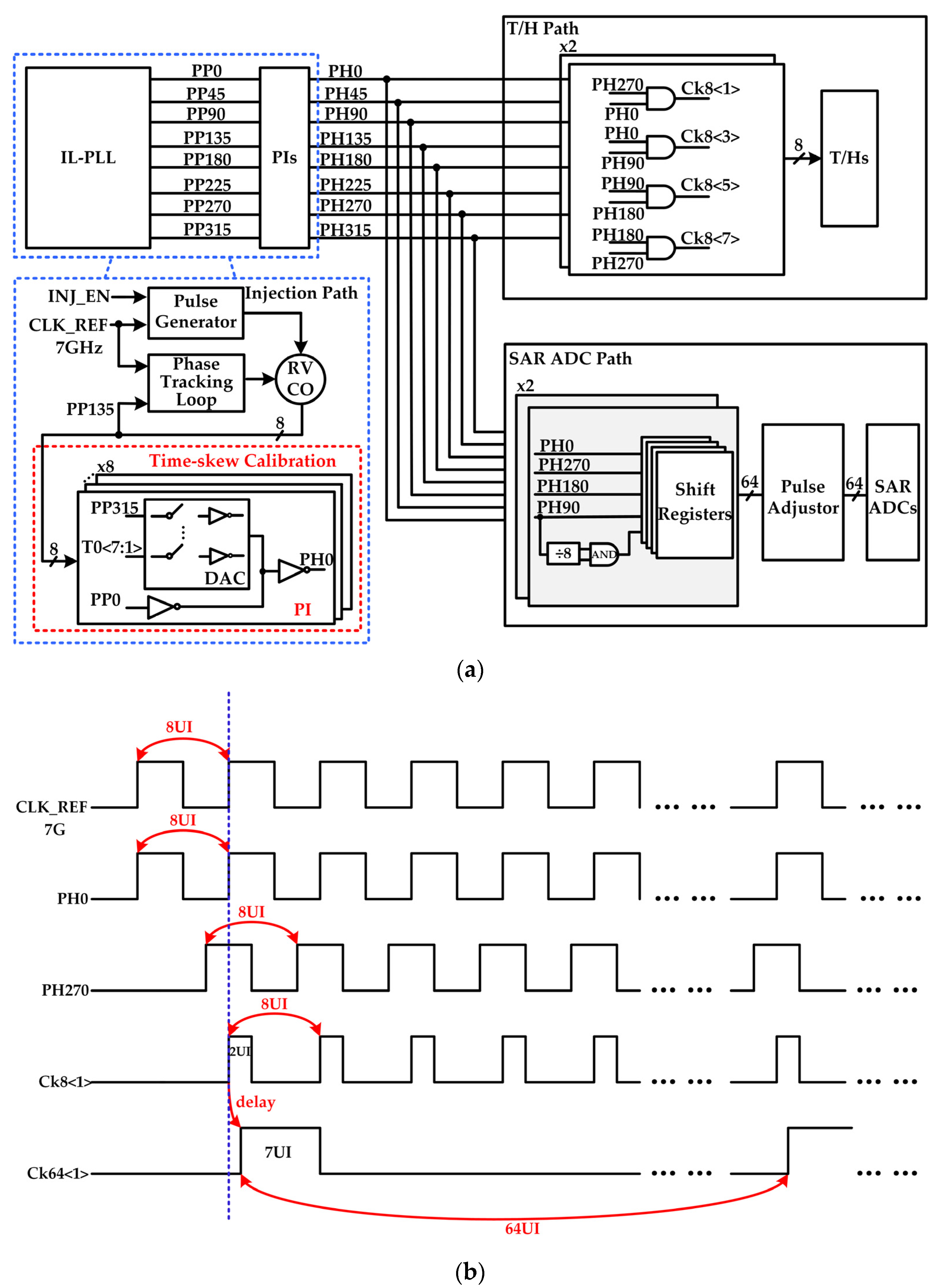
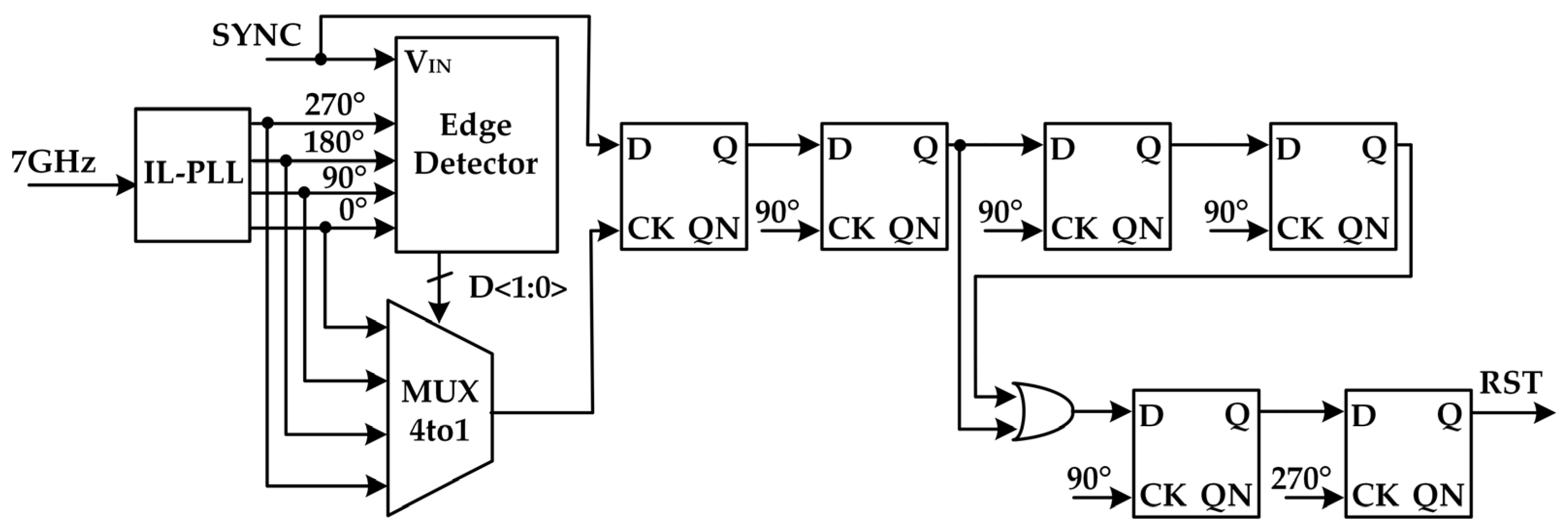
3.3. Multiple Phase Clock Generator

Figure 4a shows the block diagram of MPCG. It employs an RVCO-based IL-PLL reported in our previous work [22] to generate 8-phase 50% duty cycle 7 GHz clocks (i.e., PH0-45-90-135-180-225-270-315), where 8 partially rotating PIs are integrated to finely tune the phase spacing between these clocks. The skew-calibrated clocks are applied to the T/H path and SAR ADC path to generate 8-phase 7 GHz 25% duty cycle sampling pulses for sampling front-end and 64-phase 875 MHz sampling pulses for the SAR ADCs, respectively. By placing the RVCO close to the ANDing gates in the T/H path, the clock-driving path can be optimized to reduce the sampling jitter and power consumption. In the SAR ADC path, an 875 MHz clock with a 12.5% duty cycle is first generated by ANDing the two 135° spaced 1/8 rate clocks that are divided from PH90. This 12.5% clock is sequentially latched by the shift registers to generate the 64-phase sampling clocks for the SAR ADCs. To avoid the overlap between 64-phase 875 MHz, a pulse adjustor is proposed. The detail of the timing diagram is shown in Figure 4b; the unit interval (UI) is the period of sampling frequency. Figure 5 presents the schematic details of the developed pulse adjustor and its timing diagrams. As can be seen that the non-overlap time is determined by the time delay that is implemented by an inverter chain. Thanks to the multi-phase IL-PLL, the proposed clock scheme can directly generate an 8-phase 7 GHz 50% duty cycle clock. Additionally, it has a lower power consumption than the traditional high speed clock divider-based clock generation that needs CML logics to process the 28 GHz clock.

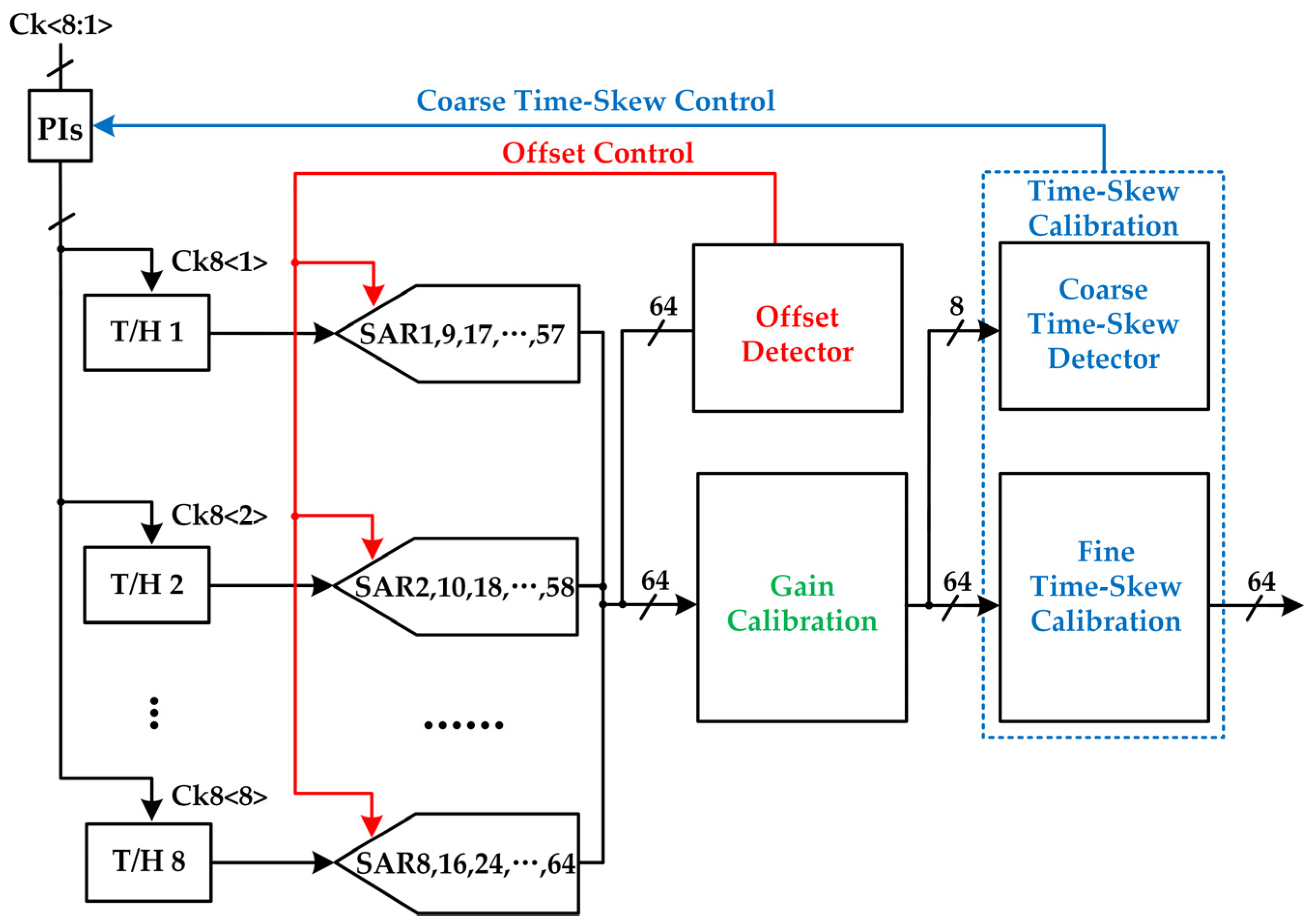
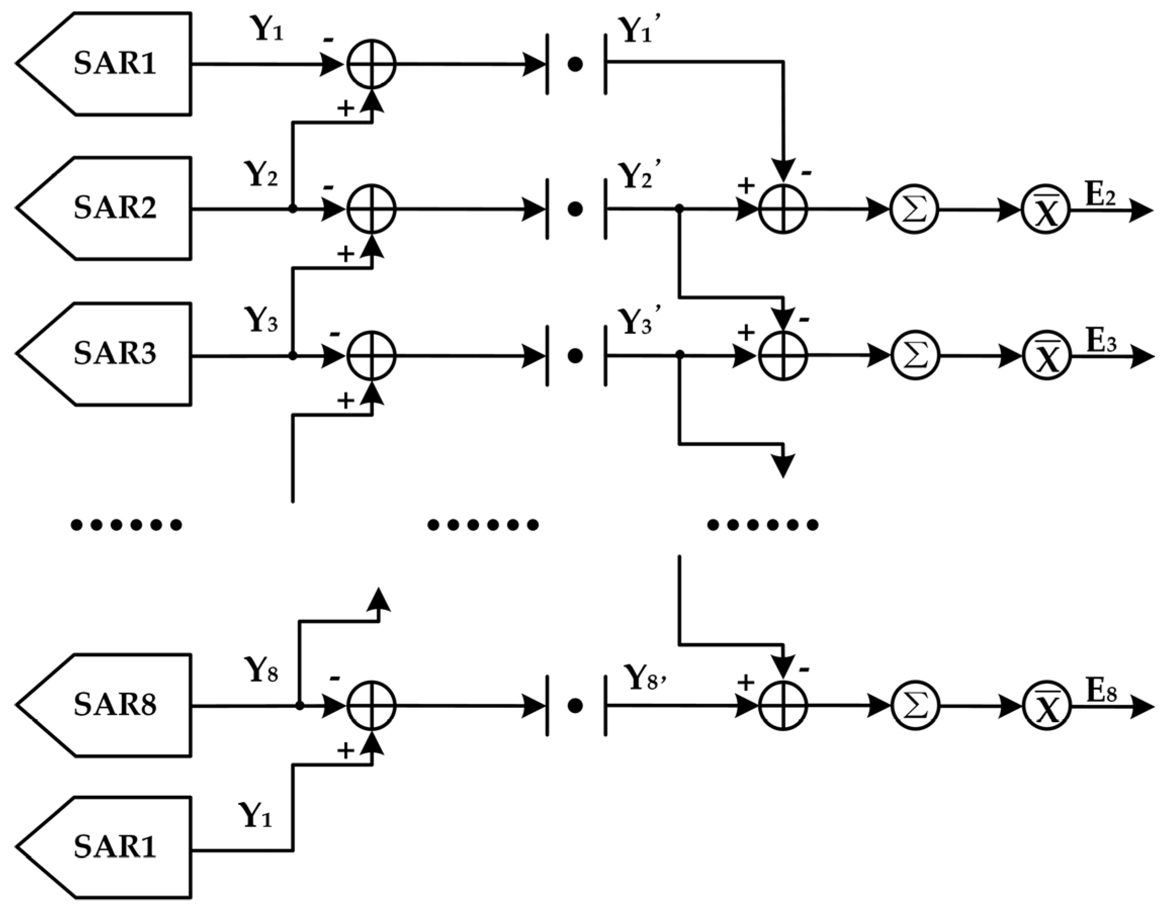
4. Dedicated Calibration

The performances of time-interleaved ADCs are limited by several impairments, including offset, gain, and time-skew mismatches [23,24,25]. To overcome these difficulties, we developed a dedicated calibration scheme, as shown in Figure 6. It contains an offset calibration loop, a coarse time-skew calibration loop, a gain calibration unit, and a fine time-skew calibration block. The offset errors are detected by the digital offset detector and corrected by the comparators located in the SAR ADC array. For the real-time gain error calibration, a traditional accumulation and averaging algorithm were implemented in the digital domain. The time-skew calibrations were divided into coarse and fine steps. The coarse time skews among the 8-way T/Hs were detected by the digital time-skew detector and adjusted by the PIs located at the sampling clock path (see Figure 4). The algorithm details of the coarse time-skew detector are shown in Figure 7, where the energy difference between the two adjacent SARs is computed to indicate the time skew that is supposed to be zero. Taking SAR2 as an example to explain the calibration process, the difference between Y2′ and Y1′ is taken as the instant energy difference, where Y2′ denotes the absolute difference between SAR3 and SAR2, and Y1′ represents the absolute difference between SAR2 and SAR1. The instant energy difference (Y2′-Y1′) was accumulated and averaged to produce a smooth time-skew control signal. The time-skew control signals for the other SARs were also calculated in the same way. When the calibration process reached stability, the accumulated energy difference between any two adjacent SARs approached to zero, hence the time skews between the 8-way samplings in the first stage were minimized. Additionally, a full-digital fractional delay filter (FDF) was utilized to further optimize the time skews among the total 64-way samplings. It is capable of realizing the individual delay adjustments for each SAR ADC. Figure 8 intuitively illustrates the operation principle of the FDF, where the interleaved 64-way SAR ADC outputs are fed to the finite impulse response (FIR) filter and the phase calculator. The FIR filter corrects the fine time skew using a group of proper coefficients. The phase calculator and the Lagrangian interpolator were adopted to calculate these coefficients; more specifically, the phase calculator first extracted the phase spacings between the reference channel (here, SAR1 is taken as the reference channel) and the other channels. By subtracting the ideal phase spacing, the phase errors can be computed, which are applied to the Lagrangian interpolator to estimate the FIR coefficient for each FIR tap, and hence finely calibrate the time-skew error. It is worth noting that this fractional delay filter-based fine calibration process highly relies on the real-time data output, which is implemented by the integrated 16-lane transmitters.

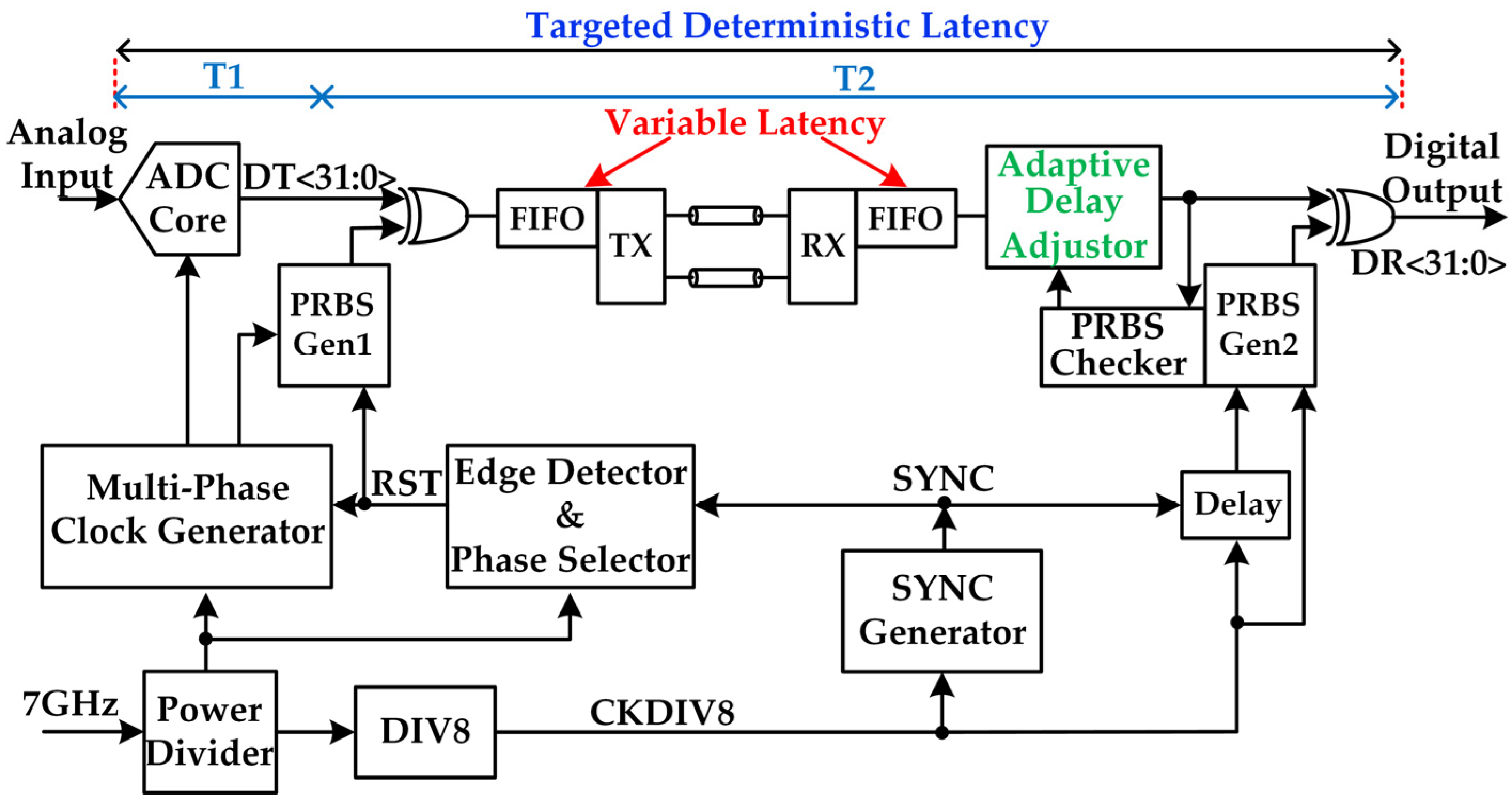
5. Deterministic Latency and Synchronization

The latency in the data conversion and transmission system refers to the delay from the sampling instance at the ADC to the far-end parallel output at the receiver. By implementing the deterministic latency, we can create a synchronized or interleaved sampling system across many ADCs in a single system. Nonetheless, it is not easy to realize a robust deterministic latency, which usually involves two issues: one is the phase uncertainty of the external synchronization signal with respect to the internal sampling clock that could cause a reset time competition; the other is the unfixed link delay resulting from a different channel length, bit recovery, and word align.
To overcome these difficulties, we proposed a precise synchronization mechanism. Figure 9 shows the simplified block diagram of the data conversion and transmission process from the ADC chip to receiver-side FPGA. The ADC chip is driven by an external 7 GHz clock, which is divided to generate CKDIV8 to drive the SYNC generator and receiver-side FPGA. This clocking scheme makes the link a synchronous system. As can be seen, the remaining time uncertainty of this link is mainly obtained from the reset time uncertainty, the FIFO before the transmitter, and the FIFO after the receiver and channel length variation. The reset time uncertainty could cause the ADC conversion latency T1 variation, and the other impairments are prone to change the data transmission latency T2. To make T1 a constant, we designed an edge detector and phase selector as shown in Figure 10, which can automatically detect the edge of SYNC and choose a proper sampling phase, hence preventing reset timing competition. Additionally, the sampled reset signal was aligned to a fixed 270 phase by a retiming chain, which ensured that the latency between the RST and the parallel output data of the ADC (i.e., T1) was a fixed value. To make the transmission latency T2 a constant, a common near-end data transmission position and far-end data collection instant with respect to SYNC were designated. Specifically, the data transmission starts immediately upon receiving SYNC, while the data collection starts after receiving SYNC with a dedicated delay. Here, the delay should cover the longest latency and its variation caused by the above-mentioned impairments. By sending and checking the previously defined PRBS patterns, the receiver can adaptively adjust the data delay (see Figure 9), hence making T2 a constant. Note that this delay adaption process only works in the initial PRBS sending and checking period. Once T1 and T2 are fixed, the whole latency from the input to the receiver-side parallel output is made deterministic.

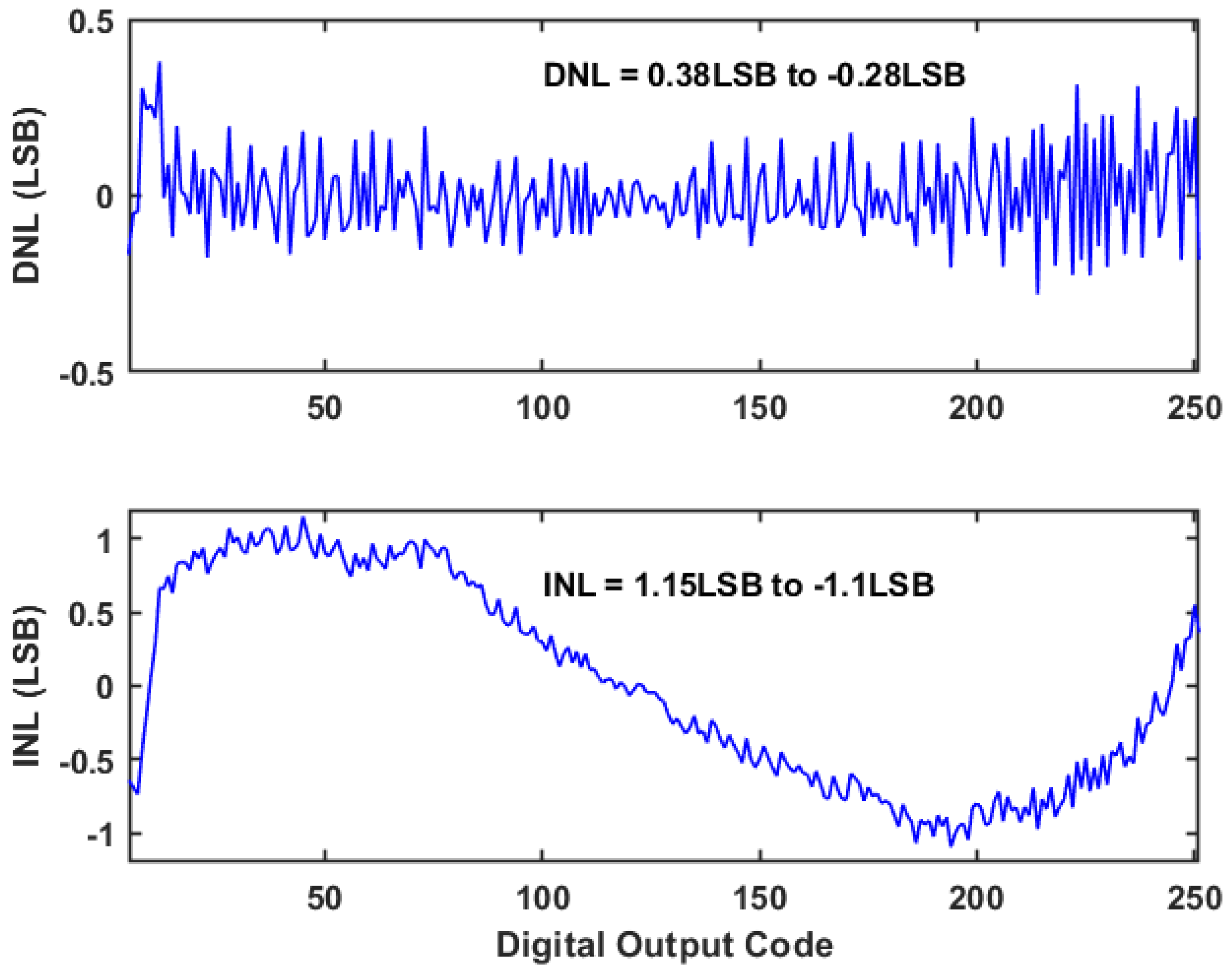
6. Measurement Results

The prototype TI-ADC was implemented in a 28 nm CMOS process and its chip micrograph is shown in Figure 11, where the ADC core occupies an active area of 1.2 mm × 1 mm. This prototype consumes a total power of 1.552 W, where the ADC core consumes 432 mW, the transmitters dissipate 1 W, and the digital engine consumes 120 mW. The fabricated ADC supports a differential input peak-to-peak voltage scale (600 mV). Figure 12 shows the measured DNL [26] and INL [26] at 56 GS/s with maximum values of +0.38/−0.28 LSB and +1.15/−1.1 LSB, respectively. Figure 13 presents the output spectrum where a 499.9 MHz input at 56 GS/s is shown after the gain and offset calibration. The SFDR [26] and SNDR [26] are 56.65 dB and 40.89 dB. Figure 14 further displays the measured spectrums with a 19.9 GHz input at 56 GS/s with the gain, offset and time-skew calibration, where the SFDR and SNDR achieve 40.68 dB and 36.38 dB. Figure 15 shows the measured SNDR versus the input frequencies at 56 GS/s with different calibration techniques. As can be observed, the SNDR can be significantly optimized by the gain and offset calibrations. Specifically, its value can be improved by at least 7 dB from 499.9 MHz to 19.9 GHz. The time-skew calibration shows a prominent improvement at high input frequencies, while exhibiting little effect on low input frequencies (<2 GHz). This can be explained by the fact that the sampling errors increase when the input frequency rises. The S11 measurement shows that it can achieve −20 dB at low frequencies and maintain around −10 dB at high frequencies. Table 1 summarizes the ADC performance comparison with the previously reported ADCs with similar resolutions and sampling rates. The ENOB of this work is 6.5 at a low-input frequency and 5.75 at a high-input frequency, which outperforms other designs [13,14,20,22]. The implemented ADC core only consumes 432 mW, resulting in a figure-of-merit of 85 fJ/conv. –step, which is much better than the other designs. The SFDR at la ow frequency is much higher than the other designs, indicating a high linearity of the overall data path. Another apparent feature of this ADC is its real-time output using 16-lane 28 Gb/s transmitters, which can bring in high convenience for practical applications, such as high-speed data collection and leading-edge instruments.

7. Conclusions

A real-time output 56 GS/s 8 bit SAR ADC integrated with 16-lane transmitters in a 28 nm CMOS is presented in the present study. The ADCs utilize an asynchronous technique, monotonous switching, split capacitors, and a 1 bit redundancy to achieve both a high-speed operation and low-power consumption. The developed RVCO-based IL-PLL is able to simultaneously generate the 8-phase sampling clock at 7 GHz, which not only alleviates the bandwidth requirement, but also reduces the power in contrast to traditional divider-based clock schemes. The calibration scheme consisting of offset, gain, and coarse–fine time-skew calibration techniques can effectively optimize the ADC performance. The proposed edge detector and phase selector can fix the ADC conversion latency, while the designed common near-end data transmission position and far-end data collection instant can determine the data transmission latency. The prototype ADC achieves an SNDR of 36.38 dB at 56 GS/s with a 19.9 GHz input frequency, outperforming other similar designs. The measurement results show that the developed calibration techniques can significantly optimize the SNDR, where the time-skew calibration shows a more apparent effect as the input frequency increases.

Author Contributions

J.L., X.Z. and D.W. designed the circuits, analyzed the measurement data, and wrote the manuscript. Y.Z. assisted with the circuit simulation and implementation. L.Z. and J.W. assisted with the chip package implementation and the PCB designing. L.W. performed the chip test and assisted with the chip measurement. X.L. provided some valuable guidance and confirmed the final version of the manuscript. All authors have read and agreed to the published version of the manuscript.

Funding

This research was supported by the Chinese Academy of Sciences Strategic Leading Science and Technology Project, no. XDC07020100 and the National Natural Science Foundation of China, no. 62074162.

Conflicts of Interest

The authors declare no conflict of interest.

References

  1. Upadhyaya, P.; Chi, F.; Lim, S.; Cho, J.; Chang, K. A Fully Adaptive 19–58-Gb/s PAM-4 and 9.5–29-Gb/s NRZ Wireline Transceiver with Configurable ADC in 16-nm FinFET. IEEE J. Solid-State Circuits 2019, 54, 18–28. [Google Scholar] [CrossRef]
  2. Krupnik, Y.; Perelman, Y.; Levin, I.; Sanhedrai, Y.; Eitan, Y.; Khairi, A.; Shifman, Y.; Landau, Y.; Virobnik, U.; Dolev, N.; et al. 112-Gb/s PAM4 ADC-Based SERDES Receiver with Resonant AFE for Long-Reach Channels. IEEE J. Solid-State Circuits 2020, 55, 1077–1085. [Google Scholar] [CrossRef]
  3. Lin, H.; Boecker, C.; Hossain, M.; Tangirala, S.; Vu, R.; Vamvakos, S.D.; Groen, E.; Li, S.; Choudhary, P.; Wang, N.; et al. ADC-DSP-Based 10-to-112-Gb/s Multi-Standard Receiver in 7-nm FinFET. IEEE J. Solid-State Circuits 2021, 56, 1265–1277. [Google Scholar] [CrossRef]
  4. Zheng, X.; Ding, H.; Zhao, F.; Wu, D.; Zhou, L.; Wu, J.; Lv, F.; Wang, J.; Liu, X. A 50–112-Gb/s PAM-4 Transmitter with a Fractional-Spaced FFE in 65-nm CMOS. IEEE J. Solid-State Circuits 2020, 55, 1864–1876. [Google Scholar] [CrossRef]
  5. Cai, C.; Zheng, X.; Chen, Y.; Wu, D.; Luan, J.; Zhou, L.; Wu, J.; Liu, X. A 1.4-Vppd 64-Gb/s PAM-4 Transmitter with 4-Tap Hybrid FFE Employing Fractionally-Spaced Pre-Emphasis and Baud-Spaced De-Emphasis in 28-nm CMOS. In Proceedings of the IEEE 47th European Solid State Circuits Conference (ESSCIRC), Grenoble, France, 13–22 September 2021; pp. 527–553. [Google Scholar]
  6. Cai, C.; Zheng, X.; Chen, Y.; Wu, D.; Luan, J.; Lu, D.; Zhou, L.; Wu, J.; Liu, X. A 1.55-to-32-Gb/s Four-Lane Transmitter with 3-Tap Feed Forward Equalizer and Shared PLL in 28-nm CMOS. Electronics 2021, 10, 1873. [Google Scholar] [CrossRef]
  7. Hong, H.; Kim, W.; Kang, H.; Park, S.; Choi, M.; Park, H.; Ryu, S. A decision-error-tolerant 45 nm CMOS 7b 1 GS/s nonbinary 2b/cycle SAR ADC. IEEE J. Solid-State Circuits 2014, 50, 543–555. [Google Scholar] [CrossRef]
  8. Ramkaj, A.; Strackx, M.; Steyaert, M.; Tavernier, F. A 1.25-GS/s 7-b SAR ADC with 36.4-dB SNDR at 5 GHz using switch-bootstrapping, USPC DAC and triple-tail comparator in 28-nm CMOS. IEEE J. Solid-State Circuits 2018, 53, 1889–1901. [Google Scholar] [CrossRef]
  9. Kull, L.; Toifl, T.; Schmatz, M.; Francese, P.A.; Menolfi, C.; Braendli, M.; Kossel, M.; Morf, T.; Andersen, T.M.; Leblebici, Y. A 3.1 mW 8b 1.2 GS/s single-channel asynchronous SAR ADC with alternate comparators for enhanced speed in 32 nm digital SOI CMOS. IEEE J. Solid-State Circuits 2013, 48, 3049–3058. [Google Scholar] [CrossRef]
  10. Wang, G.; Sun, K.; Zhang, Q.; Elahmadi, S.; Gui, P. A 43.6-dB SNDR 1-GS/s single-channel SAR ADC using coarse and fine comparators with background comparator offset calibration. In Proceedings of the 2017 IEEE European Solid State Circuits Conference (ESSCIRC), Leuven, Belgium, 11–14 September 2017; pp. 175–178. [Google Scholar]
  11. Schvan, P.; Bach, J.; Falt, C.; Flemke, P.; Gibbins, R.; Greshishchev, Y.; Ben-Hamida, N.; Pollex, D.; Sitch, J.; Wang, S.; et al. A 24 GS/s 6b ADC in 90nm CMOS. In Proceedings of the 2008 IEEE International Solid- State Circuits Conference (ISSCC), San Francisco, CA, USA, 3–7 February 2008; pp. 544–634. [Google Scholar]
  12. Duan, Y.; Alon, E. A 6b 46 GS/s ADC with >23 GHz BW and sparkle-code error correction. In Proceedings of the 2015 Symposium on VLSI Circuits (VLSI Circuits), Kyoto, Japan, 17–19 June 2015; pp. C162–C163. [Google Scholar]
  13. Kull, L.; Pliva, J.; Toifl, T.; Schmatz, M.; Francese, P.A.; Menolfi, C.; Brandli, M.; Kossel, M.; Morf, T.; Andersen, T.M. Implementation of low-power 6–8 b 30–90 GS/s time-interleaved ADCs with optimized input bandwidth in 32 nm CMOS. IEEE J. Solid-State Circuits 2016, 51, 636–648. [Google Scholar] [CrossRef]
  14. Xu, B.; Zhou, Y.; Chiu, Y. A 23-mW 24-GS/s 6-bit Voltage-Time Hybrid Time-Interleaved ADC in 28-nm CMOS. IEEE J. Solid-State Circuits 2017, 52, 1091–1100. [Google Scholar] [CrossRef]
  15. Jo, D.; Sung, B.; Seo, M.; Kim, W.; Ryu, S. A 40 nm CMOS 7 b 32 GS/s SAR ADC with background channel mismatch calibration. IEEE Trans. Circuits Syst. 2020, 67, 610–614. [Google Scholar] [CrossRef]
  16. Luan, J.; Wu, D.; Zheng, X.; Cai, C.; Wu, L.; Zhou, L.; Wu, J.; Liu, X. A Real-Time Output 50-GS/s 8-bit TI-ADC with Dedicated Calibration Techniques and Deterministic Latency. In Proceedings of the IEEE 47th European Solid State Circuits Conference (ESSCIRC), Grenoble, France, 13–22 September 2021; pp. 487–490. [Google Scholar]
  17. Greshishchev, Y.M.; Aguirre, J.; Besson, M.; Gibbins, R. A 40 GS/s 6b ADC in 65 nm CMOS. In Proceedings of the 2010 IEEE International Solid-State Circuits Conference (ISSCC), San Francisco, CA, USA, 7–11 February 2010; pp. 390–391. [Google Scholar]
  18. Kull, L.; Luu, D.; Menolfi, C.; Brndli, M.; Andrea, F.P.; Morf, T.; Kossel, M.; Cevrero, A.; Ozkaya, I.; Toifl, T. A 24–72 GS/s 8 b time-interleaved SAR ADC with 2.0-to-3.3 pJ/conversion and >30 dB SNDR at nyquist in 14 nm CMOS FinFET. IEEE J. Solid-State Circuits 2018, 53, 3508–3516. [Google Scholar] [CrossRef]
  19. Sun, K.; Wang, G.; Zhang, Q.; Elahmadi, S.; Gui, P. A 56 GS/s 8bit time-interleaved ADC with ENOB and BW enhancement techniques in 28 nm CMOS. IEEE J. Solid-State Circuits 2019, 54, 821–833. [Google Scholar] [CrossRef]
  20. Liu, C.; Chang, S.; Huang, G.; Lin, Y.; Huang, C.; Huang, C.; Bu, L.; Tsai, C. A 10b 100 MS/s 1.13 mW SAR ADC with binary-scaled error compensation. In Proceedings of the 2010 IEEE International Solid-State Circuits Conference (ISSCC), San Francisco, CA, USA, 7–11 February 2010; pp. 386–387. [Google Scholar]
  21. Cao, J.; Cui, D.; Nazemi, A.; He, T.; Li, G.; Catli, G.; Catli, B.; Khanpour, M.; Hu, K.; Ali, T.; et al. A transmitter and receiver for 100Gb/s coherent networks with integrated 4 × 64 GS/s 8b ADCs and DACs in 20 nm CMOS. In Proceedings of the 2017 IEEE International Solid-State Circuits Conference (ISSCC), San Francisco, CA, USA, 5–9 February 2017; pp. 484–485. [Google Scholar]
  22. Zheng, X.; Lv, F.; Zhou, L.; Wu, D.; Wu, J.; Zhang, C.; Rhee, W.; Liu, X. Frequency-Domain Modeling and Analysis of Injection-Locked Oscillators. IEEE J. Solid-State Circuits 2020, 55, 1651–1664. [Google Scholar] [CrossRef]
  23. Razavi, B. Design consideration for interleaved ADC. IEEE J. Solid-State Circuits 2013, 48, 1806–1817. [Google Scholar] [CrossRef] [Green Version]
  24. Lee, S.; Chandrakasan, A.; Lee, H. A 1 GS/s 10b 18.9 mW Time-Interleaved SAR ADC with Background Timing Skew Calibration. IEEE J. Solid-State Circuits 2014, 49, 2846–2856. [Google Scholar] [CrossRef]
  25. Chen, V.; Pileggi, L. A 69.5 mW 20 GS/s 6b time-interleaved ADC with embedded time-to-digital calibration in 32 nm CMOS SOI. IEEE J. Solid-State Circuits 2014, 49, 2891–2901. [Google Scholar] [CrossRef]
  26. Maloberti, F. Data Converters; Springer Science & Business Media: Berlin, Germany, 2007. [Google Scholar]
Figure 1. Overall architecture of the proposed 56 GS/s time-interleaved ADC.
Electronics 11 00688 g001
Figure 2. The ADC sampling front-end.
Electronics 11 00688 g002
Figure 3. (a) SAR ADC details. (b) Reference voltage generation circuit.
Electronics 11 00688 g003
Figure 4. (a) Multiple phase clock generator. (b) The timing diagram.
Electronics 11 00688 g004
Figure 5. The proposed pulse adjustor.
Electronics 11 00688 g005
Figure 6. Overall calibration diagram.
Electronics 11 00688 g006
Figure 7. Coarse time-skew detector.
Electronics 11 00688 g007
Figure 8. Fine time-skew detector.
Electronics 11 00688 g008
Figure 9. Deterministic latency and synchronization diagram.
Electronics 11 00688 g009
Figure 10. Edge detector and phase selector.
Electronics 11 00688 g010
Figure 11. (a) Chip micrograph. (b) Power breakdown.
Electronics 11 00688 g011
Figure 12. Measured INL and DNL.
Electronics 11 00688 g012
Figure 13. Measured output spectrum when the input frequency is 499.9 MHz at a 56 GS/s sampling rate.
Electronics 11 00688 g013
Figure 14. Measured output spectrum when the input frequency is 19.9 GHz at a 56 GS/s sampling rate.
Electronics 11 00688 g014
Figure 15. Measured SNDR versus input frequency at a 56 GS/s sampling rate.
Electronics 11 00688 g015
Table 1. Performance summary and comparison.
Specification[12][13][19][21]This Work
Technology (nm)2832282028
Resolution (bits)68888
Sampling Rate (GS/s)4690566456
Output CommunicationMemory On-chipMemory On-chipMemory On-chipIP IntegrationReal-time Output
SNDR@fin,low (dB@GHz)27@1236@640.5@737.6@8[email protected]
SNDR@fin,high (dB@GHz)[email protected][email protected]33@2733.7@16[email protected]
SFDR@fin,low (dB@GHz)[email protected]NA47.7@250@1[email protected]
SFDR@fin,high (dB@GHz)[email protected][email protected]42@27[email protected][email protected]
Power (mW)381667702950432
FOM (fJ/conv.-step)45314414524085
Area (mm2)0.14 (active)0.45 (active)0.878 (active)1.771.2 (active)
Publisher’s Note: MDPI stays neutral with regard to jurisdictional claims in published maps and institutional affiliations.

