Article

A Broad Dual-Band Bandpass Filter Design Based on Double-Layered Spoof Surface Plasmon Polaritons

1
College of Electronic and Information Engineering, Nanjing University of Aeronautics and Astronautics, Nanjing 210016, China
2
College of Electric Power Engineering, Nanjing Institute of Technology, Nanjing 211167, China
3
College of Electronics and Information, Jiangsu University of Science and Technology, Nanjing 212003, China
*
Author to whom correspondence should be addressed.
Electronics 2022, 11(5), 697; https://doi.org/10.3390/electronics11050697
Submission received: 6 December 2021 / Revised: 7 February 2022 / Accepted: 16 February 2022 / Published: 24 February 2022
(This article belongs to the Section Microwave and Wireless Communications)

Abstract

:
In this work, a broad dual-band bandpass filter is designed by applying double-layered spoof surface plasmon polaritons (DLSSPPs) as the main transmission line (MTL) and loading combined-stub dual-mode resonators (CSDMRs) onto the MTL with certain spaces. Each CSDMR consists of an open stub and a short stub that are connected in parallel. Efficient mode conversion between the quasi-transverse electromagnetic waves in the microstrip line and the spoof surface plasmon polaritons (SSPPs) on the double-layered surface plasmon waveguide is realized using gradient double-layered metal gratings and via the sector structure impedance matching technique. A parametric study of the CSDMR demonstrates that center frequencies and bandwidths can be controlled by varying the stub lengths and widths of the CSDMRs. A second-order dual-band filter is designed and fabricated, and simulated and experimental S-parameters agree well. A lower loss of the passband is achieved compared with the filters that apply single-layered SSPPs. The space between two CSDMRs is shortened because of the slow-wave effect of the DLSSPPs. The lowpass performance of the DLSSPPs exhibits good rejection from the cutoff frequency above.

1. Introduction

Surface plasmon polaritons (SPPs) are surface electromagnetic waves that propagate along the interface between two materials with opposite permittivity and whose electromagnetic fields exponentially decay in the transverse direction [1]. SPPs have a broad range of applications at visible and near-infrared wavelengths. However, SPPs cannot exist when the frequency is reduced to the microwave or terahertz wavelength bands, because metals behave like perfect electric conductors [2,3].
The use of ultrathin corrugated metallic strips has been proposed to propagate SSPPs on planar paths; doing so may achieve plasmonic functional integrated circuits at microwave and terahertz frequencies [4,5,6,7]. SSPPs are electromagnetic surfaces constrained by slots or holes on a metal surface and propagate on the periodic surface of the metal surface wave. SSPPs can overcome the diffraction limit owing to their ability to confine electromagnetic fields in a deep subwavelength scale with high intensity [8,9,10]. Several studies have reported that SSPPs can be excited in textured structures with periodic subwavelength grooves, holes, and dimmers [11,12,13,14,15,16,17]. Various devices based on SSPPs have been developed for applications in optoelectronics, photovoltaics, and nanophotonics [18,19,20,21,22]. Importantly, the propagation characteristics of SSPPs can be well satisfied by designing suitable geometric parameters.
As essential microwave devices, bandpass filters have been designed on the basis of various forms of SSPPs, such as hybrid substrate integrated waveguides (HSIWs) [23], quasi-SSPPs (QSSPPs) [24], substrate integrated plasmonic waveguides (SIPWs) [25], and multistage SSPPs coupled to resonators [26,27]. A highly efficient conversion from conventional guided waves to SPPs is achieved in the broadband by using ultrathin corrugated metallic strips with a transition with gradient grooves. Using such strips allows the realization of combined devices and circuits of guided waves and SSPPs, especially surface plasmonic bandpass filters with SSPP structures [28,29,30,31,32,33,34,35]. Electromagnetic waves can also be tightly confined within metallic gratings to achieve a low radiation loss. Compared with the single-layered spoof surface plasmon waveguide (SLSSPW), the double-layered spoof surface plasmon waveguide (DLSSPPW) performs better in designing low-loss structures.
In this work, a broad dual-band bandpass filter based on DLSSPPs is constructed by loading two combined-stub dual-mode resonators (CSDMRs) onto the SSPP main line with a certain distance. Several good features are obtained by this structure. First, thanks to the tight confinement of electromagnetic waves between metal layers, a relatively lower loss can be achieved with DLSSPPs than with solutions based on single-layered SSPPs (SLSSPPs). Second, a relatively shorter filter length can be obtained owing to the slow-wave effect introduced by the SSPPs when compared with microstrip-form stub filters. Third, the filter has a good harmonic rejection above the cutoff frequency of the DLSSPPs due to the lowpass response of the DLSSPPs. Fourth, the center frequencies and bandwidths can be controlled by varying the parameters of the CSDMRs.

2. Materials and Methods

The proposed DLSSPPs has a comb shape (Figure 1a). In the figure, length of the cell structure, groove depth, groove width, and strip width are denoted by D, G, S, and W, respectively. In the microwave and terahertz frequencies, the metal can be reasonably assumed as a perfect electric conductor. The dispersion curves of transverse magnetic polarized waves propagating in the x direction along the DLSSPPs were analyzed, and only the fundamental mode was considered. The geometrical parameters D = 6 mm, S = 2 mm, and W = 2 mm and groove depth G with four values (1, 2, 3, and 4 mm) were selected for inducing the SSPPs to propagate in the microwave and terahertz frequencies. As shown in Figure 1b, the dispersion relations of the double-layered metal gratings were obtained from the eigenmode solver of the commercial software CST Microwave Studio, in which the dielectric substrate was selected as F4B. It had a relative dielectric constant εr = 2.65 and a loss angle tangent tan δ = 0.003, and the thickness was chosen to be H = 1 mm. The simulated dispersion relationships with different groove depths G were obtained, as shown in Figure 1b. In the figure, the dashed black line is the curve for the light line in free space, and the solid lines correspond to groove depths ranging from 1 mm to 4 mm.
As groove depth G increases, the dispersion curve further deviates from the dashed light line, and the cutoff frequency decreases. Thus, the coplanar waveguide and double-layered SSPPs have a mismatch of momentum, especially at the equivalent asymptotic frequency. Hence, exciting the DLSSPPs propagating on this surface plasmon waveguide efficiently with coplanar input/output ports is difficult. For momentum matching and mode conversion, a double-layered circuit transition (region II of Figure 2) was constructed using the comb-shaped SSPPs with groove depths gradually changing from 0 (CPW) to G with equal step. For better impedance matching, two sector structures were placed at the two sides to provide a flaring ground to realize smooth impedance matching.
The structures containing CPW sections, mode transition sections, and DLSSPP sections, which are regions I, II, and III, respectively, are presented in Figure 2a. CPW has the parameters of W0 = 0.34 mm and W1 = 2 mm. The flaring curves of the sectors in region II can be described as y = C 1 e a x + C 2 with a = 0.15 , C 1 = y 2 y 1 e a x 2 e a x 1 , and C 2 = y 1 e a x 2 y 2 e a x 1 e a x 2 e a x 1 , with p1 = (x1, y1) and p2 = (x2, y2) being the start and end points of the curve, respectively (x1 = 0, y1 = 0, x2 = 40 mm, y2 = 20 mm). The groove depth of the gradient DLSSPPW increases from 0.8 mm to 3.2 mm (d0 to d3) with an equal step, thereby realizing a smooth transition of momentum.
Region III is the main section of the SSPPs, as illustrated in Figure 2a, in which the period, groove depth, and grove width of the SSPPs are chosen as D = 6 mm, G = 4 mm, and S = 2 mm. According to Figure 1b, the cutoff frequency is approximately 9 GHz, which is the asymptotic frequency of the dispersive curve [35].
The performance of the structure was further quantitatively evaluated by also simulating it with the commercial EM software CST by using the S parameters shown in Figure 3. S11 is almost less than −10 dB within the frequency range of 0.5 GHz to 8 GHz, indicating that good mode transition and momentum matching are achieved. S21 verifies that the proposed structure has excellent lowpass filtering characteristics, and 30 dB suppression is obtained at ≥9 GHz.
The basic topology of a microwave bandpass filter contains N resonators and N + 1 J inverters [36], as shown in Figure 4. If it is a dual-band bandpass filter (DBBF) with center frequencies of f1 and f2, the J inverters should be dual-mode J inverters, and the resonators should be dual-mode resonators, working at the two center frequencies of f1 and f2.
Several units of DLSSPPs with a total electrical length of approximately 90° are used as J inverters in realizing the single-band bandpass filter [35]. For the dual-band bandpass filter design, an approximate realization of a dual-mode J inverter may be a section of the DLSSPW with a 90° electrical length at a frequency of (f1 + f2)/2. The J values of the dual-mode J inverter will be the equivalent characteristic admittances of the DLSSPW at the center frequencies.
After the J inverters are determined, the susceptance slopes of the dual-mode resonators at each passband can be computed [36], and the susceptance slopes are inversely proportional to the bandwidths.
In this study, a dual-mode resonator can be realized with a CSDMR that contains parallel-connected open- and short-circuited stubs, as shown in Figure 5. Looking into the connecting point, the input admittance can be given as
Y i n = j B i n ( f ) = j ( tan θ 2 ( f ) Z 2 cot θ 1 ( f ) Z 1 )
Here, we have the electrical lengths: θ i ( f ) = 2 π L i λ g = ω L i c ε e   i = 1 , 2 and λ g is the guided wavelength.
The resonances occur at the frequencies where the input admittance is zero. At each resonance, the CSDMR can be equalized to a parallel LC resonator, as shown in Figure 5. We have the transcendental equation below.
tan θ 1 ( f ) tan θ 2 ( f ) = Z 2 / Z 1
The lowest two roots of Equation (2) are the two resonant frequencies of the CSDMR. We may know that the frequencies will decrease if the physical lengths L1 and L2 are increased. Moreover, the frequency ratio f1/f2 is dominated by the physical length ratio L1/L2 and the characteristic impedance ratio Z1/Z2.
According to Foster’s reactance theorem, between every two susceptance zeros of a CSDMR, there will be a susceptance pole, and a transmission zero will be introduced if the CSDMR is loaded on the DLSSPP MTL. The TZs can be introduced by the open stub or the short stub of the CSDMR, and the open-stub TZs (fTZo) and short-stub TZs (fTZs) can be given as follows:
f T Z o = 2 n + 1 4 c ε e L 2 n = 0 ,   1 ,   2   f T Z s = n 2 c ε e L 1 n = 0 ,   1 ,   2  
According to Equation (3), the first TZ will be introduced by the short stub and be located at DC. The second TZ produced by the open stub will be located between the first and second passbands if the two stubs have similar lengths. The third TZ given by the short stub will be above the second passband.
If the resonating frequencies f1 and f2 are determined, then we can compute the susceptance slopes as follows:
b i ( f ) = B i n ( f ) ω = L 1 csc 2 θ 1 Z 1 c ε e + L 2 sec 2 θ 2 Z 2 c ε e = 1 Z 1 c ε e ( L 1 csc 2 θ 1 + L 2 sec 2 θ 2 Z 2 / Z 1 ) , i = 1 , 2
The susceptance slopes, b1 and b2, are mainly dominated by the characteristic impedances, Z1 and Z2. When Z1 and Z2 increase without changing Z2/Z1, b1 and b2 decrease inversely, and the bandwidths of the two passbands are expended. In theory, the parameters of each dual-mode resonator should be tuned or optimized for achieving the required center frequencies and susceptance slopes, according to the specified two passbands.
However, the theoretical design of a dual-band bandpass filter will not be fully applicable, owing to practical limitations. The dual-mode J inverters are not ideal, because the electric length is not 90° at f1 and f2, and this will incur unpredictable deviations in the center frequencies and susceptance slopes for each dual-mode resonator. Moreover, unlike TEM transmission lines, the DLSSPPs can be regarded as frequency-dispersion transmission lines, that is, the phase velocity varies with the frequency. Furthermore, as the TZs are close to the passbands, the positions of TZs exert important effects on the center frequencies and bandwidths.
In practical design, a parametric study of dual-band bandpass filters with the help of electromagnetic simulation can be conducted for achieving required center frequencies and bandwidths.

3. Structure and Parametric Study

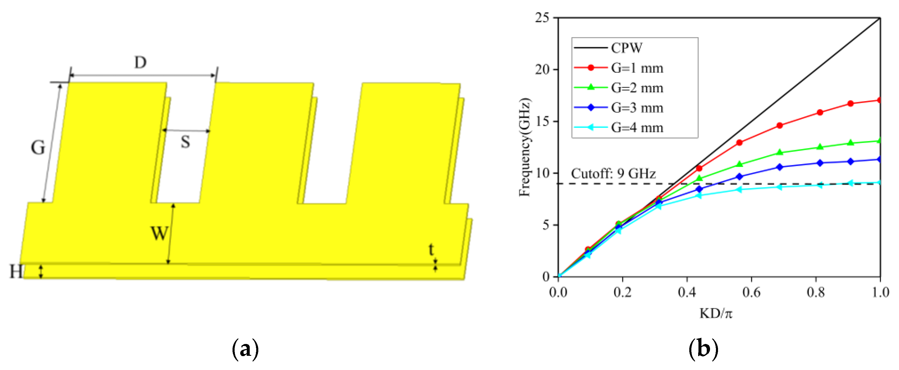
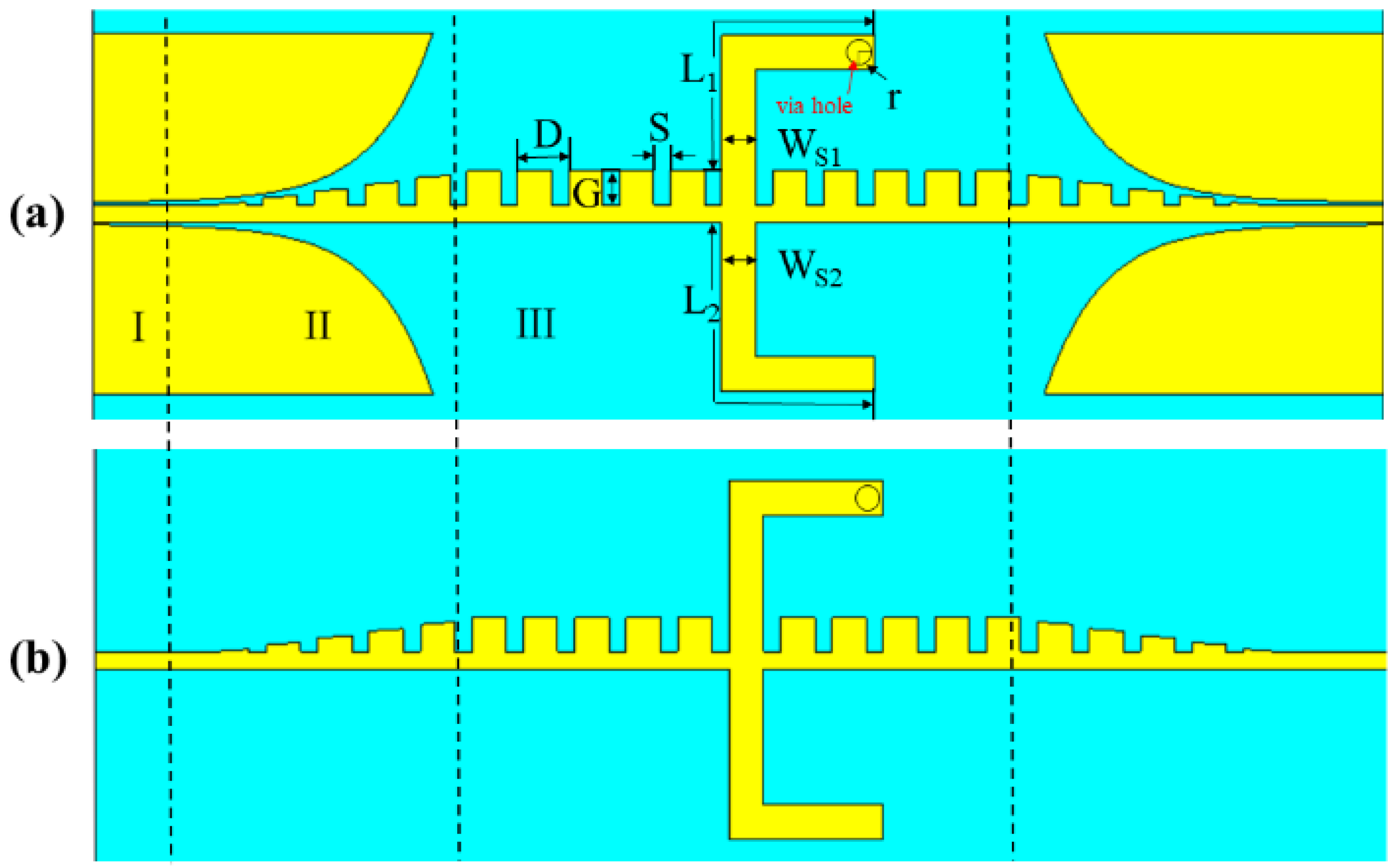
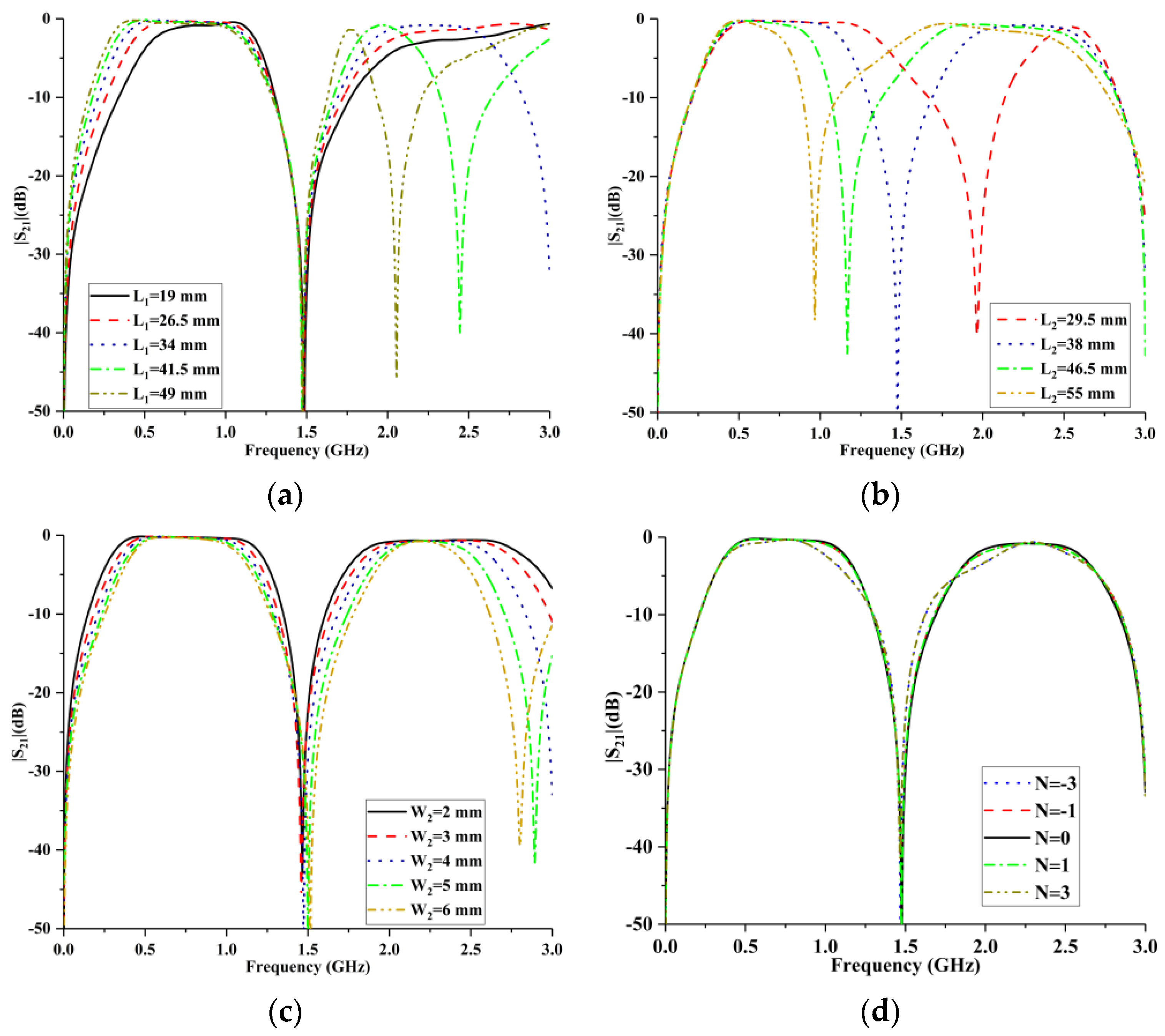
3.1. Structure and Parametric Study of DLSSPW Loaded with a Single CSDMR

A first-order dual-band bandpass filter is given in Figure 6. A CSDMR is loaded on the DLSSPW mainline, and the open- and short-stubs are on the two sides of the mainline. The dimensions of the dual-band bandpass filter are minimized by bending each of the two stubs in an “L” shape. We may extract a 90° section of the DLSSPW on each side of the CSDMR as a J inverter. A parametric study of the filter was conducted by carrying out S-parameter simulations with commercial EM software CST.
In Figure 7, we give some S parameter responses of a first-order dual-band bandpass filter, when different parameters vary. We can observe transmission zeros at DC between the passbands and above the second passband. These TZs are all produced by the open stub of the CSDMR.
Figure 7a,b illustrate that the center frequencies of the two passbands are decreasing when either L1 or L2 is increasing. When L1 is increased, the first passband is expanded, and the second passband is narrowed. By contrast, when L2 is increased, the first passband is narrowed, and the second passband is broadened. Figure 7c depicts that the two bandwidths increase simultaneously when the widths of the open- and short- stubs are increased because the characteristic impedances of Z1 and Z2 decrease. N is the number of comb-shape structures between the “L” shape structure and the center comb shape structure, and negative and positive numbers represent the left and right sides of the center comb shape structure, respectively. As shown in Figure 7d, at the same distance from the center comb shape structure, the center frequency and bandwidth of the two passbands are equal. The farther away from the center comb shape structure, the center frequency remains unchanged and the bandwidth decreases.

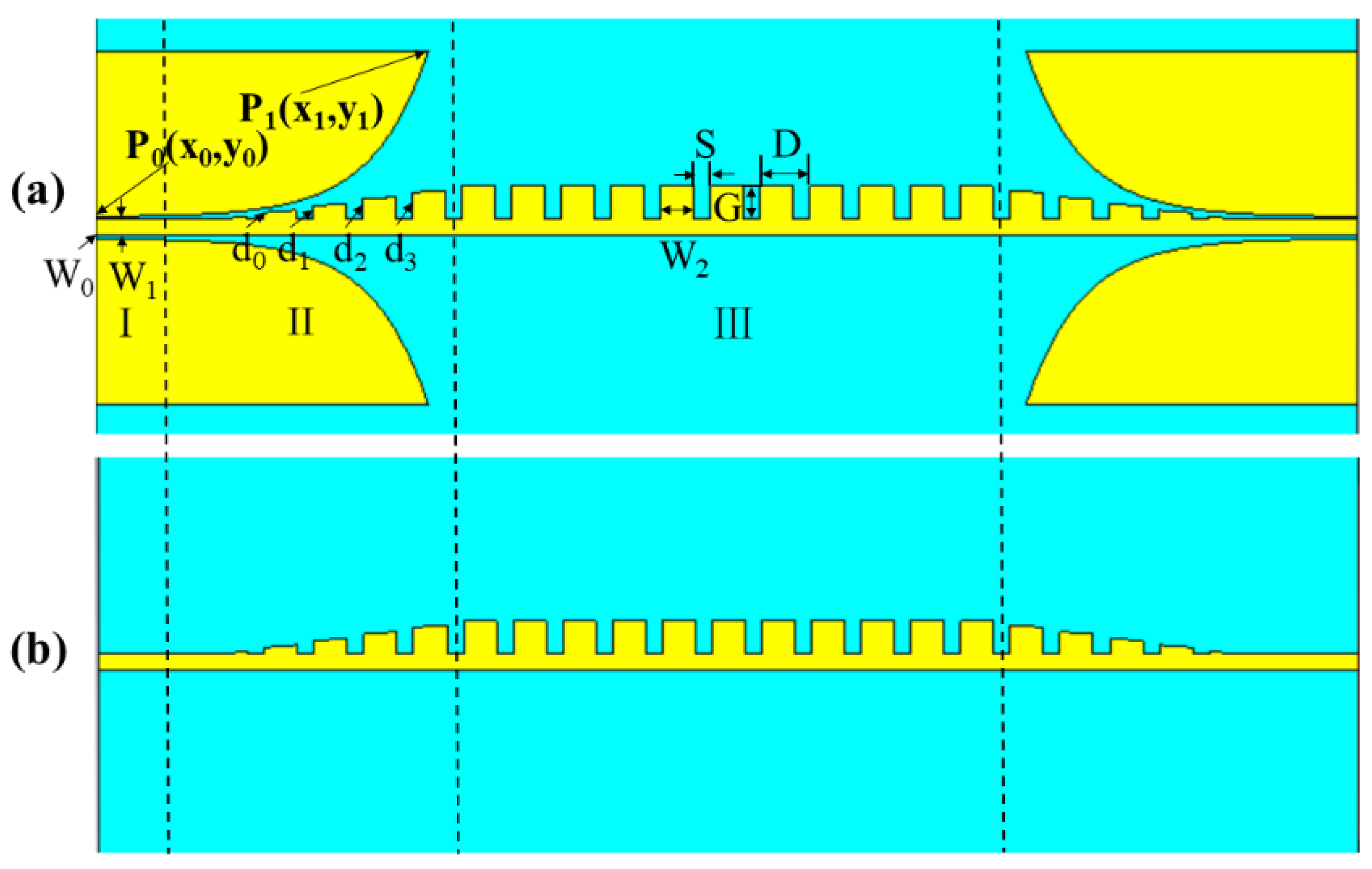
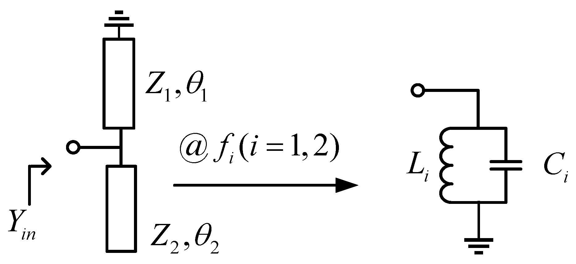
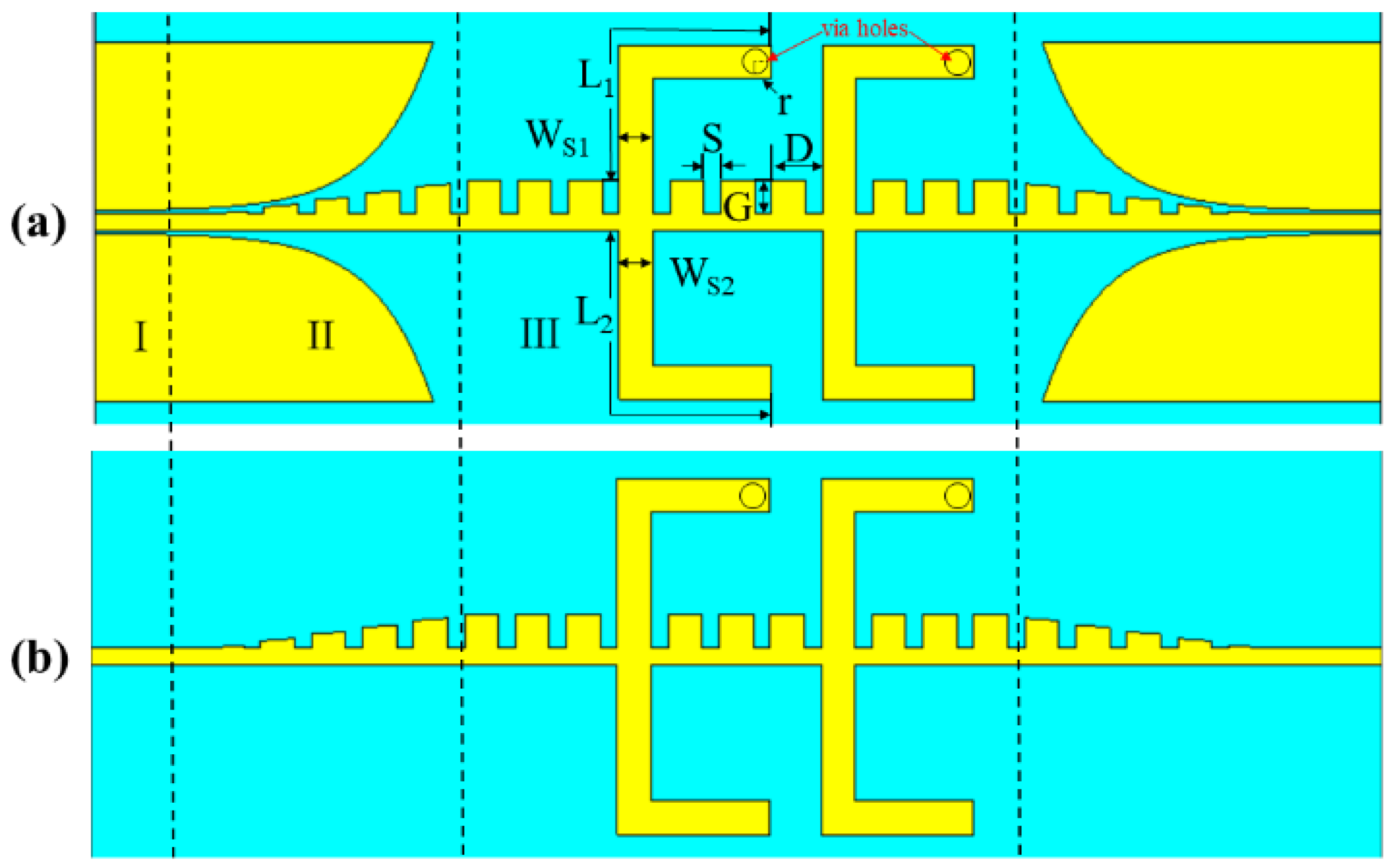
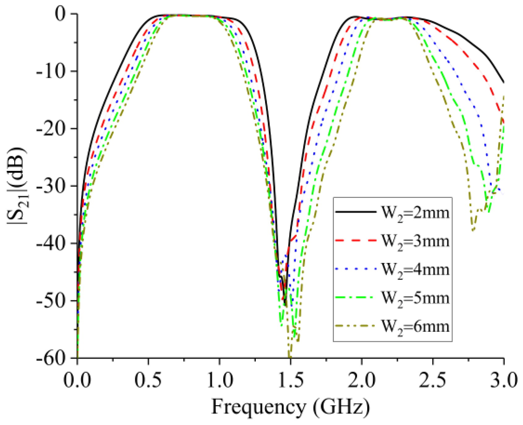
3.2. Structure of a Second-Order Dual-Band Bandpass Filter and Simulation Results

For higher out-of-band rejection, a second-order dual-band filter was designed by loading two CSDMRs with the same dimensions on the DLSSPW (Figure 8). The distance between the two CSDMRs needs to be a quarter wavelength at the frequency of (f1 + f2)/2. Due to the slow-wave effect, the guided wavelength of the DLSSPW becomes smaller than those of the microstrip line and the coplanar waveguide, leading to a shorter distance between two CSDMRs. In the case that f1 and f2 are 0.8 GHz and 2.2 GHz, four DLSSPP units with a length of 22 mm are used for connecting two CSDMRs, while the length is about 33% shorter than a corresponding quarter-wavelength microstrip line.
The simulated S21 of the second-order dual-band bandpass filter with different W2 is given in Figure 9. When W2 increases, the center frequencies basically remain unchanged, and the bandpass bandwidths gradually become narrower. The isolation between the passbands is increased along with the filter order. As two CSDMRs are loaded, we can observe two closely distributed transmission zeros and greatly increased isolation between the two passbands.

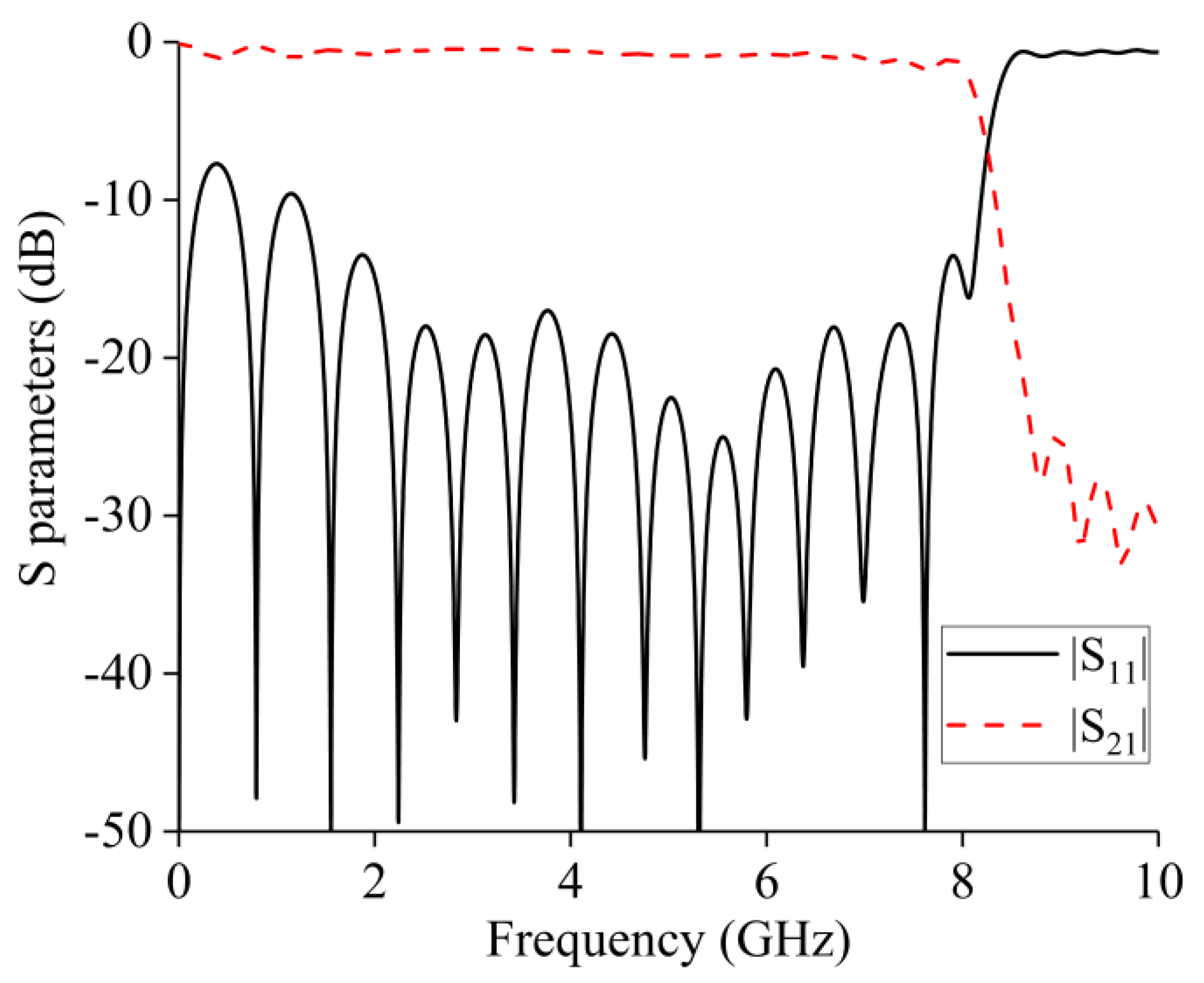
4. Results and Discussion

The proposed structure of the DLSSPW dual-band bandpass filter is validated. A second-order prototype filter with the dimensions of L1 = 34 mm, L2 = 38 mm, and W2 = 4 mm was fabricated (Figure 8). The same substrate with εr = 2.65 and height H = 1 mm was used, and the same transition circuit with the same dimension was adopted.
The simulation and measurement results are presented in Figure 10. The results are in good agreement. A dual-band bandpass response within the frequency ranges of 0.5 GHz to 2.5 GHz, which is below the cutoff frequency of the DLSSPW, can be observed. The two passbands range from 0.5 GHz to 1.1 GHz and from 2 GHz to 2.4 GHz. The measured return losses (RLes) of the lower and upper passbands are 15 and 14 dB, respectively. The lowest measured insertion losses (ILes) within the passbands are 2 and 2.5 dB, which are a bit larger than the simulated results. Two transmission zeros can be observed between the two passbands, thereby increasing the isolation between the two passbands. The deviations in ILes and passband frequencies observed are mainly caused by the fabrication tolerances and the error of dielectric constant of the substrate. The two side connectors also add to the IL.
The filtering response of the DLSSPW-based dual-band bandpass filter was further investigated. The field distribution at five frequencies both inside and outside of the passbands is given in Figure 11. At 0.1, 1.4, and 2.8 GHz (which are within the stopbands), the electric field can be hardly excited and transmitted from one port to another. By contrast, at 0.8 and 2.1 GHz, the field can be efficiently excited and fully transmitted to the other port. The total dimension of the circuit is 152 mm × 42 mm (0.76 λg × 0.21 λg). A photograph of the fabricated second-order dual-band bandpass filter is provided in Figure 12.
The performances of the filter developed herein was compared with those of other published SSPP-based filter designs (Table 1). Among all the filters, only this design has a dual-band bandpass filter with broad bandwidths. Owing to the tight confinement of electromagnetic waves between the two layers, the radiation loss of DLSSPPs is much lower than those of SLSSPPs. This also produces smaller ILes and flatter passbands than those filters using SLSSPPs. Moreover, the two-layer structure makes realizing short/open stubs and CSDMR possible, leading to dual-band bandpass responses and full control of the center frequencies and bandwidths. The measured functional bandwidth (FBW) can be given as
F B W = f 2 f 1 ( f 2 + f 1 ) / 2
Here, the operating frequency bandwidth of the filters from Table 1 is from f1 to f2.

5. Conclusions

Double-layered SSPPs with comb-shape units are used for the main transmission line to realize broad dual-band bandpass filters. Circuits for efficient mode conversion and impedance matching from the microstrip line to SSPPs are designed by applying gradient double-layered metal gratings with sector structures at two sides. To achieve dual-band bandpass responses, CSDMRs are used as dual-mode resonators, which are spaced with SSPP units. Owing to better confinement of the field, compared with single-layered SSPPs, the DLSSPPs can realize a lower IL for the filter. Moreover, with the slow-wave effect, the space between two CSDMRs can be reduced effectively. The frequencies and bandwidths of the two passbands can be fully controlled by adjusting the widths and lengths of the stubs in each CSDMR. The rejection above the cutoff frequency is efficiently increased due to the lowpass performance of the SSPPs. Good agreement between the simulated and measured responses validate the advantages well. These advantages include lower IL within the passbands and high isolation between the passbands.

Author Contributions

Conceptualization, L.L. and Y.L.; formal analysis, L.L. and Y.L.; investigation, X.J., Z.L. and Y.T.; writing—original draft, L.L. and Y.L.; writing—review and editing, L.L., Y.L., X.J., Z.L. and Y.T. All authors have read and agreed to the published version of the manuscript.

Funding

This research was supported by the National Natural Science Foundation of China under grant 62071228. It was also supported in part by the Natural Science Foundation of Jiangsu Province under grant BK20181290, and the Fundamental Research Funds for the Central Universities, No. NS2019025.

Data Availability Statement

All data have been included within the manuscript.

Conflicts of Interest

The authors declare no conflict of interest.

References

  1. Atwater, H. The Promise of Plasmonics. Sci. Am. 2007, 296, 56–62. [Google Scholar] [CrossRef] [PubMed]
  2. Yu, N.; Wang, Q.J.; Kats, M.; Fan, J.A.; Khanna, S.P.; Li, L.; Davies, A.; Linfield, E.; Capasso, F. Designer spoof surface plasmon structures collimate terahertz laser beams. Nat. Mater. 2010, 9, 730–735. [Google Scholar] [CrossRef] [PubMed]
  3. Ma, H.F.; Shen, X.P.; Cheng, Q.; Jiang, W.X.; Cui, T.J. Broad-band and high-efficiency conversion from guided waves to spoof surface plasmon polaritons. Laser Photonics 2013, 8, 146–151. [Google Scholar] [CrossRef]
  4. Shen, X.; Cui, T.J. Planar plasmonic metamaterial on a thin film with nearly zero thickness. Appl. Phys. Lett. 2013, 102, 211909. [Google Scholar] [CrossRef]
  5. Pendry, J.B.; Martín-Moreno, L.; Garcia-Vidal, F.J. Mimicking Surface Plasmons with Structured Surfaces. Science 2004, 305, 847–848. [Google Scholar] [CrossRef]
  6. Garcia-Vida, F.J.; Martin-Moreno, L.; Pendry, J.B. Surfaces with holes in them: New plasmonic metamaterials. J. Opt. A Pure Appl. Opt. 2005, 7, 97–101. [Google Scholar] [CrossRef] [Green Version]
  7. Hibbins, A.P.; Evans, B.R.; Sambles, J.R. Experimental Verification of Designer Surface Plasmons. Science 2005, 308, 670–672. [Google Scholar] [CrossRef] [Green Version]
  8. Barnes, W.L.; Dereux, A.; Ebbesen, T.W. Surface plasmon subwavelength optics. Nature 2003, 424, 824–830. [Google Scholar] [CrossRef]
  9. Ebbesen, T.W.; Genet, C.; Bozhevolnyi, S.I. Surface-plasmon circuitry. Phys. Today 2008, 61, 44–50. [Google Scholar] [CrossRef] [Green Version]
  10. Shen, X.; Cui, T.J.; Cano, D.M.; Garcia-Vidal, F.J. Conformal surface plasmons propagating on ultrathin and flexible films. Proc. Natl. Acad. Sci. USA 2013, 110, 40–45. [Google Scholar] [CrossRef] [Green Version]
  11. Liu, L.; Li, Z.; Gu, C.; Ning, P.; Xu, B.; Niu, Z.; Zhao, Y. Multi-channel composite spoof surface plasmon polaritons propagating along periodically corrugated metallic thin films. J. Appl. Phys. 2014, 116, 013501. [Google Scholar] [CrossRef]
  12. Williams, C.R.; Andrews, S.R.; Maier, S.; Fernandez-Dominguez, A.I.; Martín-Moreno, L.; Garcia-Vidal, F. Highly confined guiding of terahertz surface plasmon polaritons on structured metal surfaces. Nat. Photonics 2008, 2, 175–179. [Google Scholar] [CrossRef]
  13. Navarro-Cía, M.; Beruete, M.; Agrafiotis, S.; Falcone, F.; Sorolla, M.; Maier, S. Broadband spoof plasmons and subwavelength electromagnetic energy confinement on ultrathin metafilms. Opt. Express 2009, 17, 18184–18195. [Google Scholar] [CrossRef] [PubMed] [Green Version]
  14. Jiang, T.; Shen, L.; Wu, J.-J.; Yang, T.-J.; Ruan, Z.; Ran, L. Realization of tightly confined channel plasmon polaritons at low frequencies. Appl. Phys. Lett. 2011, 99, 261103. [Google Scholar] [CrossRef]
  15. Wang, J.; Zhao, L.; Hao, Z.-C. A Band-Pass Filter Based on the Spoof Surface Plasmon Polaritons and CPW-Based Coupling Structure. IEEE Access 2019, 7, 35089–35096. [Google Scholar] [CrossRef]
  16. Wang, J.; Zhao, L.; Hao, Z.-C.; Cui, T.J. An ultra-thin coplanar waveguide filter based on the spoof surface plasmon polaritons. Appl. Phys. Lett. 2018, 113, 071101. [Google Scholar] [CrossRef]
  17. Wang, J.; Zhao, L.; Hao, Z.-C.; Shen, X.; Cui, T.J. Splitting spoof surface plasmon polaritons to different directions with high efficiency in ultra-wideband frequencies. Opt. Lett. 2019, 44, 3374–3377. [Google Scholar] [CrossRef]
  18. Tsai, W.-H.; Tsao, Y.-C.; Lin, H.-Y.; Sheu, B.-C. Cross-point analysis for a multimode fiber sensor based on surface plasmon resonance. Opt. Lett. 2005, 30, 2209–2211. [Google Scholar] [CrossRef]
  19. Ozbay, E. Plasmonics: Merging Photonics and Electronics at Nanoscale Dimensions. Science 2006, 311, 189–193. [Google Scholar] [CrossRef]
  20. Kawata, S.; Inouye, Y.; Verma, P. Plasmonics for near-field nano-imaging and superlensing. Nat. Photonics 2009, 3, 388–394. [Google Scholar] [CrossRef]
  21. Gramotnev, D.K.; Bozhevolnyi, S.I. Plasmonics beyond the diffraction limit. Nat. Photonics 2010, 4, 83–91. [Google Scholar] [CrossRef]
  22. Polman, A.; Atwater, H. Photonic design principles for ultrahigh-efficiency photovoltaics. Nat. Mater. 2012, 11, 174–177. [Google Scholar] [CrossRef] [PubMed]
  23. Zhang, Q.; Zhang, H.C.; Wu, H.; Cui, T.J. A Hybrid Circuit for Spoof Surface Plasmons and Spatial Waveguide Modes to Reach Controllable Band-Pass Filters. Sci. Rep. 2015, 5, 16531. [Google Scholar] [CrossRef]
  24. Chen, Z.-M.; Liu, Y.; Liang, X.; Wang, J.; Li, Y.; Zhu, J.; Jiang, W.; Shen, X.; Zhao, L.; Cui, T.J. A High Efficiency Band-Pass Filter Based on CPW and Quasi-Spoof Surface Plasmon Polaritons. IEEE Access 2019, 8, 4311–4317. [Google Scholar] [CrossRef]
  25. Ye, L.; Chen, Y.; Da Xu, K.; Li, W.; Liu, Q.H.; Zhang, Y. Substrate Integrated Plasmonic Waveguide for Microwave Bandpass Filter Applications. IEEE Access 2019, 7, 75957–75964. [Google Scholar] [CrossRef]
  26. Yin, J.Y.; Ren, J.; Zhang, H.C.; Pan, B.C.; Cui, T.J. Broadband Frequency-Selective Spoof Surface Plasmon Polaritons on Ultrathin Metallic Structure. Sci. Rep. 2015, 5, 8165. [Google Scholar] [CrossRef] [PubMed]
  27. Zhao, L.; Zhang, X.; Wang, J.; Yu, W.; Li, J.; Su, H.; Shen, X. A Novel Broadband Band-pass Filter Based on Spoof Surface Plasmon Polaritons. Sci. Rep. 2016, 6, 36069. [Google Scholar] [CrossRef]
  28. Gao, X.; Zhou, L.; Liao, Z.; Ma, H.F.; Cui, T.J. An ultra-wideband surface plasmonic filter in microwave frequency. Appl. Phys. Lett. 2014, 104, 191603. [Google Scholar] [CrossRef]
  29. Calabrese, G.; Corfdir, P.; Gao, G.; Pfüller, C.; Trampert, A.; Brandt, O.; Geelhaar, L.; Fernández-Garrido, S. Molecular beam epitaxy of single crystalline GaN nanowires on a flexible Ti foil. Appl. Phys. Lett. 2016, 108, 202101. [Google Scholar] [CrossRef] [Green Version]
  30. Yang, L.; Zhou, Y.J.; Zhang, C.; Xiao, Q.X. Compact wideband plasmonic filter with flat-top transmission response based on corrugated metal-insulator-metal ring resonator. Sci. Rep. 2017, 7, 14237. [Google Scholar] [CrossRef] [Green Version]
  31. Guo, Y.J.; Da Xu, K.; Liu, Y.; Tang, X. Novel Surface Plasmon Polariton Waveguides with Enhanced Field Confinement for Microwave-Frequency Ultra-Wideband Bandpass Filters. IEEE Access 2018, 6, 10249–10256. [Google Scholar] [CrossRef]
  32. Gao, X.; Shi, J.; Shen, X.; Ma, H.F.; Jiang, W.X.; Li, L.; Cui, T.J. Ultrathin dual-band surface plasmonic polariton waveguide and frequency splitter in microwave frequencies. Appl. Phys. Lett. 2013, 102, 151912. [Google Scholar] [CrossRef]
  33. Pan, B.C.; Liao, Z.; Zhao, J.; Cui, T.J. Controlling rejections of spoof surface plasmon polaritons using metamaterial particles. Opt. Express 2014, 22, 13940–13950. [Google Scholar] [CrossRef]
  34. Jaiswal, R.K.; Pandit, N.; Pathak, N.P. Spoof Surface Plasmon Polaritons Based Reconfigurable Band-Pass Filter. IEEE Photonics Technol. Lett. 2018, 31, 218–221. [Google Scholar] [CrossRef]
  35. Shang, H.; Liu, Y.; Li, Z.; Tian, Y. Broadband bandpass filter with double-layered spoof surface plasmon waveguide as main transmission line. Int. J. RF Microw. Comput. Eng. 2020, e22440. [Google Scholar] [CrossRef]
  36. Matthaei, G.L. Microwave filters, impedance-matching networks, and coupling structures. Proc. IEEE 1964, 53, 766. [Google Scholar] [CrossRef]
Figure 1. Structure and dispersive features of double-layered spoof surface plasmon polariton waveguide (DLSSPW). (a) Structure of DLSSPW. (b) Dispersive curves of the DLSSPW when groove depth varies.
Electronics 11 00697 g001
Figure 2. Momentum and impendence transition from coplanar waveguide (CPW) to double-layered spoof surface plasmon polariton waveguide. (a) Top view. (b) Bottom view.
Electronics 11 00697 g002
Figure 3. Simulated lowpass response of the double-layered spoof surface plasmon polariton waveguide.
Electronics 11 00697 g003
Figure 4. Topology structure of the passband filter.
Electronics 11 00697 g004
Figure 5. Structure of CSDMR and equivalent circuit.
Electronics 11 00697 g005
Figure 6. Schematic of the broadband bandpass filter with a single combined-stub dual-mode resonator. (a) Up-layer schematic of the filter. (b) Down-layer schematic of the filter.
Electronics 11 00697 g006
Figure 7. Simulated S21 of the first-order dual-band bandpass filter with different combined-stub dual-mode resonator parameters. (a) Simulated S21 of the first-order dual-band bandpass filter with different L1, L2 = 38 mm, and W2 = 4 mm. (b) Simulated S21 of the first-order dual-band bandpass filter with different L2, L1 = 34 mm, and W2 = 4 mm. (c) Simulated S21 of the first-order dual-band bandpass filter with different W2, L1 = 34 mm, and L2 = 38 mm. (d) Simulated S21 of the first-order dual-band bandpass filter with different N, W2 = 4 mm, L1 = 34 mm, and L2 = 38 mm (Ws1 = Ws2 = W2).
Electronics 11 00697 g007
Figure 8. Schematic of the broadband filter with two combined-stub dual-mode resonators. (a) Up-layer schematic of the filter. (b) Down-layer schematic of the filter.
Electronics 11 00697 g008
Figure 9. Simulated S21 of the second-order dual-band bandpass filter with different W2, L1 = 34 mm, and L2 = 38 mm (Ws1 = Ws2 = W2).
Electronics 11 00697 g009
Figure 10. Simulated and measured S-parameters of the broad dual-band bandpass filter: 0–3 GHz.
Electronics 11 00697 g010
Figure 11. Simulated normalized electric field distribution: (a) 0.1 GHz, (b) 0.8 GHz, (c) 1.4 GHz, (d) 2.1 GHz, and (e) 2.8 GHz.
Electronics 11 00697 g011
Figure 12. Photographs of the fabricated broad dual-band filter sample. (a) Top view. (b) Bottom view.
Electronics 11 00697 g012
Table 1. Comparison of the filter with other spoof surface polariton-based filter designs. ( λ g is the guided wavelength at the center operating frequency and Mea. is the abbreviation of measurement.)
Ref.Tech. TypeMea. Operating FrequencyMea. IL
(dB)
Mea. RL
(dB)
Mea. FBW
(%)
Size
g × λg)
[23]HSIW11.92–21.540.5–3>1057.56.95 × 1.1
[24]QSSPPs7.5–15.50.2–1>1563.61.07 × 0.43
[25]SIPW7.5–11.81–4>1553.72.3 × 0.77
[26]SLSSPPs7–102.5–3.5>1035.37.45 × 1.16
[27]SLSSPPs7–10N/A>1035.36.34 × 1.29
[31]SLSSPPs2.1–82–5>101160.94 × 0.38
[33]DLSSPPs2.3–7.12 min>101023.68 × 0.93
This workDLSSPPs0.7–1.1
2.05–2.48
1.5–2.5
2–2.5
>10
>10
44.4
19
0.76 × 0.21
Publisher’s Note: MDPI stays neutral with regard to jurisdictional claims in published maps and institutional affiliations.

