Article

Fabrication and Characterization of Micrometer Scale Graphene Structures for Large-Scale Ultra-Thin Electronics

1
Department of Physics, Naval Postgraduate School, Monterey, CA 93943, USA
2
Naval Air Warfare Center Weapons Division, Point Mugu, CA 93042, USA
*
Author to whom correspondence should be addressed.
Electronics 2022, 11(5), 752; https://doi.org/10.3390/electronics11050752
Submission received: 7 February 2022 / Revised: 24 February 2022 / Accepted: 25 February 2022 / Published: 1 March 2022
(This article belongs to the Section Electronic Materials)

Abstract

:
Graphene offers many useful properties that can revolutionize modern electronic devices. Specifically, it provides high charge carrier mobility in a mechanically robust, atomically thin form factor. Many of these properties are observed in graphene which is prepared from exfoliated graphite and processed with electron beam lithography. These processes are both time intensive and cost- prohibitive for the large-scale production necessary for use in consumer electronics. This work details the processing and characterization of commercially available graphene from chemical vapor deposition (CVD) on SiO2/Si and on hBN-layered SiO2/Si wafers using conventional photolithography on the 4″ wafer standard. The findings indicate that the CVD graphene films are resilient after processing even for lengths up to 1 mm. Electrical characterization via resistance measurements and the Hall Effect at room temperature clearly indicates the influence of the substrate material on the graphene’s electrical properties. At these length scales, graphene on SiO2 resembles that of a lightly doped semiconductor in terms of its carrier density (7.8 × 1015 cm−2), yet its carrier mobility (2.6 cm2/Vs) resembles that of a metal. Graphene on hBN/SiO2 has a carrier density of 8.2 × 1012 cm−2 and carrier mobility of 2.68 × 103 cm2/Vs—comparable to existing high-mobility semiconducting materials. CVD graphene and conventional photolithography does provide a cost-effective means for producing large form-factor graphene devices for low to moderate mobility applications and eventually for large-scale monolithic graphene electronics.

1. Introduction

The possibility of a room temperature high mobility semiconducting material as thin as a single atom was just a theoretical construct until the discovery of graphene in the early 2000s [1,2]. Since then, an entire field of research has been dedicated towards the study and application of graphene devices. Of particular interest is graphene’s extraordinary carrier mobility, especially when prepared from exfoliated graphite in conjunction with nanoscale processing techniques. Mobilities as high as 2 × 105 cm2/Vs [3,4] have been reported. As phenomenal as these results are, for graphene to be utilized in modern electronics, graphene in a form that provides the uniformity and repeatability for production of high density, high number device arrays are necessary.
Graphene derived from chemical vapor deposition (CVD) is a promising source for graphene electronics due to its scalability to areas as large as common standard wafer sizes (4”, 8”, 12”) and larger. Current CVD graphene methods also allow graphene to be transferred to any substrate [5,6,7,8,9], thus permitting non-conventional electronics applications. The scalability of CVD graphene inherently has a cost advantage compared to exfoliated graphene and the technology is mature enough so that CVD graphene wafers can now be readily purchased [10].
Early research in graphene, both exfoliated and CVD derived, was conducted using SiO2 insulator on Si wafers as the de facto standard, due to the ubiquity and maturity of these materials. Such research has shown that SiO2 greatly reduces graphene’s carrier mobility [11], limiting to 4 × 104 cm2/Vs. The inclusion of hexagonal Boron Nitride (hBN), a lattice-compatible insulator, with graphene yields much higher mobilities [12,13,14,15]. Just as in the early research on graphene, hBN was obtained from the exfoliation of BN crystals. Methods for CVD on hBN have been developed that, like CVD graphene, are applicable to any substrate [16,17]. The technology for CVD hBN is mature enough that hBN wafers and graphene on hBN wafers can be purchased commercially [10].
This work details the fabrication, characterization, and measurement of identical Hall bar geometries in CVD graphene on both SiO2/Si and hBN/SiO2/Si substrates using the 4” wafer standard patterned with conventional photolithography. Previous research has shown the utility of large scale graphene in electro-optic devices due to its thin and nearly transparent nature [7,18,19,20,21,22,23,24,25]. It is the intent of this effort to show that CVD graphene processed with conventional photolithography can be a cost-effective approach towards the realization of graphene electronics due to its inherent scalability and repeatability. The repeatable nature of photolithography also allows for the comparison of the electrical properties of otherwise identical graphene devices on SiO2 and hBN. Such a comparison would be useful when making a cost to performance decision with respect to the dielectric of choice. This is demonstrated by designing mask patterns containing several devices as small as 5 μm and as large as 1 mm with rectangular and curved geometries and fabricating them on each of the dielectric materials. The wafers are inspected for pattern fidelity via optical microscopy and initial electrical viability via Raman scattering before being diced and packaged for electrical and Hall effect characterization. Electrical characterization was performed on identical 1 mm long Hall bar devices on both dielectric materials to determine if, even at these lengths, they are conductive, and if so, what is their respective carrier mobility and density.

2. Materials and Methods
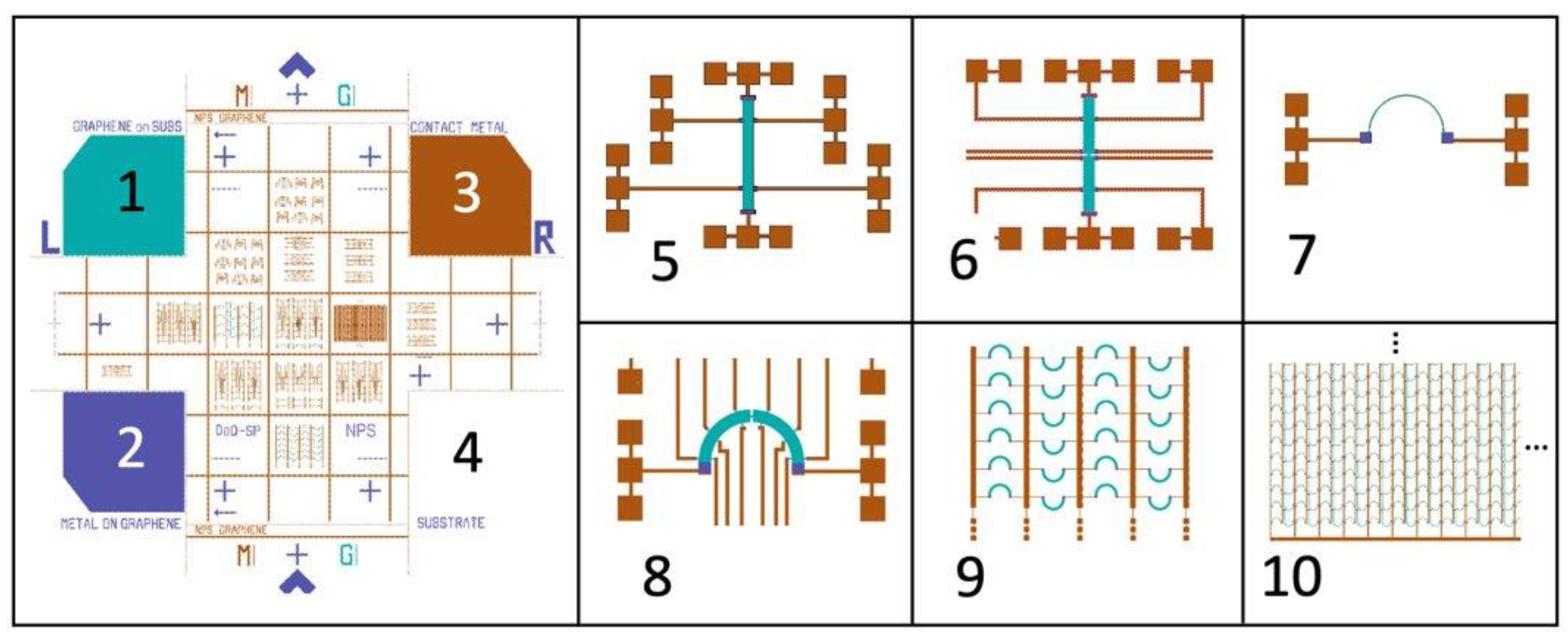
To demonstrate the process compatibility of the CVD graphene wafers, an assortment of rectangular and semicircular geometries with sizes ranging from 5 μm × 50 μm to 100 μm × 1000 μm were designed as shown in Figure 1. Successful processing of the smallest devices would demonstrate the pattern transfer resolution from the mask to the substrate [26]. Successful processing of the largest devices would test the limits of electrical continuity at millimeter scale. Semicircular device geometries were also chosen to demonstrate patterning fidelity as curved geometries may process differently than rectangular geometries, especially during development and liftoff. Lastly, device arrays were designed to test process repeatability and device yield over a 1 cm2 area. The most extensive testing was performed on the large 100 μm × 1000 μm devices on both SiO2/Si and hBN/SiO2/Si substrates in which electric field response and Hall effect measurements were performed. In addition, Raman scattering and visual inspection under a microscope were performed. With these measurements, the suitability of graphene for larger scale electrical devices and interfaces can be determined.

2.1. Fabrication

Device fabrication begins with the commercially obtained CVD graphene wafers in the form of 1 graphene/SiO2 (90 nm)/Si 4” p-doped and 1 graphene/hBN/SiO2 (285 nm)/Si 4” p-doped. Before processing, the wafers were inspected using optical microscopy for graphene coverage, irregularities, and defects. A pair of 5” masks containing the device patterns, including Hall Bars of assorted sizes and semicircular device geometries, was used for both wafers.
The first mask was used to pattern the graphene into the desired device geometries. A layer of SPR-955-0.9 photoresist was spin-coated onto each wafer followed by the pre-exposure bake. The respective wafers were then exposed to the mask pattern and then a post-exposure bake. The wafers were next developed in a CD-26 developer solution and then subjected to an O2 plasma reactive ion etch (RIE) to remove the unmasked graphene. After the RIE, the wafers were rinsed with acetone/isopropanol to remove the remaining photoresist, leaving just the patterned graphene layer.
The second mask was used to pattern the metallic contacts that interface with the graphene devices via liftoff technique. As in the first mask, a layer of SPR-955-0.9 was spin coated onto each wafer followed by a pre-exposure bake. The wafers were then exposed to the mask pattern followed by a post-exposure bake. The wafers were then developed in a CD-26 developer solution and placed in an Angstrom COVAP metal evaporator where a 5 nm adhesion layer of Cr followed by a 50 nm layer of Au were deposited. The wafers were then placed in an acetone bath and subjected to sonication for the liftoff process. At the conclusion of the liftoff process, the wafers were rinsed in deionized water and dried with compressed air. The wafers were then visually inspected and diced along 1 cm square grid lines. Diced areas that passed visual inspection—continuous graphene geometry, continuous metal contact—were then wire-bonded to a 28 terminal ceramic dual inline package (CDIP28). An overview of the wafer processing is shown in Figure 2.

2.2. Characterization

2.2.1. Raman Spectrum

Prior to patterning, Raman spectroscopy (Figure 3) was performed in order to establish a quality baseline before and after the fabrication processes. This procedure verified the survival of the graphene to the O2 plasma and acetone cleaning as well as photoresist contamination. A Renishaw inVia Raman microscope with a 514 nm wavelength laser was used at 50% power. Spectrum data was acquired in 10 s sweeps for 300 accumulations. The measurements show strong presence of the identifying G and 2D peaks and minimal presence of the disorder peaks D, D’, and D+G. For quality graphene, the 2D/G and D/G ratios should be greater than 2 and near zero, respectively [27]. For the processed samples, the 2D/G and D/G ratios were calculated to be 4.709 and 0.103 for graphene on SiO2 before etching and 4.336 and 0.159 after etching. These measurements indicate that while there is a change in quality after etching, it is not significant enough to expect adverse electrical performance.

2.2.2. Patterning Fidelity

A wide variety of geometries were patterned to determine the fidelity and robustness of the graphene patterning process at scale (Figure 4). The mask design was organized in a grid with 1 cm × 1 cm divisions allowing for redundant cells and redundant devices in the case of process defects, cleaving errors, or mishandling. The device sizes ranged from 5 μm to 100 μm in width and 50 μm to 1000 μm in length in both rectangular and semicircular geometries. Abrupt geometry changes in the form of constrictions in both rectangular and semicircular geometries were explored.
A visual inspection of the wafers indicates that the mask patterns are transferred to the graphene with high fidelity for feature sizes as small as 5 μm. This is evident as the semicircular features maintain their curvature along the inner and outer edges as well as the sharp corners present in the constricted geometries. The device patterns remain continuous for the largest features up to 1000 μm and the device arrays demonstrate the repeatability device fidelity over large areas approaching 1 cm2. High magnification also reveals artifacts of the CVD graphene process [8,10] such as grain boundaries shown as dark lines across the device, and bilayer formations shown as dark spots.

3. Results

Having demonstrated that the graphene can be patterned with conventional photolithography over a large area with features ranging from 5 μm to 1000 μm device, electrical properties were then measured. For the remainder of this report, the 100 μm × 1000 μm Hall bars on both substrates will be examined.

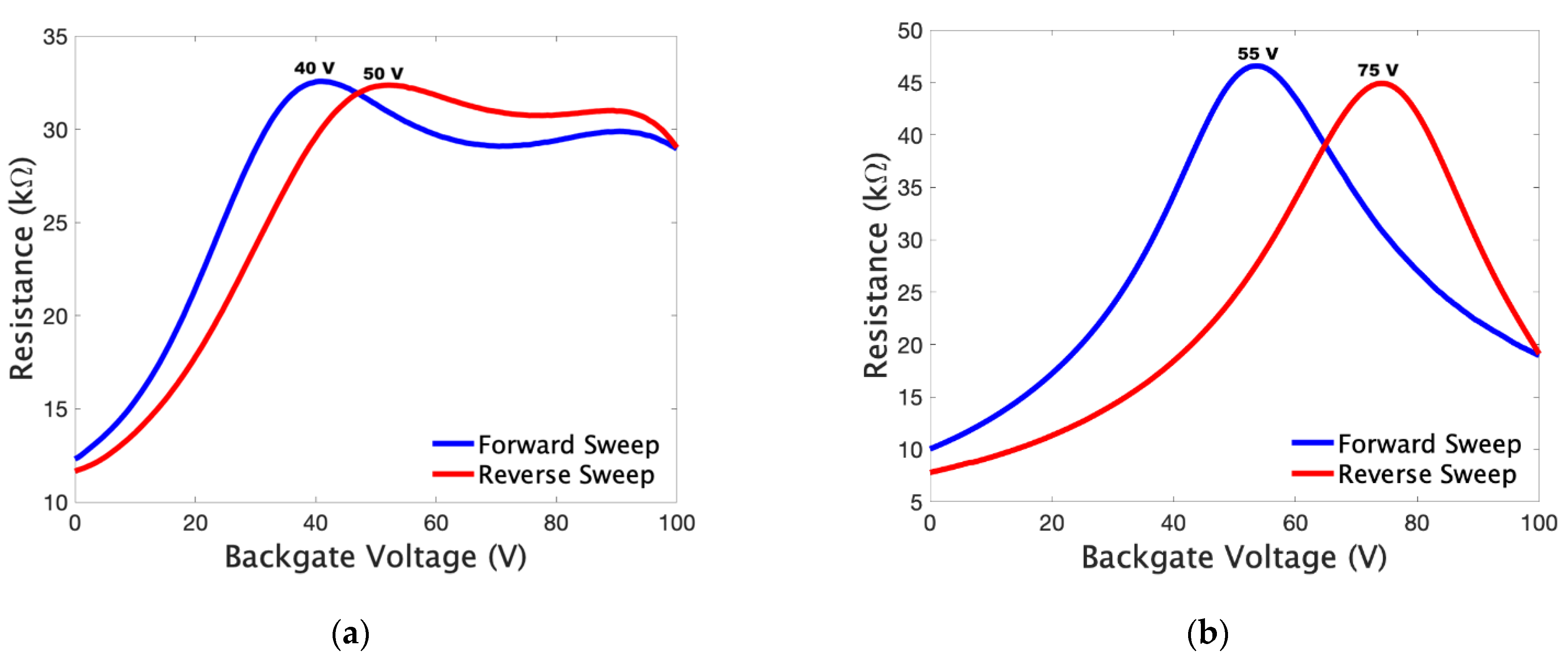
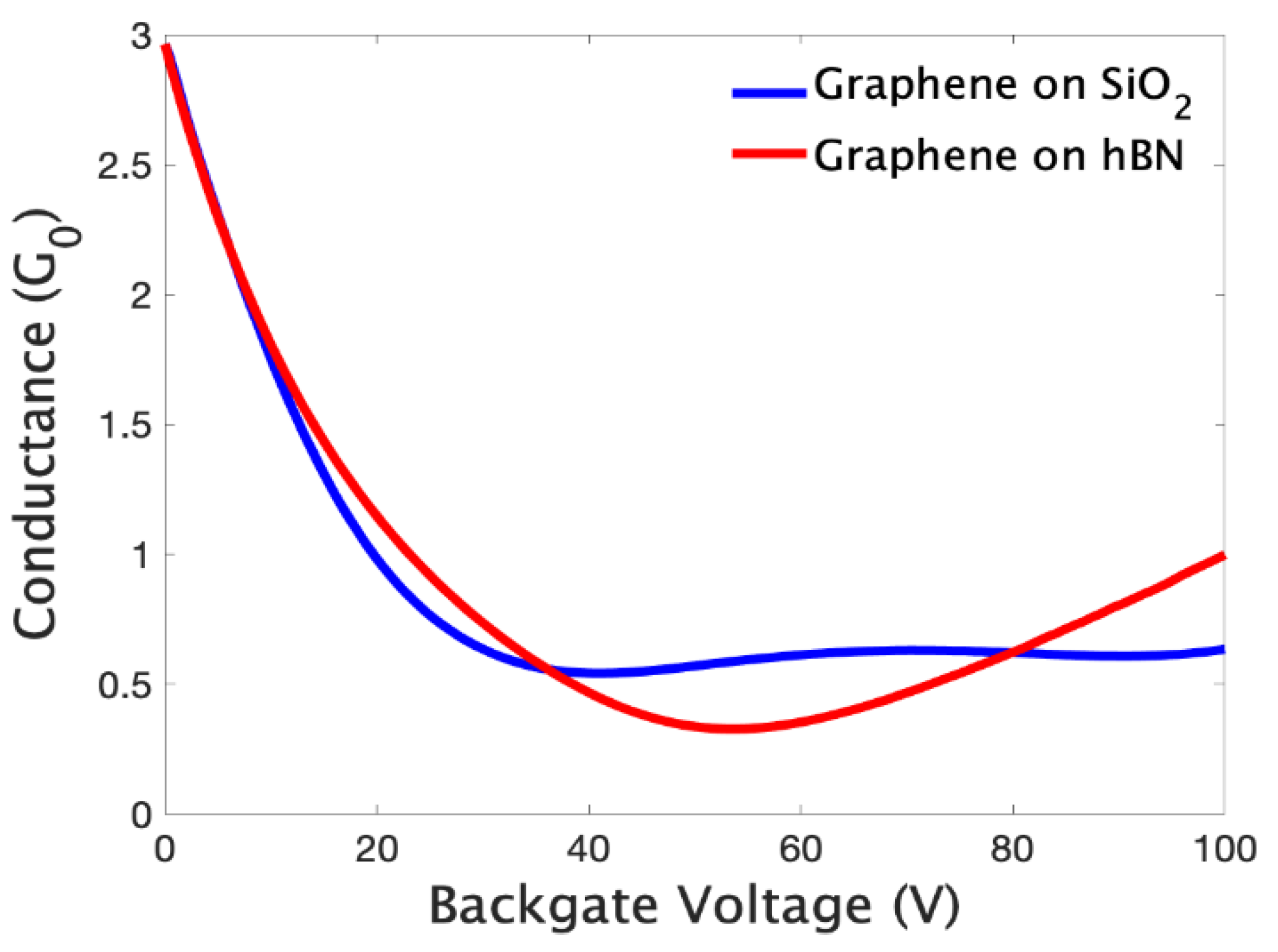
3.1. Electrical Resistance Measurements

Initial electrical characterization by 2-point and 4-point probe was performed on a Keysight B1500A semiconductor device analyzer at room temperature with no applied backgate voltage. Sheet resistance of the 100 μm × 1000 μm Hall Bar on both SiO2 and hBN were within (450 ± 5) Ω/sq. This is within the manufacturer’s specification of 430 ± 50 Ω/sq [10]. Contact resistance for the longitudinal pair was 7.7 kΩ for graphene on SiO2 and 5.5 kΩ for graphene on hBN/SiO2. The resistance measurements indicate that Ohmic contact was achieved at the graphene/metal interface.
Next, the location of the charge neutrality point (CNP) [28] for each device was determined by applying a constant DC bias of 1 V along the length of the Hall Bar and applying a backgate voltage sweep from 0 V to 100 V and back. The backgate sweeps (Figure 5) indicate that there is hysteresis [29] and the CNP location is direction dependent. For the graphene on SiO2 device, the CNP is located at 40 V in the forward direction and 50 V is the backward direction. For the graphene on hBN/SiO2 device the CNP is located at 55 V in the forward direction and 75 V in the backward direction.
From the backgate sweeps, the carrier density and charge density can be estimated with field effect methods [30], specifically with what is called a transfer length method (TLM). Based on this method the mobility, μTLM can be determined with the following expression:
μ T L M = 1 e n T L M ρ ,
where e is the electron charge, ρ is the device’s sheet resistance, and nTLM is the carrier density based on the following expression:
n T L M = C g | V g V C N P | .
This expression for carrier density is valid for the case where the gate voltage (Vg) is far away from the CNP. Lastly, the gate capacitance (Cg) is given by:
C g = ϵ ϵ 0 / t o x i d e ,
where ε0 is the permittivity of free space, ε is the relative permittivity, and toxide is the thickness of the SiO2 layer. For graphene on SiO2, the transfer length method yields a carrier density nTLM of 2.79 × 1012 cm−2 and a carrier mobility μTLM of 5.20 × 103 cm2/Vs. For graphene on hBN, transfer length method yields a carrier density nTLM of 3.84 × 1012 cm−2 and a carrier mobility μTLM of 3.78 × 103 cm2/Vs. While the mobility and density are feasibly determined with the back gate sweep data and field effect methods, these results are more useful as upper estimates. For more accurate determination of mobility and density, Hall effect measurements are required.

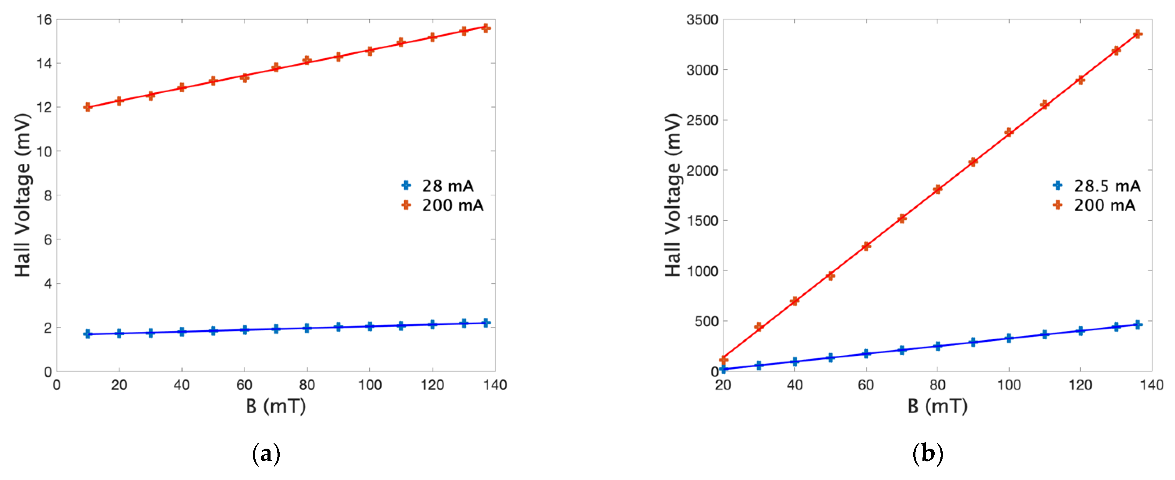
3.2. Hall Effect Measurements

Hall effect measurements were then performed on both devices with a Leybold Hall Effect apparatus at room temperature with no backgate applied. The devices were subject to a magnetic field from 20 mT to 136 mT (Figure 6). Measurements for the graphene on SiO2 were performed at two currents: 0.028 A and 0.2 A. Similarly, the graphene on hBN/SiO2 measurements were performed at 0.0285 A and 0.2 A. The Hall effect coefficients were calculated to be 1.435 × 10⁻¹¹ m3/C for graphene on SiO2 and 1.365 × 10⁻⁸ m3/C for graphene on hBN/SiO2.
Using the measured Hall coefficients, the carrier density of the devices was calculated with the relation:
n H a l l = 1 e R H ,
where RH is the Hall coefficient [31]. For graphene on SiO2, the carrier density is 4.35 × 1029 m−3 (7.8 × 1015 cm−2), while graphene on hBN/SiO2 has a carrier density of 4.6 × 1026 m−3 (8.2 × 1012 cm−2). The carrier mobility can then be determined with the relation:
μ H a l l = 1 e n H a l l ρ ,
where ρ is the resistivity. The carrier mobilities are 3.5 cm2/Vs and 3 × 103 cm2/Vs for graphene on SiO2 and graphene on hBN/SiO2. Accounting for the minimum conductivity of graphene, a modified mobility expression [3] is as follows:
μ = σ σ 0 e n H a l l ,
where σ is the device conductivity and σ0 is the device minimum conductivity. With the corrections, the mobilities are now 2.6 cm2/Vs and 2.68 × 103 cm2/Vs graphene on SiO2 and graphene on hBN/SiO2, respectively. A summary of the mobility and density for both substrates and methods is provided in Table 1.
In addition to mobility and carrier density, another metric for graphene devices is the minimum device conductivity (Figure 7). Having determined the charge neutrality point and the maximum device resistance, the minimum device conductivity in terms of the conductance quantum is calculated using [32]:
G 0 = 2 e 2 h ,
where h is Planck’s constant. Graphene on SiO2 has a minimum conductivity of 1 2 G 0 , while graphene on hBN/SiO2 has a minimum conductivity of 1 4 G 0 .

4. Discussion

While the fabricated devices are designed to be identical, the electrical and Hall Effect characterizations indicate that the graphene is highly affected by the insulating material it resides on. Starting with the resistance and CNP sweeps, graphene on SiO2 has a very broad shape, perhaps even bimodal, while graphene on hBN is well shaped and nearly Gaussian. For both wafer types, a positive CNP gate voltage is indicative of hole-dominant transport. This is expected since the Si substrate is p-doped. The broadening of the resistance curve on SiO2 is due to the presence of p-type impurities [28], since the majority carrier is expected to switch from holes to electrons past the CNP.
While the field effect method (TLM) yielded mobilities and densities that were all within the same order of magnitude for both dielectric materials, Hall effect measurements show that graphene on hBN/SiO2 is 3 orders of magnitude more responsive to an applied magnetic field. This 3 orders of magnitude difference persists in the carrier density difference and the carrier mobility difference. Graphene on SiO2 behaves like a lightly doped semiconductor in terms of its carrier density (7.8 × 1015 cm−2), but more like a metal in terms of its mobility. The low mobility of graphene on SiO2 is mostly attributed to phonon scattering [11]. The results from transfer length method were unable to capture the effects of the unintended dopants in the device which were clear in the backgate sweep and in the Hall effect measurement. This reaffirms the literature [30], where such a method is best used as an upper estimate and best applicable for intrinsic graphene.
Graphene on hBN/SiO2 agrees with other works in terms [31] of the Hall response, carrier density (8.2 × 1012 cm−2), and mobility. Both TLM and Hall effect results for mobility and carrier density agree to the same order of magnitude, with TLM providing a lower carrier density and subsequently a higher mobility. At this length scale, the graphene on hBN/SiO2 mobility of 2.68 × 103 cm2/Vs is comparable to that of GaAs [33]—a common high mobility semiconducting material. Positive Hall coefficients indicate that both devices are hole-dominant transport. This is expected as both graphene devices reside on p-doped Si, reaffirming the findings with the backgate sweeps.
Interestingly, graphene on SiO2 did have a higher minimum conductance (1/2 G0) than graphene on hBN/SiO2 (1/4 G0). This is due to the presence of impurities providing charge carriers despite the applied back gate depleting the device of intrinsic carriers from the graphene. In both cases the minimum conductance is a fraction of G0, suggesting that ballistic transport does not occur in either of these devices [11,34]. This result is also expected since the device length of 1000 μm exceeds the manufacturer’s specification of 10 μm grain size. Charge carriers in these devices will inevitably encounter scattering as they traverse the grain boundaries.
This work demonstrates the possibility of creating large-scale repeatable device patterns with conventional photolithography on commercially obtained CVD graphene wafers residing on either SiO2 or hBN/SiO2. From optical microscopy, it was shown that the pattern fidelity is high enough for semicircular shapes to maintain their curvature and abrupt geometry changes are produced without noticeable deviation and that device elements as small as 5 μm and as large as 1 mm can be accommodated. Electrical and Hall effect tests on identical 1 mm devices on both substrates showed continuity and conductivity. Even at this length, graphene on hBN/SiO2 had mobilities on the order of 103 cm2/Vs which is comparable to GaAs. Based on these results, CVD graphene on hBN/SiO2 is most suitable where high carrier mobility is crucial while CVD graphene on SiO2 is most suitable where an atomically thin electronic device is desired, but cost is also a deciding factor. The compatibility of CVD graphene with the repeatable and scalable nature of photolithography shows promise as a foundation for micron scale graphene electronic devices and a cost effective alternative to electron beam lithography.

Author Contributions

Conceptualization, J.P.; methodology, J.P. and F.A.; formal analysis, J.P.; investigation, J.P. and F.A.; writing—original draft preparation, J.P.; writing—review and editing, F.A.; visualization, F.A.; supervision, F.A; Funding Acquisition, J.P. and F.A. All authors have read and agreed to the published version of the manuscript.

Funding

This work was supported by the SMART Scholarship Program funded by the USD/R&E NDEP/BA-1 and NAWCWD NISE-219 FY21.

Data Availability Statement

Data available upon request.

Acknowledgments

The authors would like to acknowledge Dragoslav Grbovic for assisting in the fabrication process and Peter Crooker for proofreading.

Conflicts of Interest

The authors declare no conflict of interest. The funders had no role in the design of the study; in the collection, analyses, or interpretation of data; in the writing of the manuscript, or in the decision to publish the results.

References

  1. Novoselov, K.S. Electric Field Effect in Atomically Thin Carbon Films. Science 2004, 306, 666–669. [Google Scholar] [CrossRef] [Green Version]
  2. Novoselov, K.S.; Jiang, D.; Schedin, F.; Booth, T.J.; Khotkevich, V.V.; Morozov, S.V.; Geim, A.K. Two-Dimensional Atomic Crystals. Proc. Natl. Acad. Sci. USA 2005, 102, 10451–10453. [Google Scholar] [CrossRef] [Green Version]
  3. Banszerus, L.; Sohier, T.; Epping, A.; Winkler, F.; Libisch, F.; Haupt, F.; Watanabe, K.; Taniguchi, T.; Müller-Caspary, K.; Marzari, N.; et al. Extraordinary High Room-Temperature Carrier Mobility in Graphene-WSe2 Heterostructures. arXiv 2019, arXiv:1909.09523. [Google Scholar]
  4. Shishir, R.S.; Ferry, D.K. Velocity Saturation in Intrinsic Graphene. J. Phys. Condens. Matter 2009, 21, 344201. [Google Scholar] [CrossRef] [PubMed]
  5. Reina, A.; Jia, X.; Ho, J.; Nezich, D.; Son, H.; Bulovic, V.; Dresselhaus, M.S.; Kong, J. Large Area, Few-Layer Graphene Films on Arbitrary Substrates by Chemical Vapor Deposition. Nano Lett. 2009, 9, 30–35. [Google Scholar] [CrossRef] [PubMed]
  6. Chae, S.J.; Güneş, F.; Kim, K.K.; Kim, E.S.; Han, G.H.; Kim, S.M.; Shin, H.-J.; Yoon, S.-M.; Choi, J.-Y.; Park, M.H.; et al. Synthesis of Large-Area Graphene Layers on Poly-Nickel Substrate by Chemical Vapor Deposition: Wrinkle Formation. Adv. Mater. 2009, 21, 2328–2333. [Google Scholar] [CrossRef]
  7. Bae, S.; Kim, H.; Lee, Y.; Xu, X.; Park, J.-S.; Zheng, Y.; Balakrishnan, J.; Lei, T.; Kim, H.R.; Song, Y.I.; et al. Roll-to-Roll Production of 30-Inch Graphene Films for Transparent Electrodes. Nat. Nanotechnol. 2010, 5, 574–578. [Google Scholar] [CrossRef] [Green Version]
  8. Kitaura, R.; Miyata, Y.; Xiang, R.; Hone, J.; Kong, J.; Ruoff, R.S.; Maruyama, S. Chemical Vapor Deposition Growth of Graphene and Related Materials. J. Phys. Soc. Jpn. 2015, 84, 121013. [Google Scholar] [CrossRef]
  9. De Fazio, D.; Purdie, D.G.; Ott, A.K.; Braeuninger-Weimer, P.; Khodkov, T.; Goossens, S.; Taniguchi, T.; Watanabe, K.; Livreri, P.; Koppens, F.H.L.; et al. High-Mobility, Wet-Transferred Graphene Grown by Chemical Vapor Deposition. ACS Nano 2019, 13, 8926–8935. [Google Scholar] [CrossRef] [Green Version]
  10. Cheap Tubes Inc. CVD Graphene on Si-SiO2 4 Inch; Cheap Tubes Inc.: Grafton, VT, USA.
  11. Chen, J.-H.; Jang, C.; Xiao, S.; Ishigami, M.; Fuhrer, M.S. Intrinsic and Extrinsic Performance Limits of Graphene Devices on SiO2. Nat. Nanotechnol. 2008, 3, 206–209. [Google Scholar] [CrossRef]
  12. Majety, S.; Cao, X.K.; Dahal, R.; Pantha, B.N.; Li, J.; Lin, J.Y.; Jiang, H.X. Semiconducting Hexagonal Boron Nitride for Deep Ultraviolet Photonics. In Quantum Sensing Nanophotonic Devices IX; International Society for Optics and Photonics: Bellingham, WA, USA, 2012. [Google Scholar] [CrossRef]
  13. Garcia, A.G.F.; Neumann, M.; Amet, F.; Williams, J.R.; Watanabe, K.; Taniguchi, T.; Goldhaber-Gordon, D. Effective Cleaning of Hexagonal Boron Nitride for Graphene Devices. Nano Lett. 2012, 12, 4449–4454. [Google Scholar] [CrossRef] [PubMed]
  14. Kim, K.K.; Kim, S.M.; Lee, Y.H. A New Horizon for Hexagonal Boron Nitride Film. J. Korean Phys. Soc. 2014, 64, 1605–1616. [Google Scholar] [CrossRef]
  15. Yamoah, M.A.; Yang, W.; Pop, E.; Goldhaber-Gordon, D. High-Velocity Saturation in Graphene Encapsulated by Hexagonal Boron Nitride. ACS Nano 2017, 11, 9914–9919. [Google Scholar] [CrossRef] [PubMed]
  16. Kim, S.M.; Hsu, A.; Araujo, P.T.; Lee, Y.-H.; Palacios, T.; Dresselhaus, M.; Idrobo, J.-C.; Kim, K.K.; Kong, J. Synthesis of Patched or Stacked Graphene and HBN Flakes: A Route to Hybrid Structure Discovery. Nano Lett. 2013, 13, 933–941. [Google Scholar] [CrossRef] [PubMed]
  17. Stehle, Y.; Meyer, H.M.; Unocic, R.R.; Kidder, M.; Polizos, G.; Datskos, P.G.; Jackson, R.; Smirnov, S.N.; Vlassiouk, I.V. Synthesis of Hexagonal Boron Nitride Monolayer: Control of Nucleation and Crystal Morphology. Chem. Mater. 2015, 27, 8041–8047. [Google Scholar] [CrossRef]
  18. Guo, Q.; Li, C.; Deng, B.; Yuan, S.; Guinea, F.; Xia, F. Infrared Nanophotonics Based on Graphene Plasmonics. ACS Photonics 2017, 4, 2989–2999. [Google Scholar] [CrossRef]
  19. Huang, S.; Song, C.; Zhang, G.; Yan, H. Graphene Plasmonics: Physics and Potential Applications. Nanophotonics 2016, 6, 1191–1204. [Google Scholar] [CrossRef]
  20. Kim, J.Y.; Cho, N.S.; Cho, S.; Kim, K.; Cheon, S.; Kim, K.; Kang, S.-Y.; Cho, S.M.; Lee, J.-I.; Oh, J.-Y.; et al. Graphene Electrode Enabling Electrochromic Approaches for Daylight-Dimming Applications. Sci. Rep. 2018, 8, 16924. [Google Scholar] [CrossRef]
  21. Woo, Y. Transparent Conductive Electrodes Based on Graphene-Related Materials. Micromachines 2018, 10, 13. [Google Scholar] [CrossRef] [Green Version]
  22. Beiranvand, B.; Sobolev, A.S. A Proposal for a Multi-Functional Tunable Dual-Band Plasmonic Absorber Consisting of a Periodic Array of Elliptical Grooves. J. Opt. 2020, 22, 105005. [Google Scholar] [CrossRef]
  23. Beiranvand, B.; Sobolev, A.S.; Sheikhaleh, A. A Proposal for a Dual-Band Tunable Plasmonic Absorber Using Concentric-Rings Resonators and Mono-Layer Graphene. Optik 2020, 223, 165587. [Google Scholar] [CrossRef]
  24. Dong, Y.; Xiong, L.; Phinney, I.Y.; Sun, Z.; Jing, R.; McLeod, A.S.; Zhang, S.; Liu, S.; Ruta, F.L.; Gao, H.; et al. Fizeau Drag in Graphene Plasmonics. Nature 2021, 594, 513–516. [Google Scholar] [CrossRef] [PubMed]
  25. Morgado, T.A.; Silveirinha, M.G. Active Graphene Plasmonics with a Drift-Current Bias. ACS Photonics 2021, 8, 1129–1136. [Google Scholar] [CrossRef]
  26. Liu, C. Foundations of MEMS, 2nd ed.; Prentice Hall: Upper Saddle River, NJ, USA, 2012; ISBN 978-0-13-249736-7. [Google Scholar]
  27. Childres, I.; Jauregui, L.A.; Park, W.; Cao, H.; Chen, Y.P. Raman Spectroscopy of Graphene and Related Materials. New Dev. Photon Mater. Res. 2013, 1, 1–20. [Google Scholar]
  28. Wojtaszek, M. Graphene: A Two Type Charge Carrier System. Master’s Thesis, Faculteit der Wiskunde en Natuurwetenschappen, Groningen, The Netherlands, 2009. [Google Scholar]
  29. Guo, Y.; Wei, X.; Shu, J.; Liu, B.; Yin, J.; Guan, C.; Han, Y.; Gao, S.; Chen, Q. Charge Trapping at the MoS-SiO2 Interface and Its Effects on the Characteristics of MoS Metal-Oxide-Semiconductor Field Effect Transistors. Appl. Phys. Lett. 2015, 106, 103109. [Google Scholar] [CrossRef]
  30. Zhong, H.; Zhang, Z.; Xu, H.; Qiu, C.; Peng, L.-M. Comparison of Mobility Extraction Methods Based on Field-Effect Measurements for Graphene. AIP Adv. 2015, 5, 057136. [Google Scholar] [CrossRef]
  31. Hui, Y.X.; An, N.; Chen, K.; Li, X.J.; Li, W.L.; Ren, Z.Y. Research on Hall Effect of Graphene by Var Der Pauw Method. Adv. Mater. Res. 2015, 1120–1121, 383–387. [Google Scholar] [CrossRef]
  32. Van Wees, B.J.; van Houten, H.; Beenakker, C.W.J.; Williamson, J.G.; Kouwenhoven, L.P.; van der Marel, D.; Foxon, C.T. Quantized Conductance of Point Contacts in a Two-Dimensional Electron Gas. Phys. Rev. Lett. 1988, 60, 848–850. [Google Scholar] [CrossRef] [Green Version]
  33. Sze, S.; Irvin, J. Resistivity, Mobility and Impurity Levels in GaAs, Ge, and Si at 300 K. Solid-State Electron. 1968, 11, 599–602. [Google Scholar] [CrossRef]
  34. Tse, W.-K.; Hwang, E.H.; Sarma, S.D. Ballistic Hot Electron Transport in Graphene. Appl. Phys. Lett. 2008, 93, 023128. [Google Scholar] [CrossRef] [Green Version]
Figure 1. Mask layout and some of the fabricated structures. (14) Control areas of: graphene, contact metal on graphene, contact metal, and SiO2 substrate, respectively. (5) A 100 μm × 1000 μm Hall Bar. (6) A 100 μm × 1000 μm Hall Bar with a 20 μm constriction. (7) A 10 μm × 1000 μm arc. (8) A 100 μm × 1000 μm arc with a 20 μm constriction. (9) A 4 × 4 array of 100 μm × 1000 μm arcs. (10) Section of a 44 × 85 array of 5 μm × 100 μm arcs.
Electronics 11 00752 g001
Figure 2. Overview of the fabrication process. (1) 4” wafer with graphene on SiO2/Si or hBN/SiO2/Si. (2) Graphene patterning: deposition and exposure of photoresist layer with 1st mask. (3) Photoresist layer after developing of 1st mask pattern. (4) Removal of graphene in non-patterned areas with O2 plasma etch. (5) Acetone removal of 1st photoresist layer. (6) Metal patterning: deposition and exposure of photoresist layer with 2nd mask. (7) Photoresist layer after developing 2nd mask pattern. (8) Deposition of 5 nm Cr layer. (9) Deposition of 50 nm Au layer. (10) Liftoff of 2nd mask photoresist and excess metal.
Electronics 11 00752 g002
Figure 3. Raman spectra of graphene on SiO2 before O2 plasma etch and after. The identifying peaks G (1580 cm−1) and 2D (2690 cm−1) are present. The disorder peaks D (1350 cm−1), D’ (1620 cm−1), and D+G (2940 cm−1) are minimal.
Electronics 11 00752 g003
Figure 4. Fabricated devices (1) A 100 μm × 1000 μm Hall Bar with a 5 μm constriction at 5× magnification. (2) 40× magnification of the 5 μm constriction from (1). (3) A 100 μm × 1000 μm Hall Bar at 5× magnification. (4) A 100 μm × 1000 μm arc with a 20 μm constriction at 5× magnification. (5) 40× magnification of the 20 μm constriction from (4). (6,7) 100 μm × 1000 μm arc elements of a 4 × 4 array at 5× magnification. Images were taken with low illumination to increase the contrast and visibility of the graphene areas.
Electronics 11 00752 g004
Figure 5. Backgate sweeps to locate the charge neutrality point for (a) graphene on SiO2 and (b) graphene on hBN/SiO2.
Electronics 11 00752 g005
Figure 6. Hall Effect measurements for (a) graphene on SiO2 and (b) graphene on hBN/SiO2.
Electronics 11 00752 g006
Figure 7. Device conductance in units of the quantum of conductance for graphene on SiO2 and graphene on hBN/SiO2.
Electronics 11 00752 g007
Table 1. Summary of carrier density and mobility from TLM and Hall effect methods on both dielectric materials.
Dielectric MaterialnTLM
(cm−2)
nHall
(cm−2)
RHall
(m3/C)
μTLM
(cm2/Vs)
μHall
(cm2/Vs)
μ
(cm2/Vs)
Graphene on SiO22.79 × 10127.8 × 10151.435 × 10−115.20 × 1033.52.6
Graphene on hBN3.84 × 10128.2 × 10121.365 × 10−83.78 × 1033 × 1032.68 × 103
Publisher’s Note: MDPI stays neutral with regard to jurisdictional claims in published maps and institutional affiliations.

