1. Introduction
Laser trimming of film and foil resistive elements (RE) is currently the most popular means for obtaining the required resistance value both for a single chip-resistor or microwave attenuator and for an integrated one into a hybrid integral circuit [
1,
2,
3]. This is due to the fact that even modern technologies for the production of passive components do not allow manufacturing of a precision element with the required accuracy characteristics without additional adjustment. Unlike chemical or electro-discharge treatment, laser trimming is a universal means concerning both film materials and installed surface-mounted elements and has the best outlook as far as automation is concerned.
Currently, a significant amount of research is being carried out in the field of this technology, for example, in terms of technological aspects, the influence of trimming on the stability of the characterization of trimmed thick-film and LTCC resistors [
4], as well as resistors from a novel CuAlMo thin film resistor material [
5] and CrSi thin film resistor [
6]. Significant research is being done into the effect of varying laser trim patterns on several performance parameters of thin film resistors (such as the temperature coefficient of resistance (TCR) and the target resistance value) [
7], as well as the long-term stability of characteristics [
8]. In addition, a number of researchers are studying the effect of the configuration of the resistors themselves on their characteristics when trimming [
9,
10]. Special attention is paid to foil resistors [
11].
Since the requirements, both in terms of technical parameters of the process and final products, and in terms of economic efficiency indicators, are constantly increasing, new equipment for laser trimming with higher performance and an improved set of functions appears regularly [
12,
13,
14,
15,
16]. Modern research allows developing and implementing new functions. One of the problems, which, in our opinion, significantly increases the level of automation and economic efficiency of the trimming process, as well as the quality of manufactured products, is the development, creation, and implementation in modern equipment of a mechanism for trimming process simulation for fast and accurate prediction of the resistor value, while effecting a configuration for a trimming cut.
There are many approaches to the description of the direct conductive medium of RE and in application to the modeling of laser trimming. For example, in [
17,
18], the authors used the finite element method to determine the potential field in a resistive film, which is described by the Laplace equation in partial derivatives. The calculation method is based on a special application of Green’s boundary formula [
19].
In the following papers, the authors also use modeling of the correction of the geometry of a conductive resistive medium without describing the method of building models. Thus, in [
10], the authors give an overview of the influence of the configuration of the resistive film and the configuration of trim cuts on the characteristics of resistors.
In the article [
20], the authors propose an approach to the representation of a resistor based on conformal mapping methods. A brief description of the process of constructing a model of a rectangular resistive film with a U-cut is given. Additionally, the conformal mapping method is used to study the trimming of resistors with an additional third pad [
21] and arbitrary shape resistors [
22]. The disadvantage of this method is the lack of universality; in other words, for each cut shape with different parameters, a new model is required.
Some researchers argue that conformal mapping and Eigenfunction decomposition are all well-known methods for finding the solution to Laplace’s equation in two dimensions but are practical for only small problems: for larger designs, they require a lot of computing resources [
23]. It is proposed to solve the Laplace equation using the relaxation method with elements of heuristics. The idea is to break complex polygons into simpler parts to extract resistance [
24,
25]. However, according to the authors of the work, the accuracy of their models is in the region of 10%, which is unacceptable for modern resistor building with accuracy requirements of 1 … 0.01%.
Ramirez-Angulo, et al. made a significant contribution to the study of the laser trimming process and the construction of simulation systems. In their works [
26,
27,
28], based on the solution of the Laplace equation by the finite element method, the authors demonstrated the developed program FIRE (FIlm REsistors). The model underlying this program works for non-homogeneous and homogeneous films. As a result of which it was possible to take into account separately the effect of changing the parameters of the resistive film zone adjacent to the cut (heat affected zone (HAZ)). This made it possible to conduct a number of important studies in the field of the influence of laser radiation parameters on the long-term stability of resistors. The most detailed topic of model building and simulation is disclosed in the works of Phillip Sandborn and Peter A. Sandborn. In [
29], they describe simple models based on dividing a RE into rectangles, with further calculation of the total resistance based on Ohm’s law. These models, according to the authors, are approximate and more reasonable for educational purposes. Similar models are used by other researchers in [
30,
31]. The model developed in this study [
32] is a finite difference model, formulated similarly to [
26]. In this case, it is required to determine the potential field in a resistance film and is governed by the Laplace equation with partial derivatives. The authors used this model to explore their proposed random trimming approach to obtain highly accurate trimming results. However, the paper does not provide the algorithm for generating the model; it is also not clear how the model is corrected when performing a trimming cut. At the same time, the paper gives examples of the trimming characteristics of the simulated resistors obtained using this model, the current distribution field. An example of modeling the temperature load on various sections of the conductive film due to power dissipation during operation in the circuit is also given, which is especially important for the resistors built into the multilayer printed circuit board considered in this paper.
Additionally, a number of works that made a significant contribution to the study of the modeling of the trimming process were published by Klaus Schimmanz and Arnulf Kost. In their research, they compared methods for solving the Laplace equation: the finite element method, the finite difference method, and the boundary element method, indicating the speed for a number of practical problems [
33,
34].
After a deep analysis of the above studies, in our opinion, the most suitable approach here is circuit modeling of the trimming process for film RE, which allows passing to macrolevel models, i.e., models with lumped parameters.
Considering the problem of circuit modeling, in which the RE is considered as a macro-level model and described by algebraic equations for unknown nodal values of functions, we talked about the selection of elements, which are further considered as a indivisible unit-elementary resistors (ER). In this case, we formed a mathematical model by combining topological equations obtained on the basis of graph theory and Kirchhoff’s laws and component equations formed by applying Ohm’s laws to the grid model of the resistor [
35,
36,
37].
This approach allowde us to consider models of simple and composite film resistors of arbitrary configuration and disclose internal information about the electrophysical processes occurring in the RE both during trimming and during further operation of the product.
The authors previously outlined the process for creating a circuit mesh model for the process of a film resistor trimming in a situation when a direct current source is used in the circuit of the measuring device [
38]. However, this variant is partially restricted for use, inter alia, when trimming resistors within a circuit board, on which active elements have already been installed. Current supply in this situation may result in inaccurate measurements due to operation of semi-conductor elements within the circuit or burning of these elements. Therefore, constant voltage sources are often used in measuring devices.
In connection with the above, the purpose of this work, being the follow-up of the previously submitted article [
38], is to develop a circuit model for the process of film REs laser trimming using a measuring voltage source, as well as an algorithm for correcting this model during laser trimming. To achieve this goal, it is necessary to perform the following tasks: to create a basic representation of the circuit model of the conductive medium of the RE, to formulate a mathematical description of the model of the conductive resistive medium, and to develop an algorithm for calculating the parameters of the resistor when changing the circuit model in the process of laser trimming. Each task is highlighted in a separate section of the paper. We preface the conclusion with a detailed discussion section.
2. Building a Circuit Model for a Film Resistor Conductive Medium
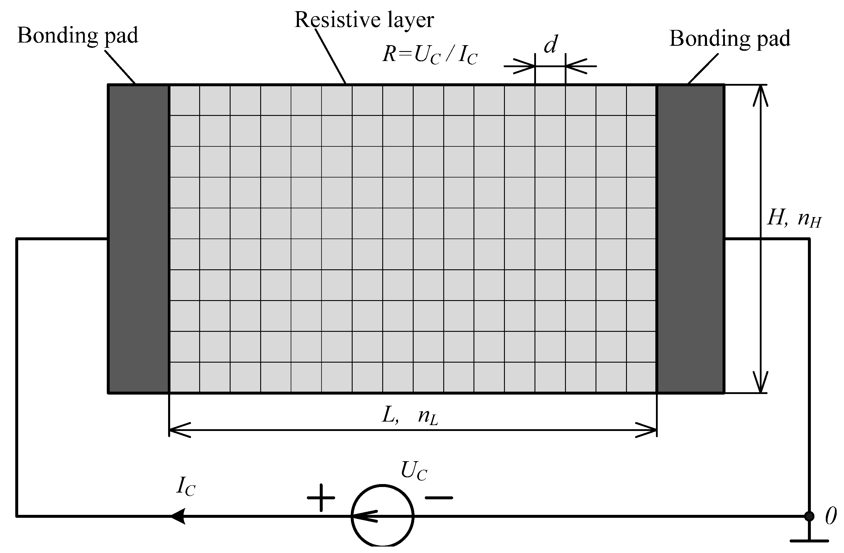
If a rectangular film resistor has the length
and the width
, then the current-conducting medium will be approximated by a discrete mesh of ERs
with
size and the number of nodes
and
, respectively (see
Figure 1).
Since the number of horizontal branches in each horizontal line is one more than the number of horizontal internal nodes, the number of horizontal branches in each horizontal line will be equal to
and the total in the model is
. The number of vertically arranged branches in each vertical line will be one less than the number of vertical nodes, since the top and bottom of the conductive resistive film model ends with a node, not a branch. Accordingly, in each vertical line there will be
branches and in total in the model
vertical branches. The total number of branches
in the model will be determined as follows:
The total number of internal model nodes will be determined as follows:
If the initial resistance
is measured before the trimming starts, the resistance value ER
included between the mesh nodes can be calculated depending on the number of discretization points of the resistive field along the width and the length
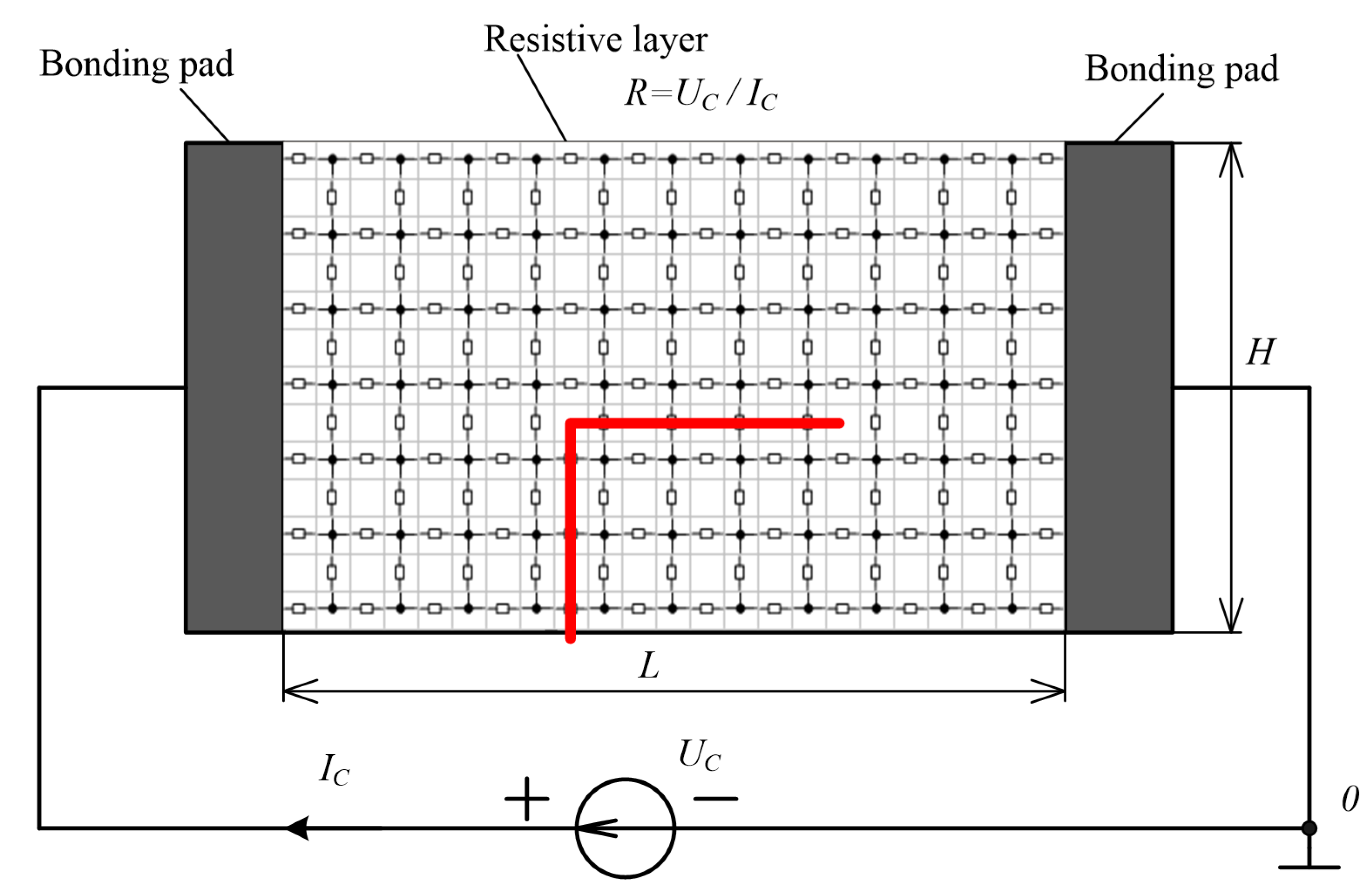
The resistor trimming process at the circuit model can be characterized by removing ER situated at the laser cut path (see
Figure 2). As the distribution of current and power in different fields of ER changes, the RE resistance value cannot be calculated according to the simplest correlation given above.
3. Mathematical Representation of the Resistive Conductive Medium Circuit Model
The source data for forming the circuit mathematical models at a macro level are component and topological equations.
Component equations are equations that represent the properties of single elements (components). In other words, these are equations for mathematical models of elements; elemental resistors connecting the mesh nodes in the case under consideration.
Topological equations represent the correlations of elements within a circuit under simulation and render Kirchhoff’s laws for voltages and currents. Following Kirchhoff’s law for voltage, the sum of voltages at components along any closed circuit in an equivalent circuit equals zero, whereas, according to Kirchhoff’s law for current, the sum of currents equals zero in any closed section of a closed circuit.
3.1. Component Equations of the Simulation Model
In electrical systems, two types of phase variables are distinguished: phase variables of the type of potential (electrical voltage) and type of current (electrical current). Each component equation characterizes the reference between different-type phase variables, referring to one component (e.g., Ohm’s law defines the reference of voltage and current in a resistor), whereas a topological equation defines the reference between one-type phase variables in different components.
In a circuit model of a conductive resistive medium, the components are two-pole elements—resistors included between the mesh nodes—whereas phase variables are electrical voltages and currents on these elements. The component equations of branches for the circuit model under consideration, where elements are represented by resistors
, included between nodes, are formed based on Ohm’s law and have been expressed as:
where
is a voltage at a
resistor and
is a current in a
resistor.
In a matrix form:
where
is the vector of voltages at resistors in a mesh for
sizing,
is the vector of currents at resistors for
sizing, and
—is a square matrix of branch resistor resistances for
sizing.
Component equations can also be defined referring to the ERs conductivity:
where
is ER’s conductivity, which is included between the mesh nodes.
In a matrix form, this correlation is expressed as
where
—is the square matrix of resistors conductivity for
sizing.
3.2. Topology of Circuit Model
A topological structure defines a way of connecting the components, i.e., the configuration. With this, the type of components is not important. A topological circuit structure is defined by a topological graph or by topological matrices [
6]. A natural and easy way for defining information on the way of connecting and on reference positive directions for currents and voltages for the branches of a circuit model is an oriented graph, which would correspond to a given circuit and is built following the rule: each element of the circuit with two terminals shall be replaced by a linear segment called a branch, with an arrow pointing at the positive direction for the current via this branch. This arrow also defines the reference direction for the branch voltage: the arrow starts at the terminal with a positive potential.
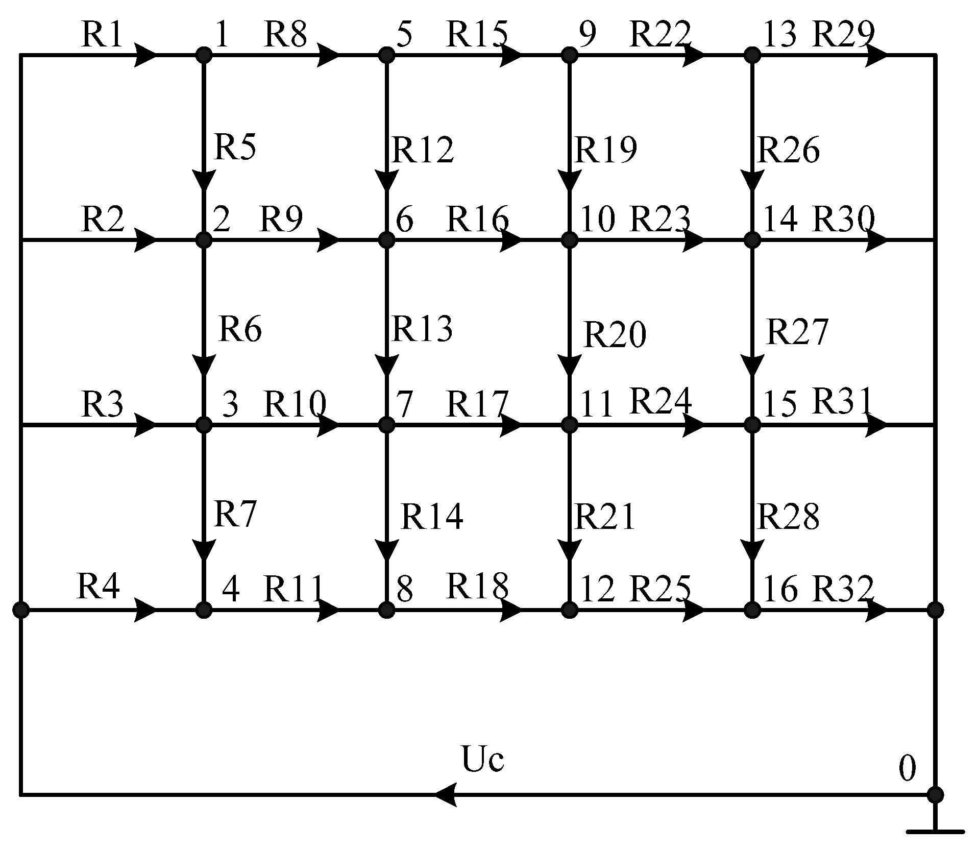
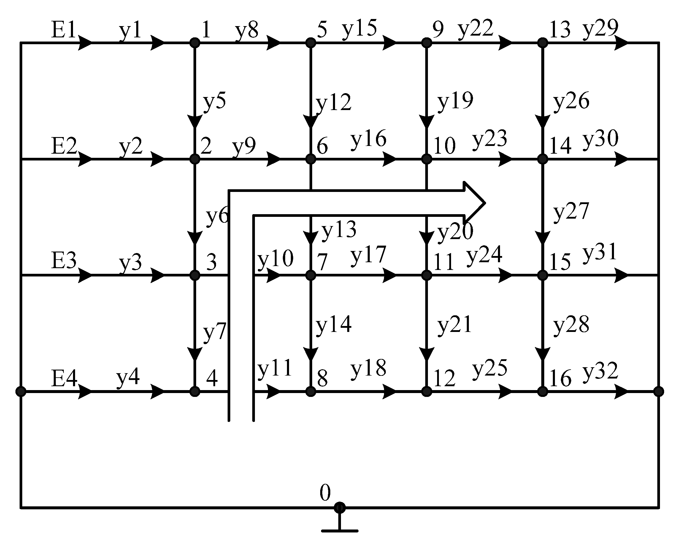
Figure 3 shows an example of an oriented graph, corresponding to a simplified RE circuit model with a 4 × 4 node sizing. The graph contains 17 nodes, including the external zero-base node and 32 branches.
The information contained in the oriented graph can fully be represented by a topological matrix called the incidence matrix. In a full ‘node branch’ type incidence matrix, the number of lines equals the number of graph nodes (points), whereas the number of columns equals the number of branches.
For an oriented graph with nodes and branches, the incidence matrix is , a matrix of sizing. With this, , where if branch is connected with node and starts from it. The arrow points from the node, , if the branch is connected with the node and enters it, and the arrow points towards i node, , if the branch is not connected with the node.
Any line can be excluded from the matrix without losing data because such a line can be restored any time following the rule that each column shall be completed to a zero-sum. A matrix obtained from a full incidence matrix by excluding one line is called a reduced incidence matrix, or just an incidence matrix (node matrix), and is denoted as .
While solving practical problems, the line corresponding to the basis zero node is usually excluded. With this, the reduced incidence matrix will be sizing. Its lines are linearly independent, ; the number of inner nodes of the circuit model.
3.3. Correlation between the Variables of the Circuit Model Branches
Let us form Kirchhoff’s law for voltage for the inner
nodes of the circuit, i.e., for all nodes except for the basis zero one:
Currents for branches of the circuit model are unknown—their number exceed the number of equations in the system (1), —hence the system has multiple solutions and cannot be solved single-valued referring to currents of branches. To get a single-valued solution, additional properties of the circuit model should be considered.
Node voltages of the circuit are connected via the incidence matrix. As the direction of the graph branch coincides with the direction of the current in an element, the node from which the current starts has a higher potential than a node where this current inflows. As a result, the voltage of each branch
is the difference between voltages
and
in neighboring nodes
and
, to which this branch is connected:
The information about connected nodes for a -branch and about its direction is contained in the -column of the incidence matrix. For example, by multiplying in the sequence the transposed columns of the incidence matrix by the column vector of the node voltages , we obtain the voltages at the model branches.
As a result, using the transposed
incidence matrix, we obtain the interpretation for the voltages vector for the model branches
via the vector of node voltages
:
This transformation is called the transformation of nodes, and with this we can interpret the high-dimensional voltages vector for branches via a vector of a smaller dimension for node voltages , decreasing the degree of order for the problem being solved. Equations (1) and (2) are the record for Kirchhoff’s laws for currents and voltages in a circuit model.
Proceeding from nodes transformation (2), we obtain the correlation of the branch currents vector with the nodes voltages vector, which has a smaller degree of order:
Expression (1) for the Kirchhoff’s law for current is then expressed as
Expression (3) is a system of linear algebraic equations relating to the node voltages vector , which has a much smaller degree of order compared to branch voltages vectors and current vectors . The matrix of the system is a square non-generate one, with sizing.
3.4. Forming the System of Equations for the Circuit Mathematic Model and Its Solution Relating to Node Voltages
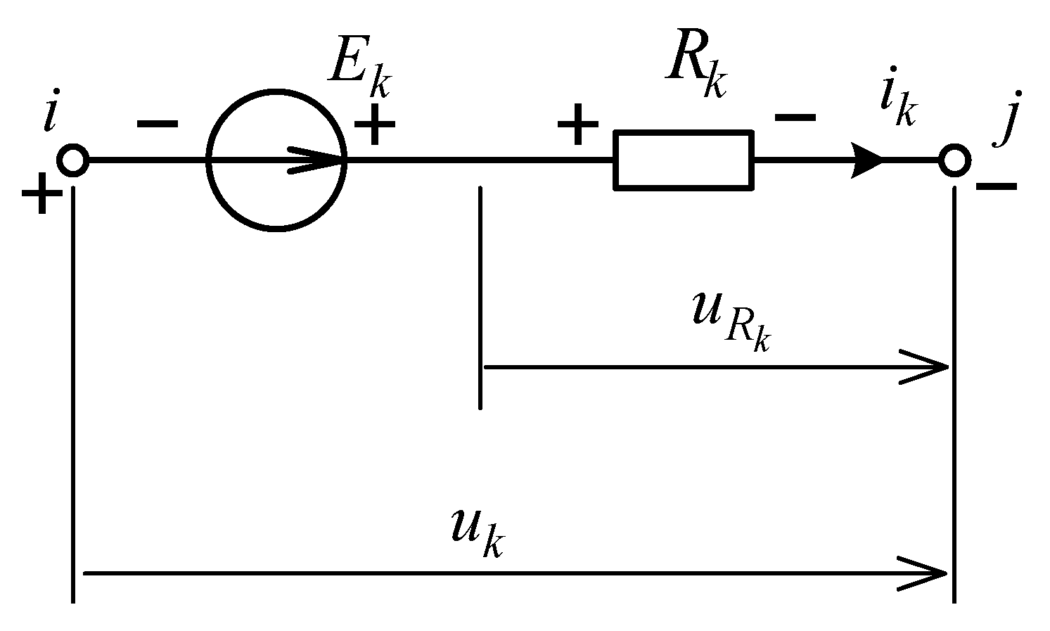
As the structure of the replacement circuit within each separate branch of the circuit model for a case with a voltage measuring source differs from the previously defined one [
38], we considered each branch of the circuit model in a general form, which consist of a series connection of the resistor
and the voltage source
, as shown in
Figure 4. With this, all the branches of the circuit model have a same-type structure, and depending on which parameter equals zero,
or
, the general branch becomes either a resistor or a voltage source.
With this, the correlation of branch currents and voltages can be determined not only by component equations and their conductivities but also by branch voltage sources:
In the matrix form, the correlation between branch currents and voltages can be defined by this proportion:
where
is the vector of external voltages of branches, which are defined as follows:
Taking into consideration transformations of nodes (2), we obtain a correlation of currents vector for general branches with the vector of node voltages, concerning the vector of the external voltages sources:
Expression (3) for the Kirchhoff’s law current can then expressed as:
From here, we obtain a system of linear algebraic equations relating to the vector of node voltages
, which is much smaller in the degree of order compared to branch vectors of voltages
and currents
:
The matrix of the system
is a square non-generate one of
sizing; it is called the matrix of nodes total conductivity [
7]
The external sources of voltages define the right part of the system
, which is a vector of the equivalent node current sources
of
sizing:
The forms system of equations is expressed as:
It has the unambiguous solution relating to the vector of node voltages (potentials), the components of which are finally defined by the value of the external measuring voltage
. Equation (6) is called a node equation, and the process of solving it, relating to the vector of node voltages
, is called node analysis:
For equal resistances
and conductivities
of the resistance mesh branches, the square matrix of mesh resistors conductivities of
sizing can be expressed as the product of a unit matrix
and scalar cofactor of conductivity
for each branch:
System (4), relating to the node potentials, is then simplified due to reducing the conductivity in the left and right parts and is expressed as:
We called the obtained system of equations the reduced system of node equations and the matrix of node conductivities
the reduced matrix of node conductivities. The elements of this matrix do not depend on the ER mesh resistances; they are integer values, reflecting the structure (the topology) of the circuit model and are defined by the number of mesh elements connected to a certain node. The solution of the reduced system (6) does not depend on the mesh ER resistances or conductivities. The vector of the external branch voltages sources
has only got
in the first non-zero elements, each equaling the external measuring voltage
,
, while the right part of the system (6) can be defined by this vector:
In a general case, solving System (7), relating to node voltages
:
voltages at branches based on node transformation are calculated (2),
voltages at mesh resistors,
and, respectively, branch currents (4),
Based on the sum of currents in the first column of the ER mesh, the external result measuring current flowing through a film resistor is calculated:
and the resulting resistance of a film resistor,
4. Evolution of Resistor Parameters as the Circuit Model Is Restructured during RE Trimming
During the process of resistor trimming and change of structure of the circuit model due to the removal of mesh resistors at the cut trajectory, only the matrix of node conductivities changes, while the vector of equivalent current sources remains unchanged. This can be explained by the absence of change during the trimming process for circuit model voltage sources, defined by the source of the measuring voltage and connected in a series with the resistors of the left column of the resistors mesh. As a result, the vector in the right part of the system remains unchanged.
Changes are made according to the previously defined node equation of the system (6) and considering the node numbers, to which the removed ER had been connected. This process is similar to actions taken for a system model with the measuring source of direct current. If a -branch is removed, which is directed from node to node with conductivity , then in a matrix , is removed in four places: is twice deducted from elements and of matrix in the diagonal line and twice is added to non-diagonal elements and . After making each correction, System (6) can be solved anew, relating to node voltages, and after that, the film resistor resistance value should be recalculated.
Let us explore the cut trajectory shown in the graph of the simplified circuit model in
Figure 5. At the first stage, ER
with conductivity
, connected to nodes 4 and 8, is removed. As a result, in matrix
of System (6), diagonal elements
and
are reduced by
(by 1 in a reduced matrix) and elements
and
are increased by
(by 1 in a reduced matrix) and become zero values. Stages 2, 3, and 4 are performed in the same way, with the removal of branches with numbers 10, 13, and 20, respectively.
5. Discussion
The main requirements for models are the requirements of adequacy, accuracy, and economy. The model only approximately reflects some properties of the object. Adequacy takes place if the model reflects the given properties of the object with acceptable accuracy. Accuracy is understood as the degree of correspondence between the estimates of the properties of the same name of the object and the model. Economy (computational efficiency) is determined by the cost of resources required to implement the model. Since mathematical models are used, the efficiency will be characterized by the cost of computer time and memory. Adequacy is assessed by the list of reflected properties and areas of adequacy. The area of adequacy is the area in the parameter space, within which the errors of the model remain within acceptable limits. Additionally, important requirements include ease of implementation and the possibility of a fully-fledged (without significant restrictions) application for the target task.
As shown in the introduction, there are different approaches to building a resistor model in the laser trimming process. They are all more or less adequate, accurate, and effective. As part of the comparative analysis, the following remarks should be made.
From the point of view of the possibility of a fully-fledged application, the model built within the framework of this work on the basis of topological and component equations, as well as models based on conformal mappings, numerical methods for solving the Laplace equation, and the method of rectangles, can be built into control systems for industrial laser installations and perform the function of preliminary calculation of the resistance value when performing a particular cut.
If we talk about implementation, it is obvious that the simplest are the models based on the method of rectangles (the simplest equations are solved) and nodal analysis (a system of linear algebraic equations), while the implementation of other methods requires the solution of differential equations in partial derivatives, together with boundary conditions. In addition, the implementation of the method of conformal mappings is hampered by the need to reform the initial conditions with each change in the configuration of the resistive film, and this happens all the time during the trimming process. A significant advantage of nodal analysis is also that, when using it, it is much easier to apply various algorithms for finding optimal trajectories, since when varying the geometry of the trimming cut according to the algorithm given in
Section 4 of this work, it is easy to change the coefficients of the system matrix, eliminating the need to rebuild the model with a start. It should also be borne in mind that the system matrix is a tridiagonal highly sparse matrix, which allows us to consider various algorithms for accelerated calculations.
For a comparative assessment of the adequacy, accuracy, and efficiency of the models, it is necessary, first of all, to implement the model obtained in the study in the form of a simulation program. However, even after such an implementation by the authors of this work, it will be very difficult to conduct a comparative analysis. The fact is that the authors of most studies, for all the undoubted significance of their work, either do not study the obtained models for accuracy (there is no comparison of the simulated value in the simulation system with the real values of the resistance of the trimmed resistors) or do not provide data on the speed of the calculation algorithms according to the proposed models. In addition, a number of researchers do not provide a description of the construction of the model, and therefore it is not possible to assess which of the methods was used. We assume that this is due to the fact that the authors did not have the goal of embedding the obtained models and algorithms into existing industrial equipment with further operation in modes close to real-time.
6. Conclusions
Together with the results of the previous article [
38], the authors have suggested circuit models for the process of laser trimming of film resistor elements functioning in a system both as a direct current source and direct voltage source.
It should be noted that, despite some differences in the structure and sizing of node conductivities of matrix and vector, the resulting value for the resistor resistance and the components of the node voltages vector shall be uniquely determined as a result of the node analysis. The principle of the trimming and correction process of the conductivities matrix is similar to the previously defined one for a system with a measuring current source.
Firstly, in this work, the authors demonstrate that the proposed approach is acceptable for modeling various types of measurement systems in any real laser installations, since it takes into account the possibility of using both a measuring DC voltage source and a current source in the system [
38]. Secondly, the accelerated algorithm of model reformulation presented by the authors makes it possible to quickly recalculate the value of the resulting resistance without the need to reform the high-dimensional incidence matrix. Thirdly, this model makes it possible to calculate not only the resulting resistance of the resistor, but also uniquely determine the currents, voltages, and power dissipation in any part of the conductive resistive medium, which significantly expands the possibilities for finding optimal trajectories, according to certain optimality criteria.
Among upcoming trends of the topic under consideration, we shall define the comparison of the resistance calculation results using the created models and real values obtained while trimming resistive elements for most frequently used configurations and various resistive materials. Such an assessment of a model performance will be of paramount applicability in light of modern requirements towards item miniaturizing and industrial processes automation.


 ,
, 