Article

Fabrication of Large-Area Short-Wave Infrared Array Photodetectors under High Operating Temperature by High Quality PtS2 Continuous Films

1
School of Chemistry and Chemical Engineering, Qinghai Normal University, Xining 810008, China
2
Key Laboratory of Special Functional and Smart Polymer Materials of Ministry of Industry and Information Technology, School of Chemistry and Chemical Engineering, Northwestern Polytechnical University, Xi’an 710129, China
*
Authors to whom correspondence should be addressed.
Electronics 2022, 11(6), 838; https://doi.org/10.3390/electronics11060838
Submission received: 5 February 2022 / Revised: 25 February 2022 / Accepted: 1 March 2022 / Published: 8 March 2022
(This article belongs to the Special Issue Two-Dimensional Materials for Nanoelectronics and Optoelectronics)

Abstract

:
A narrow bandgap of a few layers of platinic disulfide (PtS2) has shown great advantages in large-area array photodetectors for wide spectra photodetection, which is necessary for infrared imaging and infrared sensing under extreme conditions. The photodetection performance of two dimensional materials is highly dependent on the crystalline quality of the film, especially under high operating temperatures. Herein, we developed large area uniform array photodetectors using a chemical vapor deposition grown on PtS2 films for short-wave infrared photodetection at high operating temperature. Due to the high uniformity and crystalline quality of as-grown large area PtS2 films, as-fabricated PtS2 field effect transistors have shown a broadband photo-response from 532 to 2200 nm with a wide working temperature from room temperature to 373 K. The photo-responsivity (R) and specific detectivity (D*) of room temperature and 373 K are about 3.20 A/W and 1.24 × 10⁷ Jones, and 839 mA/W and 6.1 × 10⁶ Jones, at 1550 nm, respectively. Our studies pave the way to create an effective strategy for fabricating large-area short-wave infrared (SWIR) array photodetectors with high operating temperatures using chemical vapor deposition (CVD) grown PtS2 films.

1. Introduction

High-temperature SWIR photodetectors are becoming increasingly significant as sensors in space exploration, night vision, and fire safety [1,2,3,4,5,6]. Due to the synergistic effect of strong electron scattering, low carrier mobility in normal semiconductors, and increased working temperature, the effective photocurrent (Iph) is quite faint for imaging or target identification [7,8,9,10]. Otherwise, the spectra response range is the primary parameter for SWIR photodetection, which always requires a narrow bandgap and wide spectra adsorption [11,12,13,14,15,16]. Hence, high mobility, high quality, and wide spectra response are key factors for the next generation of SWIR photodetectors with high temperature tolerance [17,18,19,20].
PtS2 is a noble metal chalcogenide with a stable 1 T phase (octahedral structure) and a thickness-dependent bandgap [21,22]. PtS2 has a layer-dependent bandgap from 1.6 eV of monolayer to 0.25 eV of bulk [23,24]. The temperature-dependent conductance and mobility of a few PtS2 layers show a direct metal-to-insulator transition and carrier scattering [25,26], and the theoretical mobility of PtS2 crystals is anticipated to be as high as 1000 cm2 V−1 s−1 at room temperature [23,27,28]. In addition, due to anharmonic phonon−phonon coupling and thermal expansion of few layer PtS2 films, the photo energies change when the temperature increase from 80 to 298 K [29,30,31]. The smaller temperature coefficient of PtS2 has shown to be of great advantage in optoelectronic and thermoelectric devices [32,33]. Hence, PtS2 is expected to be applied in high-performance SWIR photodetectors with high operating temperatures (HOT) [34]. For now, methods have been reported for obtaining a few layers of PtS2 crystals or films, such as mechanical exfoliation, chemical vapor transport (CVT), and CVD. A great challenge remains for synthesizing high quality PtS2 films with a continuous large-area [21,29,35,36].
Herein, we have developed high-performance SWIR array photodetectors with high-temperature tolerance based on chemical vapor deposition grown PtS2 films of continuous large-area. The fine atomic structure of as-obtained PtS2 continuous films was confirmed by Raman spectra, X-ray photoelectron spectroscopy (XPS), high resolution transmission electron microscopy (HRTEM), and EDS mapping. As-fabricated PtS2 field effect transistors (FETs) showed a strong and broadband photo-response of 532–2200 nm. The time-dependent photo-response performance of PtS2 FETs was investigated from room temperature to 373 K, the devices ceasing to operate when the working temperature was higher than 373 K. Moreover, due to the smaller temperature coefficient, the R and D* of as-obtained PtS2 FETs exhibited a degree of consistency with the temperature change. The large-area SWIR array photodetectors of PtS2 FETs showed high uniformity and repeatability as assessed by 40 randomly selected measurement devices. Our research opens up opportunities for fabricating SWIR array photodetectors based on large-area CVD-grown PtS2 continuous films.

2. Materials and Methods

2.1. Synthesis of Large-Area Few-Layer PtS2 Films via Chemical Vapor Deposition

The PtS2 films were synthesized in a double temperature zone furnace using a modified CVD method. Pt films were spattered on the SiO2/Si substrate by molecular beam epitaxy (MBE) with a thickness of about 3.03 nm, as shown in Figure S1. The deposited platinum substrate was placed in the second temperature zone downstream of the quartz tube and heated to 600 °C at a rate of about 2.0 °C/min. Sulfur powder (100 mg, 99.99%) was placed in the first zone about 20 cm from the furnace center with the temperature at about 200 °C. Then, during the growth process, argon (Ar) was used as the carrier gas to transport sulfur gas to the surface of the SiO2/Si substrate to react with the platinum (flow rate: 60 scum). After 30 growth min, the furnace was cooled to room temperature naturally.

2.2. TEM Sample Preparation Method

The specific steps are as follows: Firstly, a uniform layer of polymethylmethacrylate (PMMA) is rotated onto the prepared PtS2 film by a glue homogenizer and dried on a heating table (130 °C, 3 min). Secondly, 3 M tape was used to carve a “window” slightly smaller than the sample and was stuck onto the sample. Then we soaked the sample with the window in ultrapure water at 70 °C for 2 h. We took out the soaked sample, separated the PMMA and PtS2 film with tweezers, and stuck the separated PtS2 film on the copper mesh. Finally, we put the bonded sample on the heating table (120 °C, 2 h). The heated copper mesh was fumigated with acetone steam to remove the glue and obtain the sample transferred to the copper mesh.

2.3. Structure and Composition Characterization

Optical images were taken on an Olympus BX51 microscope. XPS spectra were carried out using an AXIS Ultra DLD X-ray photoelectron spectrometer with a basic chamber pressure of 10–10 mbar and with an Al anode as the X-ray source. A Bruker RFS 100/S spectrometer (laser wavelength 532 nm) was used to generate the Raman spectra system. The HRTEM and EDS mapping were performed using an FEI-Themis Z operated at 200 kV. Atomic force microscopy (AFM) characterization was carried out using the Bruker Multimode 8 system. Raman spectra were performed with a Bruker RFS 100/S spectrometer (laser wavelength 532 nm).

2.4. Device Fabrication

Back gated PtS2 felid effect transistors were constructed using the physical mask and thermal evaporation coating method. The square copper mesh was selected as the mask plate, and placed onto the surface of as-grown PtS2 films on SiO2/Si substrate. A hole punch was used to make the hole slightly smaller than the copper meshes in the cured polydimethylsiloxane (PDMS), and make the edge of the small hole cover the copper mesh around it. Source and drain electrodes of Cr/Au metals were fabricated using the thermal evaporation process, with a thickness of 5/50 nm. Finally, the covered PDMS and copper mesh were removed to obtain PtS2 array FETs with electrode blocks.

2.5. Optoelectronic Properties Measurement

The electronic characteristics and temperature dependence measurements were performed using a KEITHLEY 2614 B in a probe station. The photo-response measurement was carried out under monochromatic laser sources (532, 980, 1550, 1850, and 2200 nm). Switching the laser on/off at different frequencies was controlled by the signal generator (RIGOL DG1022) to control laser generation.

3. Results

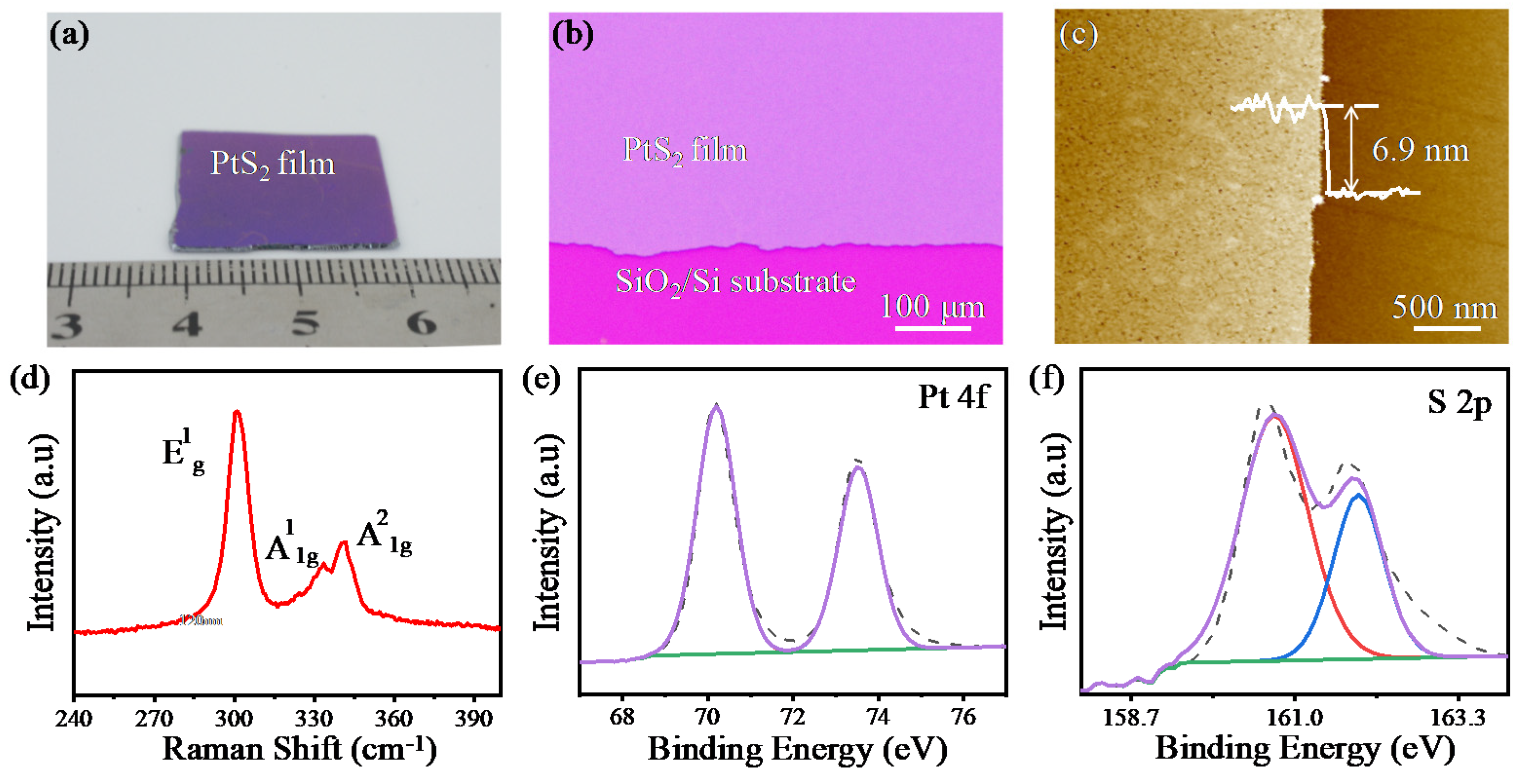
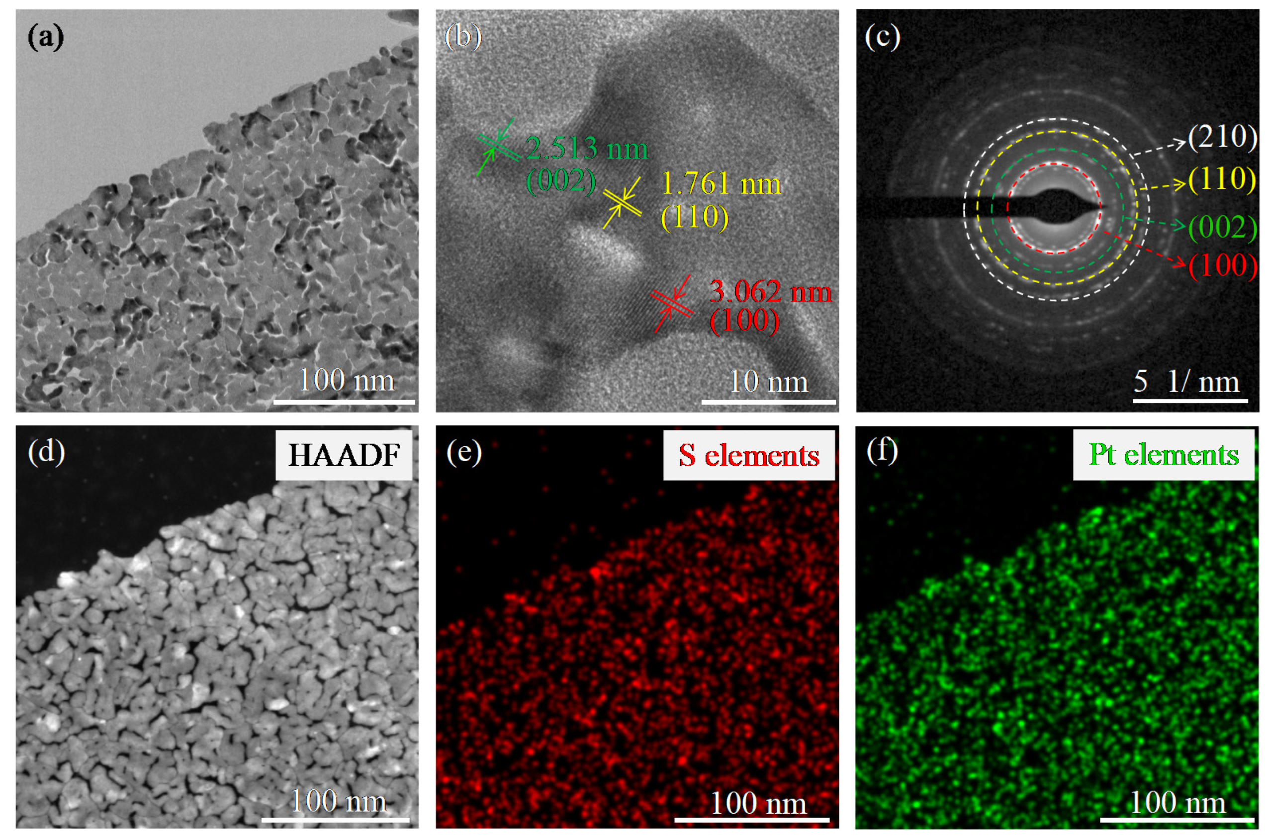
3.1. Crystal Structure and Characterizations of 2D PtS2

Figure 1a presents a photograph of large area PtS2 film deposited by CVD on a SiO2/Si substrate with a size larger than 4 cm2, prepared by the sulfuration of a platinum film with a thickness of about 3.03 nm. The optical microscope (OM) image of PtS2 film on the SiO2/Si substrate is shown in Figure 1b. The AFM image of the PtS2 film indicates a thickness of about 6.9 nm (Figure 1c). Raman spectra are shown in Figure 1d. Three characteristic peaks at 301, 334, and 341 cm−1 correspond to E1g, A1g, and A21g phonon modes, respectively [18]. The chemical state of the synthetic products after the sulfuration process was explored by high resolution XPS. For the Pt 4f orbital in Figure 1e, the binding energies of Pt 4f orbitals are approximately 70.1 and 73.5 eV, respectively, corresponding to Pt (IV) 4f 7/2 and 4f 5/2 orbitals [37]. As shown in Figure 1f, peaks at 160.7 and 161.7 eV contributed to the S elements with a chemical value of about −2. The results demonstrated that the Pt film completely reacted with sulfur gas and turned successfully into PtS2 film.
To further explore the crystalline structure of as-grown PtS2 films, HRTEM was carried out to investigate the refined grain boundary at the nanoscale. The large-area PtS2 films were transferred to the TEM grid. In Figure 2a,b, the HRTEM images of as-obtained PtS2 films show some cracks despite connecting at the large scale, contributing to the broken grain boundary in original films during the transfer process. Lattice spacing of 0.31 nm, 0.176 nm, and 0.251 nm is attributed to the (100), (110), and (002) planes of PtS2 crystal, respectively, as seen in Figure 2b. The diffraction rings from inside to outside can be readily assigned to (100), (002), (110), and (210) planes of PtS2 crystal (Figure 2c), proving that as-synthesized PtS2 films are polycrystalline. As shown in Figure 2d, high-angle annular dark field scanning transmission electron microscopy (HAADF-STEM) further confirms the homogeneity of PtS2 films. The EDS elemental mapping in Figure 2e,f demonstrates that Pt and S elements are uniformly distributed on the synthesized PtS2 films.

3.2. Photoelectric Transport Characteristic of PtS2 Films at Room Temperature

Back gate PtS2 film array FETs were fabricated on SiO2/Si substrate with an oxide layer thickness of about 300 nm to explore their R performances. The schematic of few layer PtS2 film FETs is shown in Figure 3a. The array of Cr/Au metals were deposited as source electrodes and drain electrodes with a thickness of 5/50 nm. Figure 3b illustrates linear, coincident, and symmetric output characteristic curves of PtS2 FETs with a thickness of about 6.9 nm under back-gated voltage from −60 to 60 V, indicating the typical semi-metal transport behavior of as-obtained PtS2 films. In Figure 3c, the transfer characteristic curves are parallel with different Vds, further confirming the metallic property of as-grown PtS2 films [38]. Figure 3d depicts the Iph of PtS2 FETs as a function of illumination time at different laser wavelengths from 532 to 2200 nm with Vds = 2.0 V. The value of Iph decreased as the illumination wavelength increased from 532 to 2200 nm, indicative of the changes in light absorption efficiency at different wavelengths. The photo-response of PtS2 FETs irradiated by a 1550 nm laser with different power densities is shown in Figure 3e. The photo-response of PtS2 FETs irradiated as a function of power densities under 532, 980, and 1850 nm laser is shown in Figure S2a–c (details in supporting information). The Iph increases as laser power increases. Proving that the synthesized PtS2 film is an excellent broad-spectrum infrared absorbing material [36,39]. PtS2 film FETs stability was evaluated in Figure 3f, by repeatedly switching the incident laser on/off every 20 s with a bias voltage of 2.0 V. The results reveal that the devices can perform reversible conversions between high and low conduction in the laser on/off status. One of the key parameters used to evaluate the performance of the photodetector is its response speed. The rise (τrise) and decay times (τdecay) of as-obtained PtS2 FETs are 0.18 and 0.2 s under 1550 nm laser illumination, respectively (Figure 3g). The τrise and τdecay of PtS2 FETs under 532, 980, and 1850 nm laser illumination are also shown in Figure S2d–f. The response and decay times are 0.16 and 0.26 s, 0.25 and 0.28 s, 0.29 and 0.27 s for the cases under 532, 980, and 1850 nm illumination, respectively. Figure 3h shows a function-related fitted plot based on the Iph and R of various incident light powers at 1550 nm illumination. The R was defined as the Iph generated per unit power of incident light on the channel area [40], R = Iph/P, where Iph is the photogenerated current and P is the optical power irradiated on the effective channel area. The R decreases as the optical power increases, and the maximum R of PtS2 FETs at 1550 nm is 3.20 A/W. The PtS2 FETs fit the image under the 532, 980, and 1850 nm lasers, as shown in Figure S2g–i. The results demonstrated that the R of PtS2 FETs are 3.55 A/W, 0.97 A/W, and 1.42 A/W, respectively. D* represents the detectivity per unit bandwidth and surface area. After ignoring Johnson noise, the D* is expressed as D* = RA1/2/(2eIdark)1/2, where A is the effective channel area [4]. The functional relationship between incident light power at 1550 nm and D* is illustrated in Figure 3i, with a maximum D* capability of 1.24 × 10⁷ Jones. Under 532, 980, and 1850 nm, Figure S2j–i (supporting information) depicts the functional relationship of the PtS2 device. The results demonstrate that the D* of PtS2 FETs are 1.35 × 10⁷ Jones, 3.83 × 10⁶ Jones, and 5.55 × 10⁷ Jones, respectively.

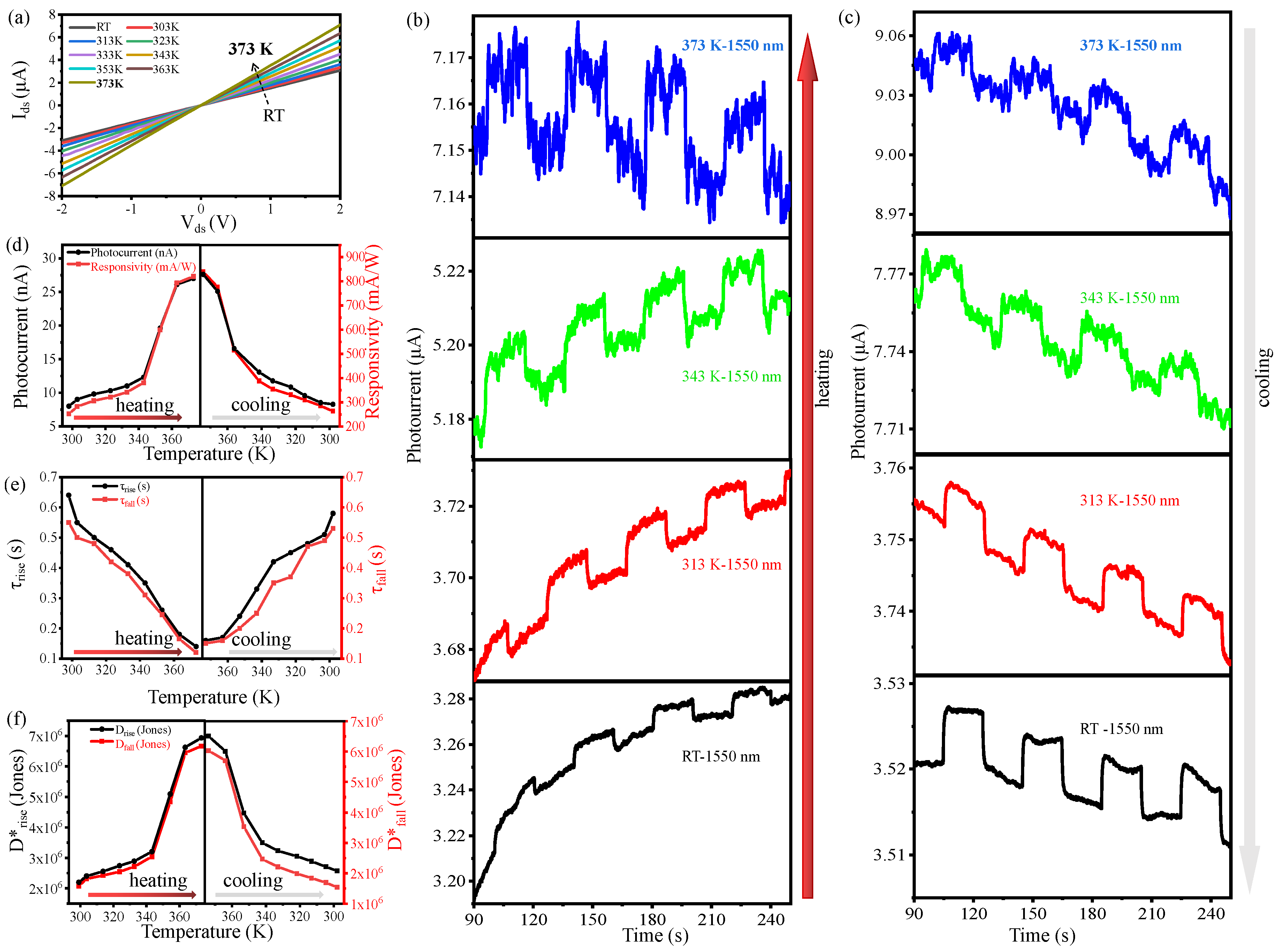
3.3. Photoelectric Transport Characteristic of PtS2 Film at High Temperature

To investigate the photoelectric properties of PtS2 at high temperatures, as-fabricated PtS2 FETs were heated and measurements were taken every 10 K on the photoelectric test platform until the Iph was weak and the temperature had reached its high restriction and was then cooled to room temperature every 10 K to observe changes in its wide spectra photo-response properties. Figure 4a shows the current-voltage (Ids-Vds) characteristic curves of PtS2 FETs as the working temperature increased from room temperature to 373 K at 1550 nm with Vds at 2 V. It can be seen that Ids increased as the temperature rose from room temperature to 373 K (limit temperature). Figure S3a shows the Ids-Vds characteristic curve of PtS2 FETs after it cooled from 373 K to room temperature. The photo-response of PtS2 FETs changed with the irradiation time of different laser wavelengths at Vds = 2 V when warmed to 373 K, as revealed in Figure S3b. To better detect the photo-response performance of PtS2 films at high temperatures, the temperature-dependent Iph were studied at Vds = 2 V and 1550 nm laser illumination. The Iph evolution of PtS2 FETs from room temperature to 373 K, and cooling from 373 K to room temperature, are shown in Figure S3c,d (supporting information), respectively. Figure 4b,c show the Iph as a function of illumination time curves when the working temperature was heated from room temperature to 373 K and cooled from 373 K to room temperature, respectively.
Both the dark current and Iph increased as the device heated up (Figure 4b). When the temperature was cooled down from the limiting temperature to room temperature, the dark current and Iph both decreased (Figure 4c). Figure 4d shows a correlated evolution of Iph and R during the working temperature heating up and cooling in the range from 373 K to room temperature under 1550 nm laser illumination. The τrise and τdecay are statistically analyzed to better understand the variation law of light response at different temperatures. The evolution of τrise and τdecay with different working temperatures are shown schematically in Figure 4e. It can be seen that as the working temperature increases, the τrise and τdecay both decrease. The evolution of D* at different working temperatures during the heating up and cooling process under 1550 nm laser illumination is shown in Figure 4f. The results show that as the temperature increases, the D* also increases, with the maximum D* up to 6.1 × 10⁶ Jones.

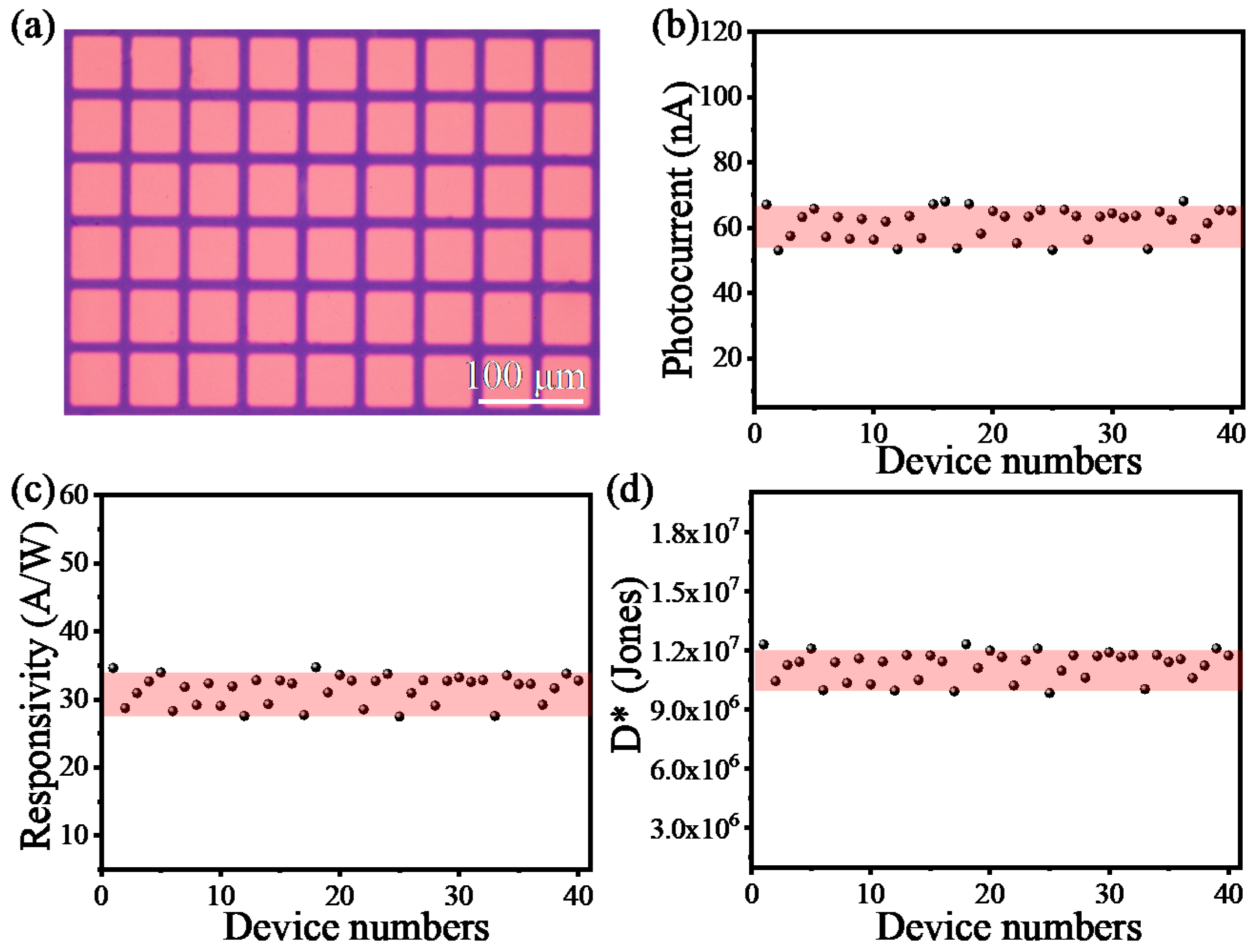
3.4. Characterization of Large Area Uniformity of PtS2 Films

To explore the photo-response uniformity of as-obtained PtS2 films, the array FETs were fabricated on large-area CVD-grown PtS2 films, and the 10.52 μm × 52.1 μm rectangular area between the source and drain is device channeled. The OM image is shown in Figure 5a. The PtS2 FETs were measured under 1550 nm laser illumination with Vds of about 2 V under air condition by 40 randomly selected electrodes. As shown in Figure 5b, the average value of statistical Iph is 61.4 nA, and the standard deviation is about 4.73 nA. Figure 5c,d shows the related R and D* of PtS2 array FETs. The average value of statistical R is 3.14 A/W; the standard deviation is 0.22 A/W. The average value of D* is 1.12 × 10⁷ Jones, and the standard deviation is 7.39 × 10⁵ Jones. The results show the high uniformity of as-fabricated PtS2 film FETs.

4. Discussion

High quality and large area platinum sulfide films were synthesized by CVD. The properties of platinum sulfide films at high temperature were investigated for the first time. As the temperature increased, both the absorption and number of photogenerated carriers increased as the Iph increased [41,42]. As a result, the photodetector R showed a trend to increase with temperature. Thus, the as-fabricated PtS2 photodetector is stable even at a high temperature of 373 K. The multiple photodetectors presented can be used for many applications where large surface area and high frequency are important.

5. Conclusions

In conclusion, a high-quality, large-area, two-dimensional PtS2 film was prepared on SiO2/Si substrate. The prepared PtS2 device achieved a broadband photo-response of 532–2200 nm, and a high D* response. Even when the PtS2 device was heated to 373 K, it still displayed excellent photo-response. In addition, as the temperature changed, the electrical and optical properties of the prepared FETs showed certain regularities. This research has opened up an interesting way to realize the application of large-area PtS2 devices, and is a potential candidate for new electronic devices.

Supplementary Materials

The following supporting information can be downloaded at: https://www.mdpi.com/article/10.3390/electronics11060838/s1, Figure S1. Pt AFM image plated on SiO2/Si substrate; Figure S2. Pho-to-response performance of PtS2 films based FETs at 532, 980, 1850 nm. (ac) Photo-response of the device under different wavelengths of laser illumination under 532, 980 and 1850 nm as the power density decreased. (df) Photo-response of the photodetector to on/off laser illumination is 532, 980, and 1850 nm, respectively. (gi) Photocurrent and responsivity as a function of laser il-lumination power density at 532, 980, and 1850 nm, respectively. (jk) The power of incident light at 532, 980, 1850 nm and the detectivity (D*) have a functional relationship, respectively; Figure S3. Photoelectric properties of PtS2 nanosheets at high temperature. (a) Room temperature output characteristic curve of PtS2 device 373 K. (b) The photocurrent changes at different laser wavelengths when the PtS2 FET is heated to 373 K, and Vds = 2 V. At Vds = 2.0 V, the optical re-sponse changes with temperature when the PtS2 device is heated to 373 K (c) and then reduced from 373 K to room temperature (d).

Author Contributions

Y.Z. and Q.F. contributed equally to this work. Conceptualization and Writing Original Draft, Y.Z. and Q.F. Investigation, R.H. Validation, M.Z. All authors have read and agreed to the published version of the manuscript.

Funding

This work is supported by the National Key Research and Development Program of China (2021YFA0717800), the Key Research and Development Program of Shaanxi Province (2021GY-217), the Research Funds for Interdisciplinary Subject of NWPU (19SH0304), the Fundamental Research Funds for the Central Universities (3102017jc01001).

Data Availability Statement

Not applicable.

Conflicts of Interest

The authors declare no conflict of interest.

References

  1. Liu, Z.J.; Chen, W. Space applications of staring imaging technology with area FPA. Infrared Laser Eng. 2006, 35, 541–545. [Google Scholar]
  2. Verdun, M.E.L.; Beaudoin, G.; Portier, B.; Bardou, N.; Dupuis, C.; Sagnes, I.; Haiedar, R.; Pardo, F.; Pelouard, J.L. Dark current investigation in thin P-i-N InGaAs photodiodes for nano-resonators. J. Appl. Phys. 2016, 120, 08451. [Google Scholar] [CrossRef] [Green Version]
  3. Sun, Z.; Chang, H. Graphene and graphene-like two-dimensional materials in photodetection: Mechanisms and methodology. ACS Nano 2014, 8, 4133–4156. [Google Scholar] [CrossRef] [PubMed]
  4. Buscema, M.; Island, J.O.; Groenendijk, D.J.; Blanter, S.I.; Steele, G.A.; Van der Zant, H.S.; Castellanos-Gomez, A. Phoocurrent generation with two-dimensional van der Waals semiconductors. Chem. Soc. Rev. 2015, 44, 3691–3718. [Google Scholar] [CrossRef] [PubMed] [Green Version]
  5. Li, J.; Niu, L.; Zheng, Z.; Yan, F. Photosensitive graphene transistors. Adv. Mater. 2014, 26, 5239–5273. [Google Scholar] [CrossRef]
  6. Martyniuk, P.; Rogalski, A. HOT infrared photodetectors. Opto-Electron. Rev. 2013, 21, 239–257. [Google Scholar] [CrossRef]
  7. Li, H.; Yin, Z.; He, Q.; Li, H.; Huang, X.; Lu, G.; Fam, D.W.H.; Tok, A.I.Y.; Zhang, Q.; Zhang, H. Fabrication of single-and multilayer MoS2 film-based field-effect transistors for sensing NO at room temperature. Small 2012, 8, 63–67. [Google Scholar] [CrossRef] [PubMed]
  8. Jiang, W.; Wang, X.; Chen, Y.; Wu, G.; Ba, K.; Xuan, N.; Sun, Y.; Gong, P.; Bao, J.; Shen, H. Large-area high quality PtSe2 thin film with versatile polarity. InfoMat 2019, 1, 260–267. [Google Scholar]
  9. Ye, M.; Zhang, D.; Yap, Y. Recent advances in electronic and optoelectronic devices based on two-dimensional transition metal dichalcogenides. Electronics 2017, 6, 43. [Google Scholar] [CrossRef] [Green Version]
  10. Bablich, A.; Kataria, S.; Lemme, M.C. Graphene and Two-Dimensional Materials for Optoelectronic Applications. Electronics 2016, 5, 13. [Google Scholar] [CrossRef] [Green Version]
  11. Kaushik, S.; Sorifi, S.; Singh, R. Study of temperature dependent behavior of h-BN nanoflakes based deep UV photodetector. Photonic Nanostruct. 2021, 43, 100887. [Google Scholar] [CrossRef]
  12. Jin, X.; Wu, Q.; Huang, S.; Deng, G.; Yao, J.; Huang, H.; Zhao, P.; Xu, J. High-performance black silicon photodetectors operating over a wide temperature range. Opt. Mater. 2021, 113, 110874. [Google Scholar] [CrossRef]
  13. Kochman, B.; Stiff-Roberts, A.D.; Chakrabarti, S.; Phillips, J.D.; Krishna, S.; Singh, J.; Bhattacharya, P. Absorption, carrier lifetime, and gain in InAs-GaAs quantum-dot infrared photodetectors. IEEE J. Quantum Electron. 2003, 39, 459–467. [Google Scholar] [CrossRef]
  14. Lee, H.; Chun, Y.T. Ferroelectric Induced UV Light-Responsive Memory Devices with Low Dark Current. Electronics 2021, 10, 1897. [Google Scholar] [CrossRef]
  15. Almayyali, A.O.M.; Kadhim, B.B.; Jappor, H.R. Tunable electronic and optical properties of 2D PtS2/MoS2 van der Waals heterostructure. Physica E 2020, 118, 113866. [Google Scholar] [CrossRef]
  16. Maimon, S.; Wicks, G. nBn detector, an infrared detector with reduced dark current and higher operating temperature. Appl. Phys. Lett. 2006, 89, 151109–151112. [Google Scholar] [CrossRef]
  17. Deviprasad, V.P.; Ghadi, H.; Das, D.; Panda, D.; Rawool, H.; Chavan, V.; Tongbram, B.; Patwari, J.; Pal, S.K.; Chakrabarti, S. High performance short wave infrared photodetector using p-i-p quantum dots (InAs/GaAs) validated with theoretically simulated model. J. Alloy Compd. 2019, 804, 18–26. [Google Scholar] [CrossRef]
  18. Gawron, W.; Damiecki, A.; Kozniewski, A.; Martyniuk, P.; Stasiewicz, K.A.; Madejczyk, P.; Rutkowski, J. Multiple Long Wavelength Infrared MOCVD Grown HgCdTe Photodetectors for High Temperature Conditions. IEEE Sens. J. 2021, 21, 4509–4516. [Google Scholar] [CrossRef]
  19. Liu, Y.; Ma, Y.; Li, X.; Gu, Y.; Li, T.; Wan, L.; Shao, X.; Gong, H. High Temperature Behaviors of 1–2.5 μm Extended Wavelength In0.83Ga0.17As Photodetectors on InP Substrate. IEEE J. Quantum Electron. 2021, 57, 400407. [Google Scholar] [CrossRef]
  20. Cheng, Z.; Cao, R.; Wei, K.; Yao, Y.; Liu, X.; Kang, J.; Dong, J.; Shi, Z.; Zhang, H.; Zhang, X. 2D Materials Enabled Next-Generation Integrated Optoelectronics: From Fabrication to Applications. Adv. Sci. 2021, 8, 2003834–2203855. [Google Scholar] [CrossRef]
  21. Zhao, Y.; Qiao, J.; Yu, P.; Hu, Z.; Lin, Z.; Lau, S.P.; Liu, Z.; Ji, W.; Chai, Y. Extraordinarily Strong Interlayer Interaction in 2D Layered PtS2. Adv. Mater. 2016, 28, 2399–2407. [Google Scholar] [CrossRef] [PubMed]
  22. Villaos, R.A.B.; Crisostomo, C.P.; Huang, Z.-Q.; Huang, S.-M.; Padama, A.A.B.; Albao, M.A.; Lin, H.; Chuang, F.-C. Thickness dependent electronic properties of Pt dichalcogenides. npj 2D Mater. Appl. 2019, 3, 2. [Google Scholar] [CrossRef] [Green Version]
  23. Nguyen, C.V.; Bui, H.D.; Nguyen, T.D.; Pham, K.D. Controlling electronic properties of PtS2/InSe van der Waals heterostructure via external electric field and vertical strain. Chem. Phys. Lett. 2019, 724, 1–7. [Google Scholar] [CrossRef]
  24. Du, J.; Song, P.; Fang, L.; Wang, T.; Wei, Z.; Li, J.; Xia, C. Elastic, electronic and optical properties of the two-dimensional PtX2 (X=S, Se, and Te) monolayer. Appl. Surf. Sci. 2018, 435, 476–482. [Google Scholar] [CrossRef]
  25. Chen, E.; Xu, W.; Chen, J.; Warner, J.H. 2D layered noble metal dichalcogenides (Pt, Pd, Se, S) for electronics and energy applications. Mater. Today Chem. 2020, 7, 100076. [Google Scholar] [CrossRef]
  26. Ji, Y.; Liu, Y.; Xu, Y.; Liu, L.; Chen, Y. Electronic and optical properties of sulfur vacancy-defect monolayer PtS2: A first-principles study. Mater. Chem. Phys. 2020, 255, 123588. [Google Scholar] [CrossRef]
  27. Zhang, W.; Huang, Z.; Zhang, W.; Li, Y. Two-dimensional semiconductors with possible high room temperature mobility. Nano Res. 2014, 7, 1731–1737. [Google Scholar] [CrossRef] [Green Version]
  28. Miró, P.; Ghorbani-Asl, M.; Heine, T. Two dimensional materials beyond MoS2: Noble-transition-metal dichalcogenides. Angew. Chem. Int. Ed. 2014, 53, 3015–3018. [Google Scholar] [CrossRef]
  29. Pi, L.; Li, L.; Hu, X.; Zhou, S.; Li, H.; Zhai, T. Temperature dependence of Raman responses of few-layer PtS2. Nanotechnology 2018, 29, 505709. [Google Scholar] [CrossRef]
  30. Late, D.J.; Shirodkar, S.N.; Waghmare, U.V.; Dravid, V.P.; Rao, C. Thermal expansion, anharmonicity and temperature-dependent Raman spectra of single-and few-layer MoSe2 and WSe2. Chemphyschem 2014, 15, 1592–1598. [Google Scholar] [CrossRef]
  31. Li, L.; Gong, P.; Wang, W.; Deng, B.; Pi, L.; Yu, J.; Zhou, X.; Shi, X.; Li, H.; Zhai, T. Strong in-plane anisotropies of optical and electrical response in layered dimetal chalcogenide. ACS Nano 2017, 11, 10264–10272. [Google Scholar] [CrossRef] [PubMed]
  32. Luo, S.; Qi, X.; Yao, H.; Ren, X.; Chen, Q.; Zhong, J. Temperature-dependent Raman responses of the vapor-deposited tin selenide ultrathin flakes. J. Phys. Chem. C 2017, 121, 4674–4679. [Google Scholar] [CrossRef]
  33. Pawbake, A.S.; Island, J.O.; Flores, E.; Ares, J.R.; Sanchez, C.; Ferrer, I.J.; Jadkar, S.R.; Van der Zant, H.S.; Castellanos-Gomez, A.; Late, D.J. Temperature-dependent Raman spectroscopy of titanium trisulfide (TiS3) nanoribbons and nanosheets. ACS Appl. Mater. Interfaces 2015, 7, 24185–24190. [Google Scholar] [CrossRef] [Green Version]
  34. Wang, Z.; Wang, P.; Wang, F.; Ye, J.; He, T.; Wu, F.; Peng, M.; Wu, P.; Chen, Y.; Zhong, F.; et al. A Noble Metal Dichalcogenide for High-Performance Field-Effect Transistors and Broadband Photodetectors. Adv. Funct. Mater. 2020, 30, 1907945. [Google Scholar] [CrossRef]
  35. Li, L.; Wang, W.; Chai, Y.; Li, H.; Tian, M.; Zhai, T. Few-Layered PtS2 phototransistor on h-BN with high gain. Adv. Funct. Mater. 2017, 27, 1701011. [Google Scholar] [CrossRef]
  36. Yuan, J.; Sun, T.; Hu, Z.; Yu, W.; Ma, W.; Zhang, K.; Sun, B.; Lau, S.P.; Bao, Q.; Lin, S.; et al. Wafer-Scale Fabrication of Two-Dimensional PtS2/PtSe2 Heterojunctions for Efficient and Broad band Photodetection. ACS Appl. Mater. Interfaces 2018, 10, 40614–40622. [Google Scholar] [CrossRef]
  37. Liu, J.; Xu, H.; Yan, J.; Huang, J.; Song, Y.; Deng, J.; Wu, J.; Ding, C.; Wu, X.; Yuan, S.; et al. Efficient photocatalytic hydrogen evolution mediated by defect-rich 1T-PtS2 atomic layer nanosheet modified mesoporous graphitic carbon nitride. J. Mater. Chem. A 2019, 7, 18906–18914. [Google Scholar] [CrossRef]
  38. Ma, H.; Qian, Q.; Qin, B.; Wan, Z.; Wu, R.; Zhao, B.; Zhang, H.; Zhang, Z.; Li, J.; Zhang, Z.; et al. Controlled Synthesis of Ultrathin PtSe2 Nanosheets with Thickness-Tunable Electrical and Magnetoelectrical Properties. Adv. Sci. 2022, 9, 2103507. [Google Scholar] [CrossRef]
  39. Wang, X.; Cheng, P.K.; Tang, C.Y.; Long, H.; Yuan, H.; Zeng, L.; Ma, S.; Qarony, W.; Tsang, Y.H. Laser Q-switching with PtS2 microflakes saturable absorber. Opt. Express 2018, 26, 13055–13060. [Google Scholar] [CrossRef] [Green Version]
  40. Xie, C.; Mak, C.; Tao, X.; Yan, F. Photodetectors based on two-dimensional layered materials beyond graphene. Adv. Funct. Mater. 2017, 27, 1603886. [Google Scholar] [CrossRef]
  41. Sorifi, S.; Moun, M.; Kaushik, S.; Singh, R. High-Temperature Performance of a GaSe Nanosheet-Based Broadband Photodetector. ACS Appl. Electron. Mater. 2020, 2, 670–676. [Google Scholar] [CrossRef]
  42. Chen, B.; Yang, Y.; Xie, X.; Wang, N.; Ma, Z.; Song, K.; Zhang, X. Analysis of temperature-dependent characteristics of a 4H-SiC metal-semiconductor-metal ultraviolet photodetector. Chin. Sci. Bull. 2012, 57, 4427–4433. [Google Scholar] [CrossRef] [Green Version]
Figure 1. Characterization of continuous PtS2 films. (ac) Photograph, OM, and AFM images of CVD-grown PtS2 continuous film, respectively. (df) Raman spectra and high resolution XPS spectra of Pt and S elements of as-obtained large-area PtS2 film.
Electronics 11 00838 g001
Figure 2. Characterization of crystal structure and quality of as-grown PtS2 films. (a,b) HRTEM image of PtS2 films. (c) The corresponding selected area electron diffraction pattern of PtS2 film. (d) HAADF-STEM image of PtS2 films. (e,f) EDS elemental mapping images of PtS2 film.
Electronics 11 00838 g002
Figure 3. Optoelectrical properties of as-grown PtS2 films at room temperature. (a) Schematic of back gate PtS2 FETs on SiO2/Si substrate. (b,c) Output and transfer characteristics of PtS2 FETs under room temperature and air conditioning. (d) Iph of PtS2 film FETs with Vds = 2 V and various laser wavelengths from 532 nm to 2200 nm. (e) Photo-response at wavelength of 1550 nm with power density ranging from 0.01 to 0.18 μW. (f) The Iph response to on/off laser illumination at 1550 nm. (g) The response time of PtS2 FETs at 1550 nm. τrise is the rise time when the net Iph increases from 10% to 90%. τdecay is the decay time when the net Iph decreases from 90% to 10%. (h,i) Iph and D* as a function of laser power at 1500 nm, respectively.
Electronics 11 00838 g003
Figure 4. Temperature-dependent photoelectric properties of PtS2 films. (a) Ids-Vds characteristic curve of PtS2 FETs when heating up from room temperature to 373 K. (b,c) Iph as a function of illumination time at 1550 nm during the heating up and cooling process from 373 K to room temperature at several selected points. (df) Iph and R (d), τrise and τdecay (e), D* (f) of PtS2 FETs at 1550 nm during the heating up and cooling from 373 K to room temperature.
Electronics 11 00838 g004
Figure 5. Large area uniformity of PtS2 array FETs. (a) The OM image of PtS2 array FETs on SiO2/Si substrate. (bd) Statistical Iph (b), R (c), and D* (d) of PtS2 array FETs at 40 randomly selected electrodes under 1550 nm laser illumination in air conditioning with Vds = 2.0 V.
Electronics 11 00838 g005
Publisher’s Note: MDPI stays neutral with regard to jurisdictional claims in published maps and institutional affiliations.

