Abstract
A millimeter-wave direct-conversion radio-frequency (RF) transmitter requires precise in-/quadrature-phase (I/Q) mismatch calibration and dc offset cancellation to minimize image rejection ratio (IRR) and LO feedthrough (LOFT) for ensuring satisfactory output spectral purity. We present a 28-GHz CMOS RF transmitter with an improved calibration technique for fifth generation (5G) wireless communication applications. The RF transmitter comprises a baseband amplifier, quadrature up-conversion mixer, power amplifier driver, and quadrature LO generator. The I/Q amplitude mismatch is calibrated by tuning the gate biases of the switching stage FETs of the mixer, the I/Q phase mismatch is calibrated by tuning the varactor capacitances at the LC load of LO buffer, and the dc offset is cancelled by tuning the body voltages of the differential-pair FETs at the baseband amplifier. The proposed technique provides precise calibration accuracy by employing mV-resolution tuning voltage generation via 6-bit voltage digital-to-analog converters. It also covers wide calibration range while minimizing the impact on the circuit’s bias point and dissipated current during calibration. Implemented in a 65 nm CMOS process, the RF transmitter integrated circuit shows output-referred 1 dB compression power of +6.5 dBm, saturated output power of +12.6 dBm, and an operating band of 27.5–29.3 GHz while demonstrating satisfactory performances of −55.9 dBc of IRR and −36.8 dBc of LOFT.
1. Introduction
The fifth generation (5G) radio access technology is opening unprecedented wide utilization of millimeter-wave (mm-wave) bands in wireless communications. Compared to the conventional sub-6 GHz band (also referred to as the frequency range 1: FR1), the mm-wave frequency band (referred to as the frequency range 2: FR2) can effectively provide wide channel bandwidth to ensure the required high data rate for the enhanced mobile broadband communication services. According to the 5G new radio (NR) standard [1], several FR2 bands are assigned in the K-band, Ka-band, and V-band. More particularly, the 24–29 GHz, 37–43 GHz, and 47–48 GHz bands are assigned to total six bands that are numbered between n257 and n262. Among them, the n261 band of 27.5–28.35 GHz is one of the most widely utilized bands worldwide. This leads to the rising demand of cost-effective and seamless adoption of the 28-GHz mm-wave wireless functionality into the existing RF transceivers. For realizing a low-power low-complexity small-form-factor mm-wave RF transceiver, while maintaining the legacy sub-6 GHz functionality unaffected, CMOS realization of a 28 GHz RF transmitter and receiver is regarded as the most viable approach [2]. It can guarantee flexible and seamless co-integration of the new mm-wave and existing RF transceivers in a single chip. As part of such an effort, a CMOS design of a 28-GHz RF transmitter integrated circuit (IC) is presented in this work.
For the CMOS design of a mm-wave RF transmitter, two performance parameters are considered the most critical: the output power and error vector magnitude (EVM). Nevertheless, it should be pointed out that the output power requirement can be relaxed to some extent. This is because typical output power that can be achieved from a CMOS power amplifier is only 10–20 dBm in the millimeter-wave band [3], and, thus, an additional GaAs power amplifier is almost always needed to boost the output power further up to the typically required 30–35 dBm by 5G. In contrast, there is not much room for tolerating the EVM degradation. The quadrature amplitude modulation (QAM) is usually utilized in 28-GHz 5G communications for a high data rate. To make the multiple-amplitude and multiple-phase QAM signal clear and clean, low EVM must be guaranteed for satisfactory signal-to-noise-and-distortion ratio (SNDR) in the RF transmitter. During the circuit simulation process of a CMOS RF transmitter, the EVM and SNDR are usually evaluated in an indirect way such that the image rejection ratio (IRR) and LO feedthrough rejection (LOFT) are under a single-tone driving condition, which is then translated to the SNDR and EVM according to the adopted QAM complexity such as 16- or 64-QAM.
Previous mm-wave CMOS RF transmitters were reported in 24 GHz [4], 28 GHz [2], 45 GHz [5], 60 GHz [6], and 78 GHz [7], and demonstrated decent levels of IRR and LOFT performances of about −40 dBc. Note that such performances were possibly achieved by adopting calibration techniques in the RF circuits [2,5,6,7]. Even though a carefully balanced circuit and layout design without calibration would produce satisfactory performance to some extent as claimed in [4], it would not be possible to maintain such good IRR and LOFT performances only by design against the harsh process non-uniformity and variation conditions in modern sub-micron CMOS processes. Furthermore, it should be also noted that the good IRR and LOFT performances are only required by a direct-conversion transmitter. If the RF transmitter is designed in a heterodyne architecture with a high intermediate frequency (IF), the IRR and LOFT performances will not be governed by the mm-wave transmitter performing a double-sideband frequency up-conversion, but by the IF transmitter performing the single-sideband quadrature up-conversion. That is why some previous heterodyne CMOS transmitters such as [8,9,10,11] have not addressed the IRR and LOFT issue.
In this work, we present a CMOS design of a 28 GHz direct-conversion RF transmitter with an improved calibration technique for the I/Q mismatch and dc offset. Part of the preliminary design result of this transmitter can be found in author’s prior presentation [12]. Compared to the previous works [2,5,6,7], the proposed calibration technique proves to be more precise and power-efficient, while covering a wider mismatch range. The proposed calibration techniques should be instrumental in realizing a single-chip mm-wave CMOS RF transmitter for 5G wireless applications.
2. Design
2.1. Architecture
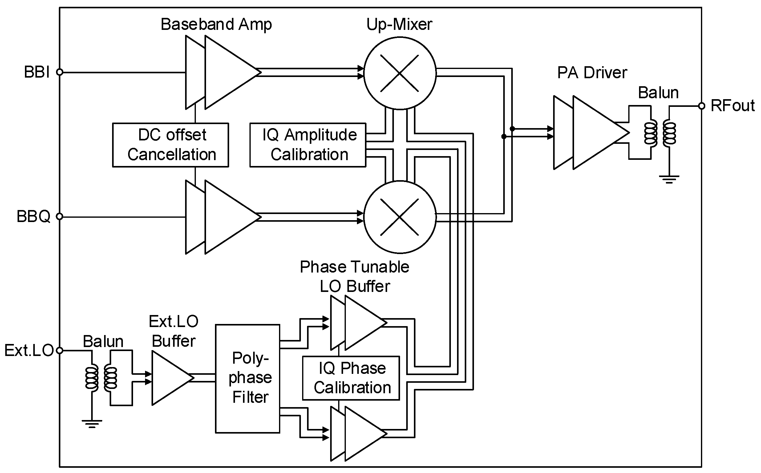
Figure 1 shows the architecture of the 28 GHz CMOS RF transmitter. It is based on the zero-IF direct quadrature up-conversion architecture. The single-ended I/Q baseband signals BBI and BBQ are fed to the single-to-differential baseband amplifier. The baseband amplifier also performs the DC offset cancellation (DCOC) for minimizing the LOFT. The quadrature mixer performs the single-sideband quadrature up-conversion mixing with the I/Q amplitude mismatch calibration. The quadrature output signal from the mixer is combined for image rejection and fed to the power amplifier driver. Assuming that an external high-power amplifier is connected at the driver amplifier to further boost the output power, the on-chip driver amplifier is designed to produce +6 dBm linear and +10 dBm saturated output power. It is a two-stage pseudo-differential pair structure with transformer coupling at the input and inter-stage and a transformer balun at the output for creating a single-ended 28-GHz output signal.

Figure 1.
The 28-GHz direct-conversion RF transmitter architecture.
For the quadrature local oscillator (LO) signal generation, a single-ended external LO signal is fed to a transformer balun first for the single-to-differential conversion, and subsequently to an external-LO buffer (ExtLO buffer in Figure 1) for compensating the balun-induced loss. The RC-CR polyphase filter converts the single-phase LO signal to the quadrature-phase I/Q LO signals. The final phase-tunable LO buffers boost the LO swing sufficiently large enough to drive the mixer, while performing the I/Q phase mismatch calibration.
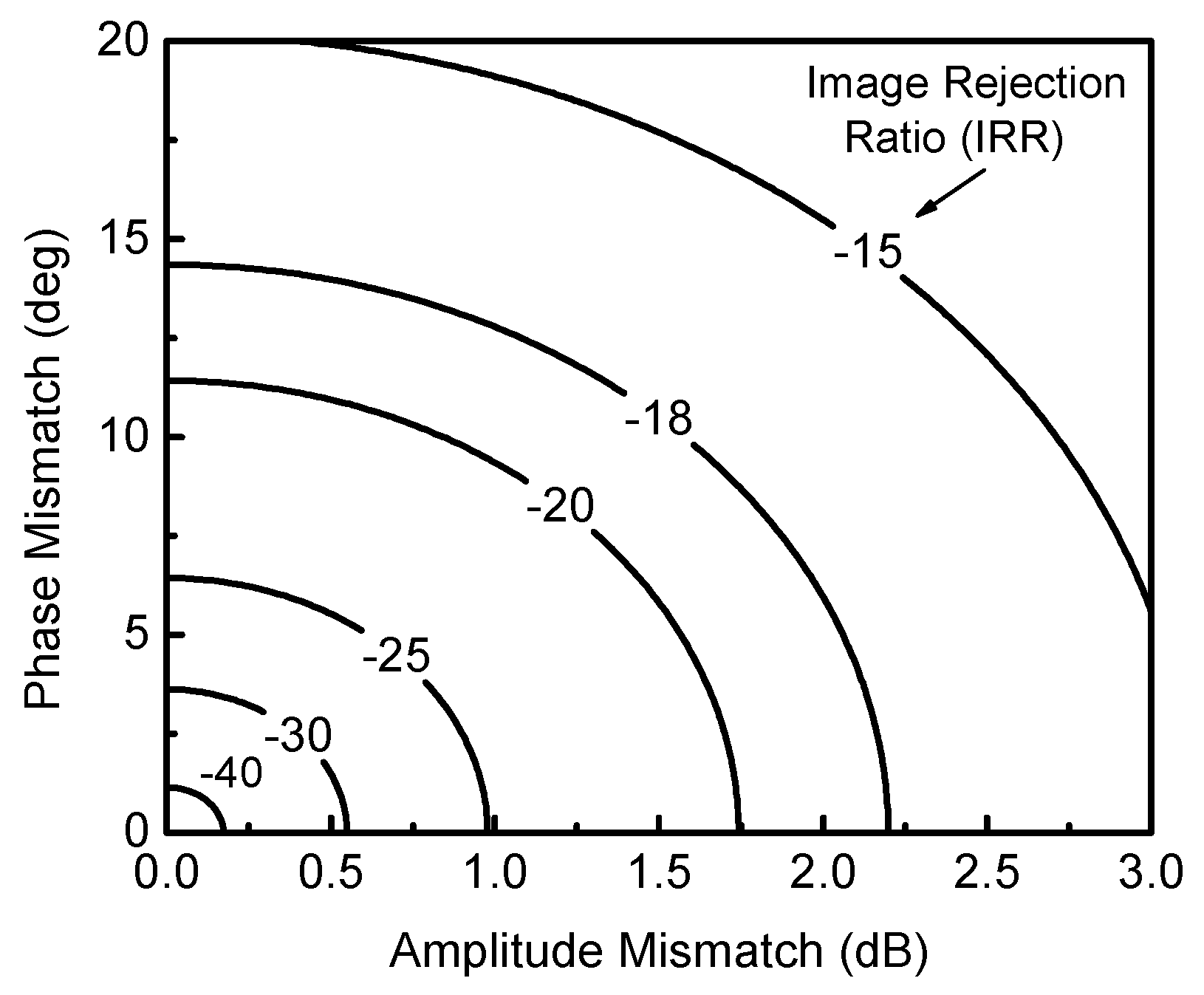
Before we discuss further on the details of the circuit design, let us examine the relation of the I/Q mismatch and IRR. A design guidance to the required accuracy and range for the mismatch calibration will be understood through this discussion. Let us assume that the baseband I/Q signals, and , and the LO I/Q signals, and , are expressed as follows,
where , , , and are the amplitudes and frequencies of the baseband and LO signals, respectively. Note that the I/Q mismatch is modeled in the baseband signal of (2) by the two parameters of the amplitude mismatch and the phase mismatch , whereas perfect I/Q matching is assumed for the LO signal. By computing the quadrature mixing operation by (1)–(4), the wanted RF component and unwanted image component are written as
Then, the IRR is given by the ratio of (5) and (6) as follows,
Figure 2 plots a two-dimensional contour graph of the theoretical IRR of (7) with respect to the amplitude and phase mismatches and . We can clearly observe that both the amplitude and phase mismatches need to be improved together for lowering the IRR, whereas only a single parameter improvement cannot create significant improvement for the IRR. For rough estimations, a phase mismatch of 9 degrees and amplitude mismatch of 1.1 dB are needed for −20 dB of IRR. If we want to improve the IRR to −30 dB, phase and amplitude mismatches of 2.5 degrees and 0.4 dB are required. If we further improve the IRR to −40 dB, the phase and amplitude mismatches must be managed better than 1 degree and 0.1 dB. Knowing that the IRR without the calibration is typically 15–18 dBc, we can set the design goals for the I/Q mismatch calibration from these observations. It must guarantee better than 0.1-dB accuracy over 2.5-dB mismatch range for the I/Q amplitude imbalance, and 1-degree accuracy over 15-degree mismatch range for the I/Q phase imbalance.
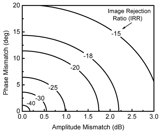
Figure 2.
Theoretical image rejection ratio (IRR) with respect to the I/Q amplitude and phase mismatches.
2.2. Up-Conversion Mixer Path and Amplitude Mismatch Calibration
As shown in Figure 1, the up-conversion mixer path comprises the baseband amplifier with dc offset cancellation, up-conversion mixer with I/Q amplitude mismatch calibration, and the driver amplifier. As discussed above for achieving better than −40 dBc of IRR, the I/Q amplitude mismatch calibration should ensure better than 0.1 dB accuracy covering over 2.5 dB mismatch range. A novel amplitude mismatch calibration technique that is improved compared to conventional ones is designed in this work.
One of the most straightforward calibration methods is to adjust the digital baseband signal fed from a preceding digital modem [13]. It however would not be a favorable approach considering that it always needs to work with a modem and cannot be functional with the RF transmitter alone. In contrast, analog domain calibration can be realized in the RF transmitter circuit so that it works on its own without a collaborating modem. The most popular approach for this is to tune the resistor–capacitor (RC) elements in a feedback path of a baseband amplifier. This is found a very popular approach in conventional RF transmitters having a narrow channel bandwidth such as, for example, a few MHz for sub-6 GHz applications [14,15] or at most a few hundred MHz for 5G applications [2]. However, since millimeter-wave RF transmitters desirably have a channel bandwidth over 1 GHz [1], the feedback-type baseband amplifier should not be appropriate because the complex switched-element feedback network induces huge parasitic elements and makes it difficult to increase the bandwidth over 1 GHz. Therefore, an open-loop-structure baseband amplifier with a direct transconductance (gm) control is more popular in wideband millimeter-wave RF transmitters [16,17]. The direct-gm control can be realized by tuning the bias current [6,18], tuning the core FET’s aspect ratio (W/L) [16], or properly interpolating I/Q gain stages [5]. Although found effective, this gm-control method usually induces huge changes of the dc bias current and operating point, which can lead to unwanted alteration of the FET’s operating condition, parasitic components and interfacing impedances, consequently resulting in unacceptable performance degradation.
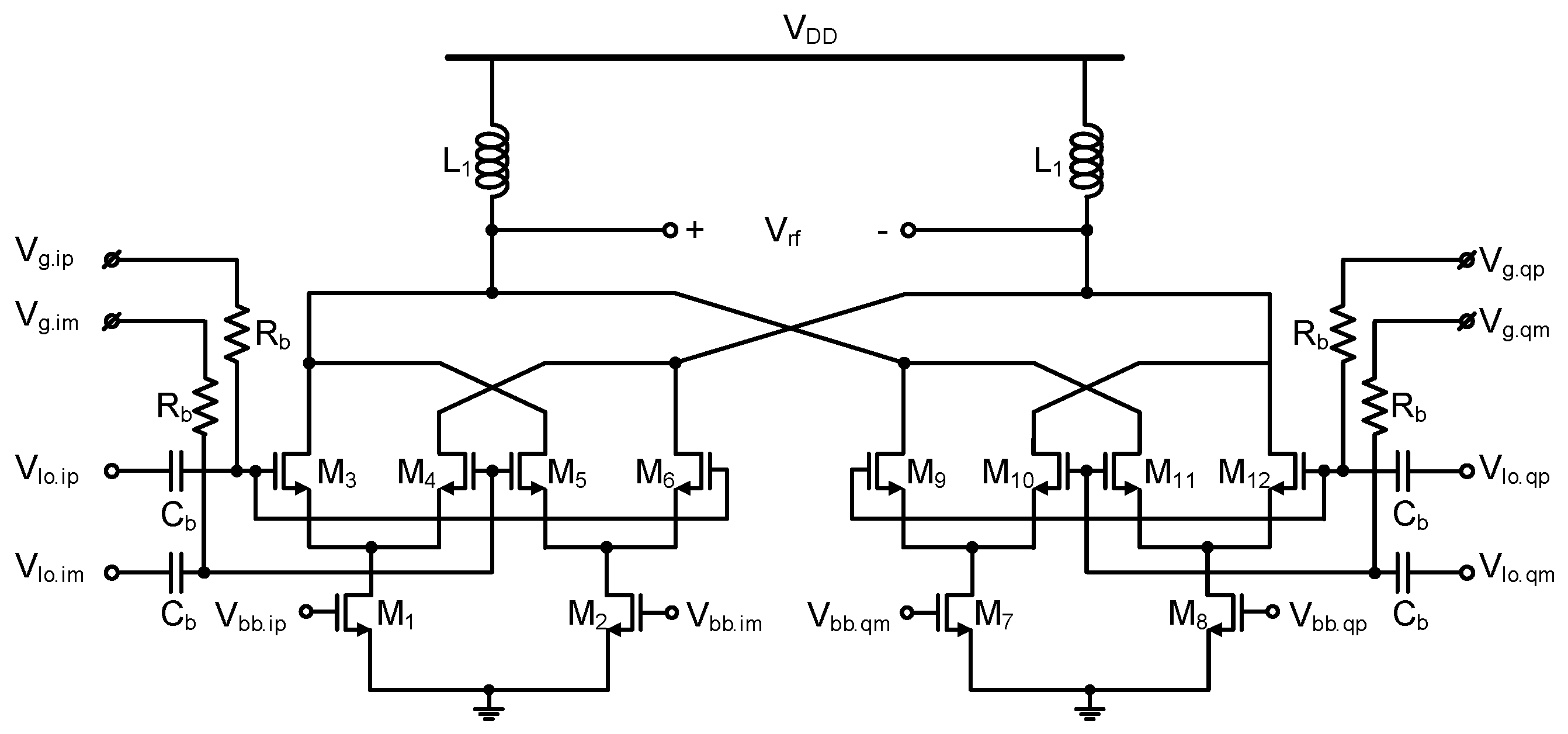
Compared to the conventional methods, we present an improved I/Q amplitude mismatch calibration technique. It completely avoids the issues originating from the conventional direct-gm control at the baseband amplifier, and proves to be precise, efficient, and robust. Figure 3 shows the quadrature up-conversion mixer schematic. It is a double-balanced Gilbert-cell structure. The I-path mixer M1–6 and the Q-path mixer M7–12 perform the frequency up-conversion by mixing the I/Q-path baseband signals Vbb,i and Vbb,q and the I/Q-path LO signals Vlo,i and Vbb,q, respectively. The I/Q-path output signals are added by the load inductor L1 (210 pH), producing a single-sideband RF output Vrf. The voltage gain of the mixer is +6 dB with the total current dissipation of 12 mA. The LO signals are ac-coupled through Cb, and their gate bias voltages Vg,ip, Vg,im, Vg,qp, and Vg,qm to the switching stage FETs M3–6 and M9–12 are independently fed through the ac-blocking resistor Rb (1 kΩ).
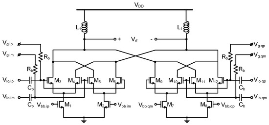
Figure 3.
Quadrature mixer schematic.
The I/Q amplitude mismatch is calibrated by controlling the switching-stage FETs’ gate biases. Controlling the gate biases Vg,ip, Vg,im, Vg,qp, and Vg,qm of the switching-stage FETs M3–6 and M9,10 causes alteration in the effective duty cycle of the LO signal that is arrived at the switching FETs’ gate nodes, which in turn affect the conversion gain. In addition, this method changes the transconductance and output resistance of the transconductance-stage FETs M1,2 and M7,8, which also affect the conversion gain. As a result, this method can ensure effective control of the I/Q signal amplitudes at the mixer output.
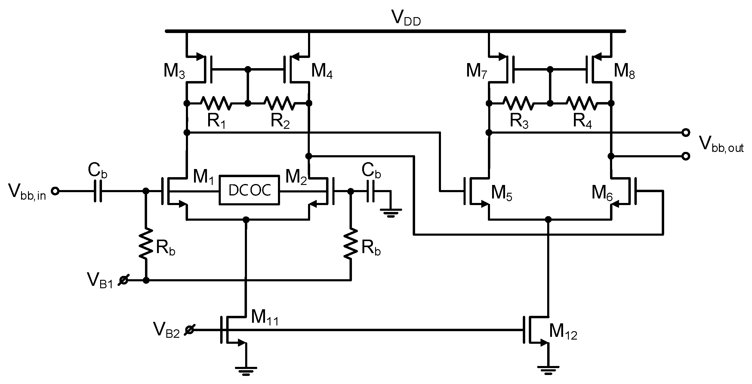
Before we further describe the I/Q amplitude mismatch calibration, let us first discuss on the dc offset cancellation at the baseband amplifier. The baseband amplifier preceding the mixer of Figure 3 is used to feed the baseband signal Vbb,i and Vbb,q to the mixer’s gm-stage M1,2 and M7,8. The schematic of the two-stage baseband amplifier is shown in Figure 4. It accepts the single-ended external input signal Vbb,in, converts it to differential with 10-dB amplification, and finally transfers the output signal Vbb,out to the mixer’s gm-stage. Simulations show that the 3-dB bandwidth is 10 MHz to 2.4 GHz, ensuring much wider than the wanted 1-GHz, and the differential mismatch induced during the single-to-differential conversion is only 0.01 dB and 0.02 degrees up to 1 GHz. Nevertheless, unwanted process non-uniformity and device mismatch can cause the dc offset at the output. In this design, the dc offset is cancelled by controlling the body bias voltage of the first-stage differential pair M1,2 [17]. This technique is found more advantageous than the conventional method of directly controlling the gate bias voltages of M1,2 and M3,4. It can decouple the dc offset cancellation condition and optimal gate bias condition to some extent, and thus allow the finding of the best optimal dc offset cancellation condition while minimally disturbing the dc bias condition. Due to this advantage, this technique was adopted in the author’s previous sub-6 GHz CMOS transceiver designs [19,20]. The body bias voltage is precisely generated by a 6-bit voltage digital-to-analog converter (VDAC). Since the same structure of VDAC is also adopted in the I/Q amplitude mismatch calibration, more details of the VDAC will be described next regarding the I/Q amplitude mismatch calibration.
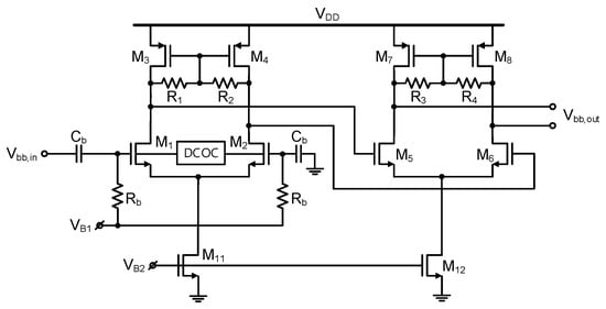
Figure 4.
Baseband amplifier schematic.
Figure 5 shows the VDAC schematic that is used to control the mixer’s gate bias voltage Vg,ip, Vg,im, Vg,qp, and Vg,qm of Figure 3. As mentioned earlier, the same VDAC is also adopted for the body bias voltage generator of Figure 4 except that the specific design values are differently set for its purpose. The VDAC comprises a full-scale generator and R-2R DAC. The full-scale generator sets the full scale of the R-2R DAC. It tunes the R2 and R3 between 0 and 16 kΩ in 3-bit 2-kΩ resolution so that the high- and low-ends of the full scale, Vgh and Vgl are set between 500 and 900 mV, while their difference |Vgh − Vgl| is fixed at a constant value of 50 mV. The subsequent R-2R DAC then generates the four output voltages with a fine resolution of 0.78 mV.
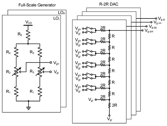
Figure 5.
Voltage digital-to-analog converter (VDAC) schematic.
To examine the effect of the proposed gate bias tuning method on the amplitude and phase of the mixer’s output signal, simulations are carried out for a unit Gilbert-cell mixer. Figure 6a is the schematic that is identical to the single-path of the original quadrature mixer shown in Figure 3. The baseband signal of 600 MHz and −20 dBm, and LO signal of 27.4 GHz and 0 dBm are applied, and the resulting RF output signal appears at 28 GHz with −14 dBm. For this simulation, Vg,p is swept from 0.45 to 1.05 V, while the Vg,m is fixed at a nominal value of 0.75 V. Thus, when both Vg,p and Vg,m are the same at 0.75 V, the mixer is in a perfect balanced condition, which is denoted as the point ‘A’ in Figure 6b. Away from this balanced point, the relative change of the amplitude and phase of the differential output signal Vrf of Figure 6a are plotted in Figure 6b. As can be seen, the amplitude changes by about 3.5 dB, and the phase changes by about 3 degrees with respect to the balanced point A. To evaluate how these changes can improve the IRR, this is projected to Figure 2 and translated to a rough estimation of the IRR improvement. If the initial IRR is assumed to be 18 dB without any calibration, the 3.5-dB amplitude change can sufficiently improve the IRR to better than −40 dBc. Meanwhile, it must be also noted that the accompanying 3-degree phase change makes a lot less impact on the IRR. The 3-degree phase tuning improves the IRR from −18 to −20 dBc, only by 2 dB, which is not sufficient to improve the IRR at all. Consequently, we conclude that the proposed gate bias tuning method covers a sufficiently wide range for the amplitude mismatch calibration while imposing a negligible impact on the phase.
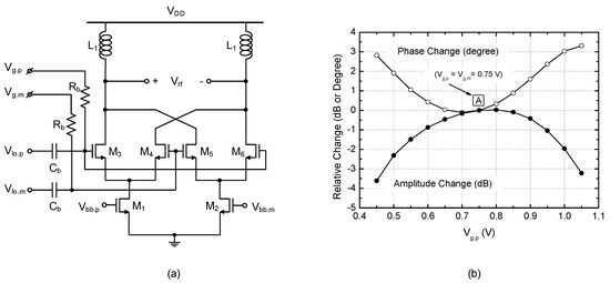
Figure 6.
Effect of the gate bias voltage control on the output signal in a single Gilbert-cell mixer. (a) Schematic; (b) Relative change of the amplitude and phase at the mixer’s output signal with respect to the gate bias voltage of the switching FET.
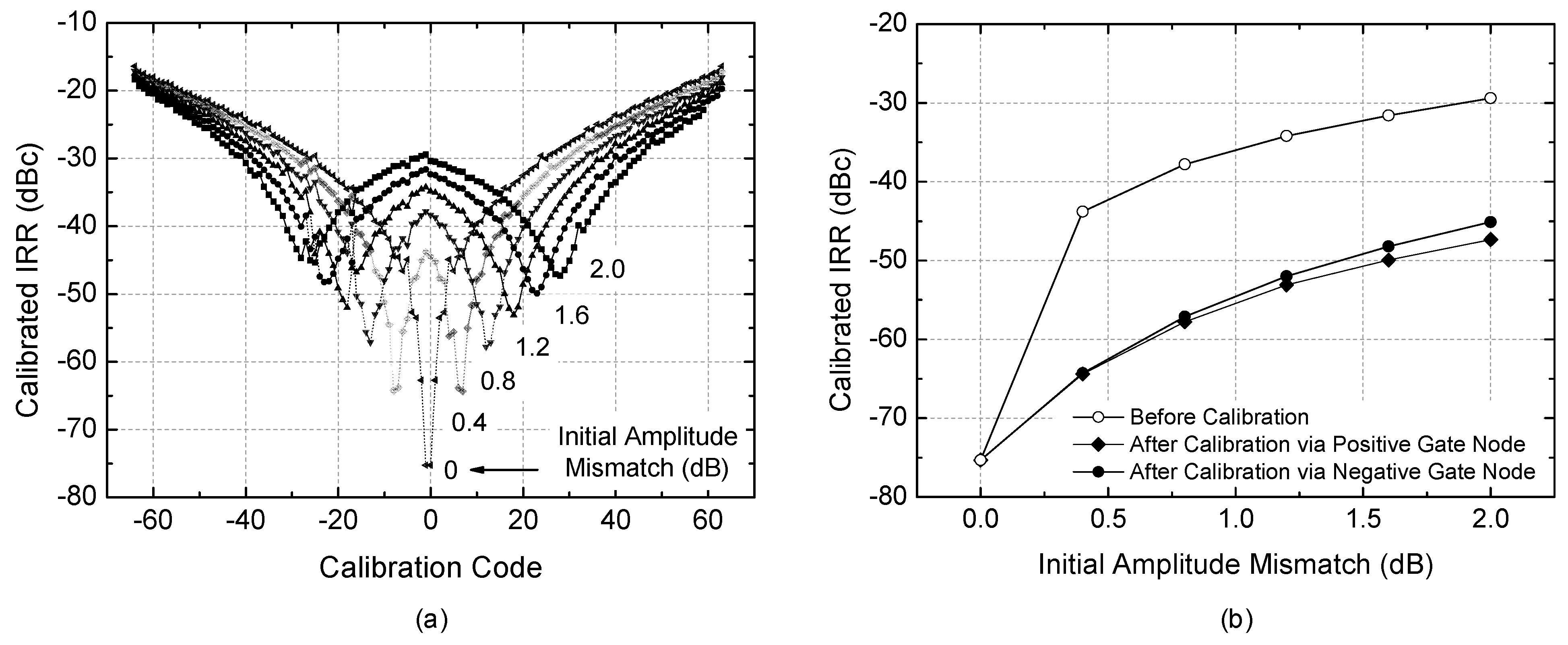
The proposed I/Q amplitude mismatch calibration is verified in simulation for the entire mixer of Figure 3. To clearly demonstrate the calibration effect, we intentionally introduce the I/Q amplitude mismatch by setting the I/Q amplitudes differently by 0–2 dB. The 6-bit calibration code is swept to see how the IRR is affected, and the results are plotted in Figure 7a. The first observation we can make is that when the mixer is in the perfect balanced condition with the initial amplitude mismatch = 0 dB, the natural IRR without any calibration (calibration code = 0) shows the best performance of −75 dBc. Then, as the amplitude mismatch is sequentially increased from 0.4 dB to 2.0 dB with 0.4 dB steps, the natural IRR without calibration (calibration code = 0) significantly degrades to −43–−29 dBc. However, when the 6-bit calibration code is properly adjusted, this natural IRR improves significantly. For example, when the initial amplitude mismatch is 1.2 dB, the natural IRR is only −34 dBc before calibration (calibration code = 0), and it significantly improves to −53 dBc after the calibration (calibration code = 18).
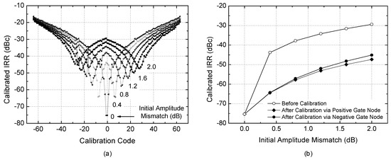
Figure 7.
Simulated I/Q amplitude mismatch calibration. (a) IRR calibration behavior with respect to the calibration code. (b) Comparison of the calibrated and uncalibrated IRR with respect to the initial amplitude mismatch.
Figure 7a also shows that the calibration effect is almost symmetric for the negative value of the code too. The polarity of the code in this simulation indicates that it tunes either the negative node voltages Vg,im or Vg,qm, or the positive node voltages Vg,ip or Vg,qp between the two differential nodes. This symmetric effect with respect to both polarities can be understood by considering that the Gilbert-cell mixer is a double-balanced structure, hence, tuning any polarity between the two differential LO gate nodes should not impose any difference on the output signal from the circuit structure point-of-view. Similar phenomena can be also observed in Figure 6b.
Figure 7b compares the natural IRR before the calibration and the best IRR after the calibration. As can be seen, the proposed technique successfully improves the IRR by 16–21 dB, leading to better than −45 dBc of IRR at any condition.
2.3. LO Generation Path and Phase Mismatch Calibration
As shown in Figure 1, the LO generation circuit comprises the balun, external-LO buffer, RC-CR polyphase filter, and phase-tunable LO buffer. It assumes that although not integrated in this transmitter, a single-phase VCO drives the RC-CR polyphase filter to generate quadrature LO signal. Note that the polyphase filter will not be needed if a quadrature VCO (QVCO) is employed as in 28 GHz [2] and 60 GHz [21]. In such a structure, the quadrature phase calibration can be done by tuning the tank capacitors in a quadrature VCO (QVCO). However, due to the complex coupling nature between the two VCO cores, the phase calibration would not be as effective, wide-range, and robust as we want. Therefore, we adopt the single-phase VCO in this work. In this structure adopting the single-phase VCO and polyphase filter, it is possible to perform the quadrature phase calibration by tuning the capacitors in the RC-CR polyphase filter [7]. However, due to the inherently narrow-band characteristics of the single-stage RC-CR filter, the phase tuning range is found very limited (only 3 degrees in [7]). Thus, this technique is not adopted in this work either. Another possible technique for the phase calibration is to interpolate the I and Q LO signals with proper weighting factors. It was demonstrated in a 45 GHz RF transmitter [5]. However, due to the rather complex circuit structure, it introduces large parasitic elements and thus the tuning range is very limited. Thus, this technique is found to be not as effective in mm-wave band as in the sub-6 GHz [5,22,23,24] either.
In this design, the phase calibration is carried out by the phase-tunable LO buffer. Figure 8 shows the schematic of the phase-tunable LO buffer. It is a two-stage differential amplifier in which the first stage is fully-differential and the second stage is pseudo-differential, with the two stages coupled via the transformer TF. Conventionally, the output phase of this circuit was tuned by the controlling bias current [25]. Thus, controlling VG1 of the tail current source FET M3 can tune the output phase. However, since the huge variation of the bias current also leads to huge variations of the bias condition, node impedance, and signal swing, we find this approach not effective. In this work, we choose to tune the load capacitor at the first stage. A similar approach can be found in a 24 GHz LO generation circuit [26], but their phase tuning range was only 4 degrees, which was too small for our target. Considering the discussions regarding Figure 2, we need the phase tuning range of at least over 15 degrees.
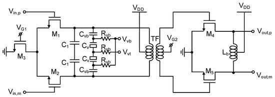
Figure 8.
Phase-tunable LO buffer schematic.
To achieve the wide and precise tunability, a MOS varactor is employed at the first-stage LC load. As can be seen in Figure 8, the load capacitor comprises a fixed capacitor C1 of 61 fF and a tunable varactor capacitor Cv of 46–77 fF. The inter-stage transformer TF is designed as a rectangular single-turn stacked structure with a dimension of 160 × 70 μm2. The two stacked layers are realized by the two top metal layers of metal 9 and 8 with thicknesses of 3.4 and 0.9 μm, respectively, and their spacing of 0.75 μm. Electromagnetic simulation verifies that the TF gives an inductance of 140 pH, a coupling factor of 0.74, a quality factor of 21, and a self-resonance frequency of 67 GHz. To obtain gradual and smooth tuning characteristics as well as a maximum tuning range, the varactor Cv is properly biased by Vvb via Cvb and Rvb. The varactor tuning voltage Vvt is generated by the same-type of the 6-bit VDAC shown in Figure 5. The full scale of the VDAC is 500–900 mV, and thus the tuning resolution of Vvt is set to 6.25 mV.
Figure 9a shows the simulated phase tuning characteristics of the phase-tunable LO buffer. It only plots three selected curves that depicts the phase difference between the I- and Q-path output signals when the calibration codes of the I- and Q-path buffers are independently swept. As can be seen, the phase difference is tunable with respect to the Q-calibration code over +2.2–+19.2 degrees, −5.6–+11.3 degrees, and −13.6–+3.2 degrees when the I-calibration code is 0, 32, and 63, respectively. Thus, the total tuning range is found to be +15.8 and +16.4 degrees for I-code and Q-code, respectively. Regarding Figure 2, we can notice that this tuning range is sufficient to achieve the calibrated IRR of better than −40 dBc. In Figure 9a, the amplitude mismatch that is induced by the phase calibration is also plotted, which is found to be about 1.5 dB. It is however considered negligible because it can be fully compensated by the accompanying amplitude mismatch calibration described previously.
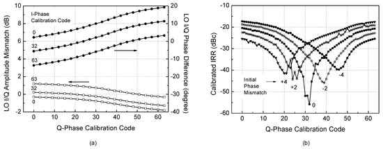
Figure 9.
Simulated I/Q phase mismatch calibration (a). Tuning characteristics of the phase-tunable LO buffer. (b) IRR calibration behavior with respect to the calibration code.
The phase calibration performance for the entire RF transmitter is verified by simulations. To clearly exhibit the calibration effect, initial phase mismatch of −4–+4 degrees is assumed, and the IRR against the calibration code is observed. As can be seen, the calibrated IRR of better than −40 dBc is achieved only with the Q-phase calibration code. Note that this calibrated IRR is not the best achievable because the amplitude mismatch calibration can be further done.
3. Implementation Results
The designed 28-GHz RF transmitter integrated circuit of Figure 1 is fabricated in a 65 nm RF CMOS process. A micrograph of the fabricated chip is shown in Figure 10a. The die size is 1.45 × 1.32 mm2 including the pad frame. The fabricated chip is tested through on-wafer probing. As shown in the measurement setup of Figure 10b, the I/Q baseband and LO signals are supplied by the G-S-S-G probe at the left and G-S-G probe at the bottom, respectively, the RF output signal is probed by G-S-G probe at the right, and the dc and low-frequency serial-peripheral-interface (SPI) signals are supplied through the 15-pin probe from the top. Although not shown here, we also have performed the test by mounting the chip on a printed circuit board (PCB), for which the 15 top-side pins are wire-bonded and the rest key signals of RF, LO, and baseband are probed on the wafer. It has been confirmed that the on-PCB measurements produce more stable and reliable results due to more solid and wide ground plane seen by the chip. A supply voltage of 1.2 V is used.
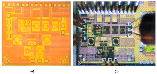
Figure 10.
(a) Chip micrograph. (b) On-wafer probing measurement setup.
Figure 11a is the measured input-to-output power transfer characteristic at 28 GHz. The power gain of the transmitter is +33.3 dB. The output-referred 1 dB compression power OP1dB is +6.5 dBm, and the saturated output power is +12.6 dBm. The simulated and measured results show a good agreement. Figure 11b is the measured frequency response of the power gain. The peak gain is +34 dB at 28.8 GHz, and the 3-dB bandwidth is 27.5–29.3 GHz.
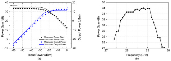
Figure 11.
Measured results. (a) Input-to-output power transfer characteristics. (b) Power gain over the operating frequency.
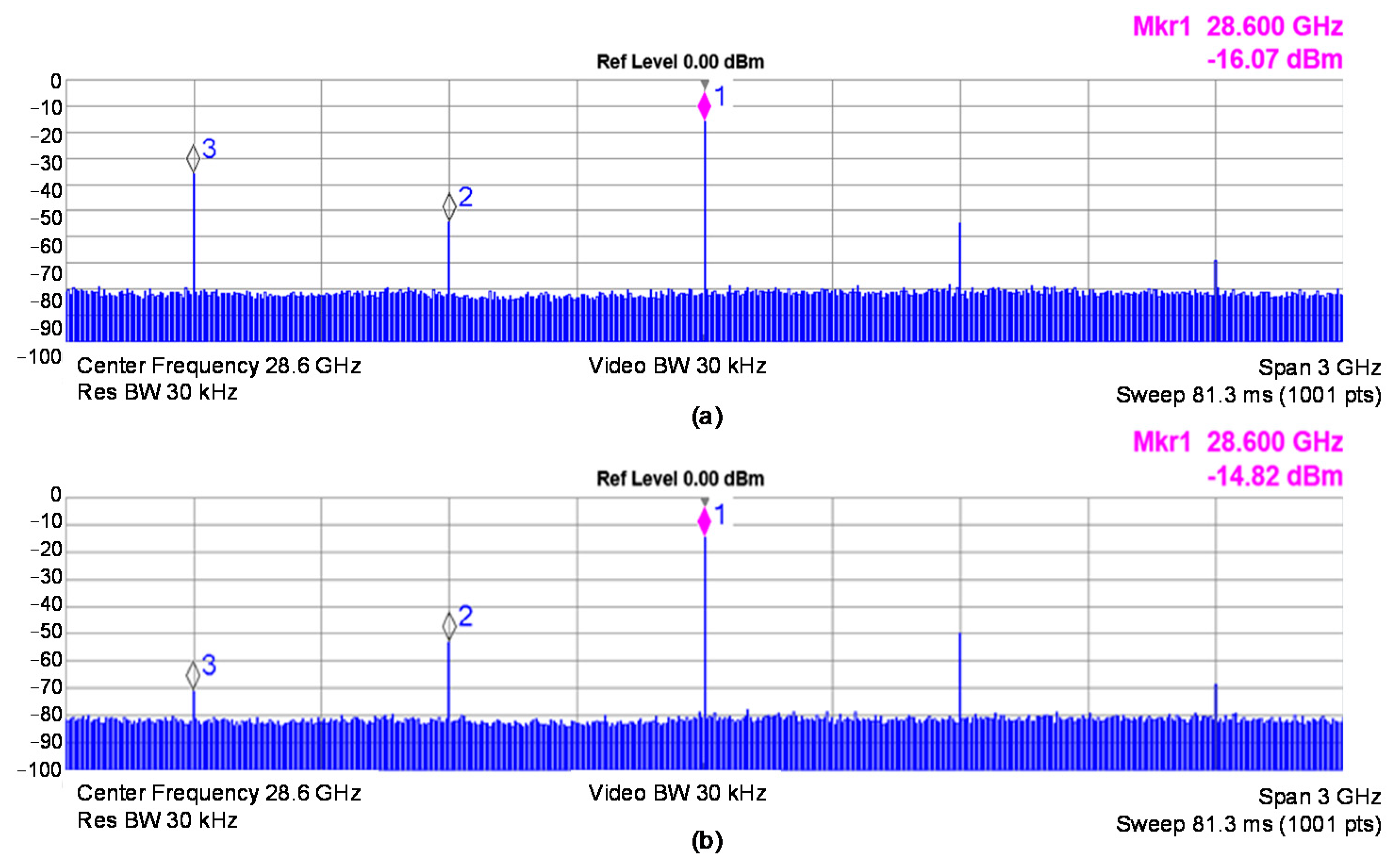
Figure 12 exhibits the measured output spectrum to demonstrate the proposed calibration effect. The baseband and LO frequencies are 600 MHz and 28 GHz, respectively. The output RF frequency appears at 28.6 GHz by the upper-sideband mixing, whereas the LO feedthrough and image components appear at 28 GHz and 27.4 GHz, respectively. It can be seen that the IRR dramatically improves from −19.5 dBc to −55.9 dBc by calibration. The LOFT is found to be −36.8 dBc after the calibration.
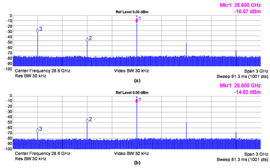
Figure 12.
Measured output spectrum (a) before calibration and (b) after calibration.
The entire calibration process for the RF transmitter includes the dc offset cancellation, I/Q phase mismatch calibration, and finally I/Q amplitude mismatch calibration. However, the dc offset and phase calibration behavior are not shown here for the sake of concise presentation, and only the I/Q amplitude mismatch calibration behavior for the IRR and LOFT is shown in Figure 13. In Figure 13a, we first fix the Q-calibration code at the middle point of 64 and sweep the I-calibration code to find the optimal IRR and LOFT performances. We find the best IRR of −44.9 dBc and LOFT of −39.2 dBc at the I-calibration code of 69. Then, in Figure 13b, we fix the I-calibration code at 69 as found before, and the Q-calibration code is swept. As a result, the best IRR and LOFT are found to be −55.9 dBc and −36.8 dBc, respectively, when the Q-calibration code is 81. Note that the best calibration codes for IRR and LOFT are not identical, so that we need to choose an arbitrary optimal point that makes the IRR and LOFT satisfactory together. In this experiment, it is found to be 69 and 81 for the I- and Q-calibration codes, respectively. The measured calibration results prove that the proposed calibration technique is effective and instrumental for the 28-GHz CMOS direct-conversion RF transmitter.
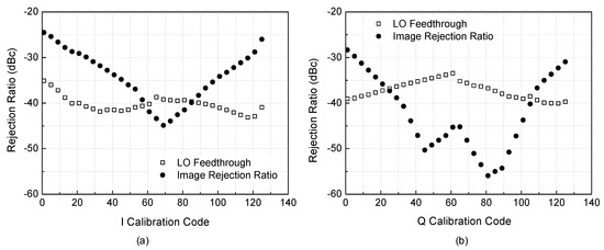
Figure 13.
Calibration performance of IRR and LOFT with respect to (a) Q-calibration code and (b) I-calibration code.
Table 1 summarizes and compares the performances of this work with recent other works. The heterodyne RF transmitters such as the 28 GHz BiCMOS transmitter [8] and 60 GHz CMOS transmitter [10] do not have any I/Q calibration in the mm-wave transmitter because the mm-wave up-conversion is done in a single-phase double-sideband mixing. In contrast, when the mm-wave transmitter is based on the direct conversion architecture, they all presented the I/Q calibrations [2,5,6,7]. One exception is that Lee et al. have demonstrated decent performance without calibration [4], but it is very likely to suffer from severe degradation when process non-uniformity and variation are taken into account in mass production. The previous amplitude mismatch calibration techniques employed in [2,5,6,7] include the digital baseband calibration, RF amplifier gain calibration, and baseband amplifier gain interpolation. Unlike them, our proposed technique is based on the mixer’s gate bias tuning via VDAC, which ensures precise and wide-range I/Q amplitude mismatch calibration. The previous phase mismatch calibration techniques employed in [2,5,6,7] include the QVCO tank capacitor tuning, LO buffer input capacitor tuning, and baseband amplifier phase interpolation. Unlike them, we have proposed to tune the LO buffer’s load capacitance through a varactor with its tuning voltage generated by the VDAC. As a result, we have achieved the IRR of −56.9, which is 12–15 dB better than [5,6,7]. The LOFT of this work is −36.8 dBc which is also comparable to others.

Table 1.
Performance summary and comparison.
4. Conclusions
Improved mismatch calibration techniques are proposed for a 28-GHz millimeter-wave direct-conversion CMOS RF transmitter, which are realized and verified through a 65-nm CMOS integrated circuit. The I/Q amplitude mismatch is calibrated by the gate bias voltage tuning for the switching stage FETs in the up-conversion mixer. The I/Q phase mismatch is calibrated by the varactor capacitor tuning for the LC load in the I/Q LO buffer amplifiers. The dc offset is cancelled by the body bias tuning for the differential pair FETs in the baseband amplifier. It is shown that the proposed mismatch calibration techniques can provide a sufficient calibration precision and cover a wide tuning range. The prototype RF transmitter integrated circuit is realized in 65 nm RF CMOS process and successfully demonstrates satisfactory IRR and LOFT performances through the proposed calibration techniques.
Author Contributions
Conceptualization, Y.L. and H.S.; circuit design and measurements, Y.L. and B.K.; formal analysis, Y.L. and H.S.; investigation, Y.L. and H.S.; data curation and visualization, Y.L. and B.K.; writing, Y.L. and H.S.; supervision H.S.; project administration, H.S.; funding acquisition, H.S. All authors participated for all other aspects. All authors have read and agreed to the published version of the manuscript.
Funding
This research was supported by the National Research Foundation (NRF) of Korea under Grant 2020R1A2C1008484 and Kwangwoon University Research Grant 2021.
Acknowledgments
Computer-aided circuit design tools were supported by the IC Design and Education Center of Korea (IDEC).
Conflicts of Interest
The authors declare no conflict of interest. The funders had no role in the design of the study; in the collection, analyses, or interpretation of data; in the writing of the manuscript, or in the decision to publish the results.
References
- 3rd Generation Partnership Project (3GPP). NR User Equipment (UE) Radio Transmission and Reception; Part 2; Range 2 Standalone; Document 3GPP Technical Specification (TS) Release 15, No. 38.101-2; Valbonne-Sophia Antipolis: Valbonne, France, 2017. [Google Scholar]
- Kim, H.-T.; Park, B.-S.; Song, S.-S.; Moon, T.-S.; Kim, S.-H.; Kim, J.-M.; Chang, J.-Y.; Ho, Y.-C. A 28-GHz CMOS Direct Conversion Transceiver with Packaged 2 × 4 Antenna Array for 5G Cellular System. IEEE J. Solid State Circuits 2018, 53, 1245–1259. [Google Scholar] [CrossRef]
- Power Amplifier Performance Survey 2000-Present. Available online: https://gems.ece.gatech.edu/PA_survey.html (accessed on 25 February 2022).
- Lee, S.; Jeon, Y.; Park, G.; Myung, J.; Lee, S.; Lee, O.; Moon, H.; Nam, I. A 24-GHz RF Transmitter in 65-nm CMOS for In-Cabin Radar Applications. Electronics 2020, 9, 2005. [Google Scholar] [CrossRef]
- Wu, P.-Y.; Gupta, A.K.; Buckwalter, J.F. A Dual-Band Millimeter-Wave Direct-Conversion Transmitter with Quadrature Error Correction. IEEE Trans. Microw. Theory Techn. 2014, 62, 3118–3130. [Google Scholar] [CrossRef]
- Wu, R.; Minami, R.; Tsukui, Y.; Kawai, S.; Seo, Y.; Sato, S.; Kimura, K.; Kondo, S.; Ueno, T.; Fajri, N.; et al. 64-QAM 60-GHz CMOS Transceivers for IEEE 802.11ad/ay. IEEE J. Solid State Circuits 2017, 52, 2871–2891. [Google Scholar] [CrossRef]
- Zhao, D.; Reynaert, P. A 40 nm CMOS E-Band Transmitter with Compact and Symmetric Layout Floor-Plans. IEEE J. Solid State Circuits 2015, 50, 2560–2571. [Google Scholar] [CrossRef]
- Sadhu, B.; Tousi, Y.; Hallin, J.; Sahl, S.; Reynolds, S.; Renstrom, O.; Sjogren, K.; Haapalahti, O.; Mazor, N.; Bokinge, B.; et al. A 28-GHz 32-Element TRX Phased-Array IC with Concurrent Dual-Polarized Operation and Orthogonal Phase and Gain Control for 5G Communications. IEEE J. Solid State Circuits 2017, 52, 3373–3391. [Google Scholar] [CrossRef]
- Cho, Y.; Lee, W.; Park, H.-C.; Park, B.; Lee, J.H.; Kim, J.; Lee, J.; Kim, S.; Park, J.; Park, S.; et al. A 16-Element Phased-Array CMOS Transmitter with Variable Gain Controlled Linear Power Amplifier for 5G New Radio. In Proceedings of the IEEE Radio Frequency Integrated Circuits Symposium (RFIC), Boston, MA, USA, 2–4 June 2019; pp. 247–250. [Google Scholar]
- Saigusa, S.; Mitomo, T.; Okuni, H.; Hosoya, M.; Sai, A.; Kawai, S.; Wang, T.; Furuta, M.; Shiraishi, K.; Ban, K.; et al. A Fully Integrated Single-Chip 60 GHz CMOS Transceiver with Scalable Power Consumption for Proximity Wireless Communication. In Proceedings of the International Solid-State Circuits Conference (ISSCC), San Francisco, CA, USA, 9–13 February 2014; pp. 348–349. [Google Scholar]
- Sadhu, B.; Valdes-Garcia, A.; Plouchart, J.-O.; Ainspan, H.; Gupta, A.K.; Ferriss, M.; Yeck, M.; Sanduleanu, M.; Gu, X.; Baks, C.W.; et al. A 250-mW 60-GHz CMOS Transceiver SoC Integrated with a Four-Element AiP Providing Broad Angular Link Coverage. IEEE J. Solid State Circuits 2020, 55, 1516–1529. [Google Scholar] [CrossRef]
- Kim, B.; Kim, S.; Lee, Y.; Kim, S.; Shin, H. A 28 GHz Quadrature Up-Conversion Transmitter in 65 nm CMOS for 5G mm Wave Radio. In Proceedings of the International System-on-Chip Design Conference (ISOCC), Jeju, Korea, 6–9 October 2019; pp. 31–32. [Google Scholar]
- Lopelli, E.; Spiridon, S.; van der Tang, J. A 40 nm Wideband Direct-Conversion Transmitter with Sub-Sampling-Based Output Power, LO Feedthrough and I/Q Imbalance Calibration. In Proceedings of the International Solid-State Circuits Conference (ISSCC), San Francisco, CA, USA, 20–24 February 2011; pp. 424–425. [Google Scholar]
- Yin, Y.; Chi, B.; Sun, Z.; Zhang, X.; Wang, Z. A 0.1-6.0-GHz Dual-Path SDR Transmitter Supporting Intraband Carrier Aggregation in 65-nm CMOS. IEEE Trans. Large Scale Integr. Syst. 2015, 23, 944–957. [Google Scholar] [CrossRef]
- Kim, J.; Lee, Y.; Chang, S.; Shin, H. Low-Power CMOS Complex Bandpass Filter with Passband Flatness Tunability. Electronics 2020, 9, 494. [Google Scholar] [CrossRef] [Green Version]
- Yen, M.-Y.; Chen, H.-C.; Wei, Y.-L.; Chung, C.-Y. A CMOS Transmitter Analog Baseband for 5G Mobile Communication. Electronics 2019, 8, 1319. [Google Scholar] [CrossRef] [Green Version]
- Kim, J.; Chang, S.; Kim, S.; Shin, H. A 1.2 GHz Bandwidth Baseband Analog Circuit in 65nm CMOS for Millimeter-Wave Radio. In Proceedings of the International System-on-Chip Design Conference (ISOCC), Jeju, Korea, 6–9 October 2019; pp. 301–302. [Google Scholar]
- Sadhu, B.; Bulzacchelli, J.F.; Valdes-Garcia, A. A 28 GHz SiGe BiCMOS Phase Invariant VGA. In Proceedings of the IEEE Radio Frequency Integrated Circuits Symposium (RFIC), San Francisco, CA, USA, 22–24 May 2016; pp. 150–153. [Google Scholar]
- Chang, S.; Shin, H. 2.4-GHz CMOS Bluetooth RF Receiver with Improved IM2 Distortion Tolerance. IEEE Tran. Microw. Theory Tech. 2020, 68, 4589–4598. [Google Scholar] [CrossRef]
- Lee, Y.; Chang, S.; Shin, H. A CMOS RF Receiver with Improved Resilience to OFDM-Induced Second-Order Intermodulation Distortion for MedRadio Biomedical Devices and Sensors. Sensors 2021, 21, 5303. [Google Scholar] [CrossRef] [PubMed]
- Kawai, S.; Minami, R.; Tsukui, Y.; Takeuchi, Y.; Asada, H.; Musa, A.; Murakami, R.; Sato, T.; Bu, Q.; Li, N.; et al. A Digitally-Calibrated 20-Gb/s 60-GHz Direct-Conversion Transceiver in 65-nm CMOS. In Proceedings of the IEEE Radio Frequency Integrated Circuits Symposium (RFIC), Seattle, WA, USA, 2–4 June 2013; pp. 137–140. [Google Scholar]
- Kim, S.; Sohn, J.; Shin, H. A CMOS UHF Harmonic Rejection Transceiver with 2-D LO Phase Calibration for TV White Space Applications. IEEE Trans. Circuits Syst. II Expr. Briefs 2017, 64, 1297–1301. [Google Scholar] [CrossRef]
- Kim, J.; Lee, S.J.; Kim, S.; Ha, J.O.; Eo, Y.S.; Shin, H. A 54–862 MHz CMOS Transceiver for TV-Band White-Space Device Applications. IEEE Trans. Microw. Theory Techn. 2011, 59, 966–977. [Google Scholar] [CrossRef]
- Zhang, W.; He, H.; Wang, R. A 2.0 GHz IQ Imbalance Compensator with Programmable Switch Biases in a Passive Mixer. IEEE Trans. Circuits Syst. II Expr. Briefs 2018, 65, 989–993. [Google Scholar] [CrossRef]
- Chai, Y.; Niu, X.; He, L.; Li, L.; Cui, T.J. A 60-GHz CMOS Broadband Receiver with Digital Calibration, 20-to-75-dB Gain, and 5-dB Noise Figure. IEEE Trans. Microw. Theory Tech. 2017, 65, 3989–4001. [Google Scholar] [CrossRef]
- Liu, Z.; Jiang, Z.; Chen, Z.; Zhang, L.; Liu, H.; Wu, Y.; Zhao, C.; Kang, K. A 24 GHz CMOS Mixer Using Symmetrical Design Methodology with I/Q Imbalance Calibration. In Proceedings of the Asia-Pacific Microwave Conference (APMC), Kuala Lumpur, Malaysia, 13–16 November 2017; pp. 903–905. [Google Scholar]


Publisher’s Note: MDPI stays neutral with regard to jurisdictional claims in published maps and institutional affiliations. |
© 2022 by the authors. Licensee MDPI, Basel, Switzerland. This article is an open access article distributed under the terms and conditions of the Creative Commons Attribution (CC BY) license (https://creativecommons.org/licenses/by/4.0/).