
Low Phase-Noise, 2.4 and 5.8 GHz Dual-Band Frequency Synthesizer with Class-C VCO and Bias-Controlled Charge Pump for RF Wireless Charging System in 180 nm CMOS Process


 ,
, 
Abstract
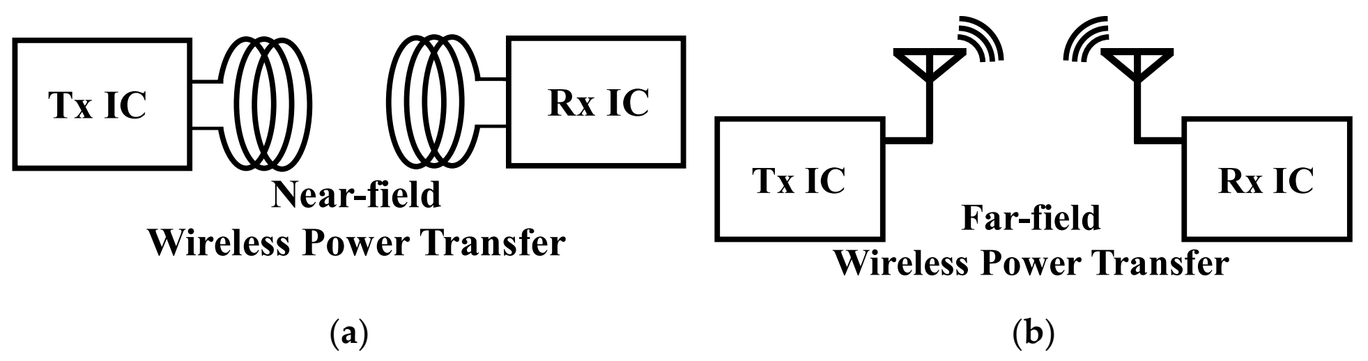
:1. Introduction
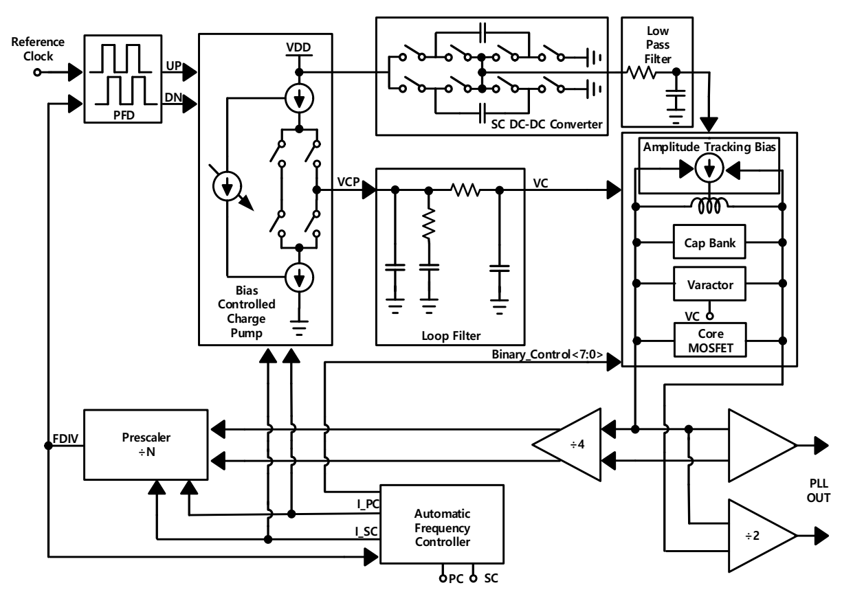
2. Proposed PLL Architecture
3. Building Blocks
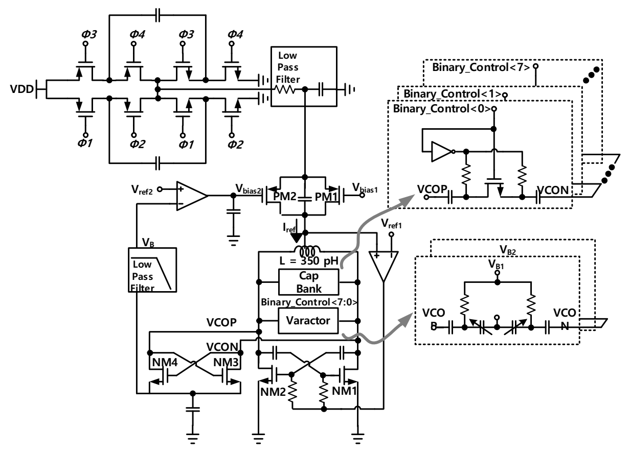
3.1. Constant Amplitude Control Class-C VCO with DC-DC Converter
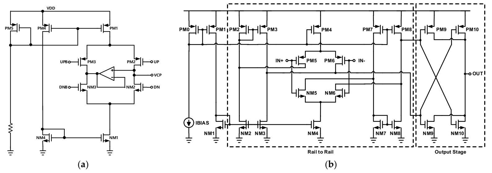
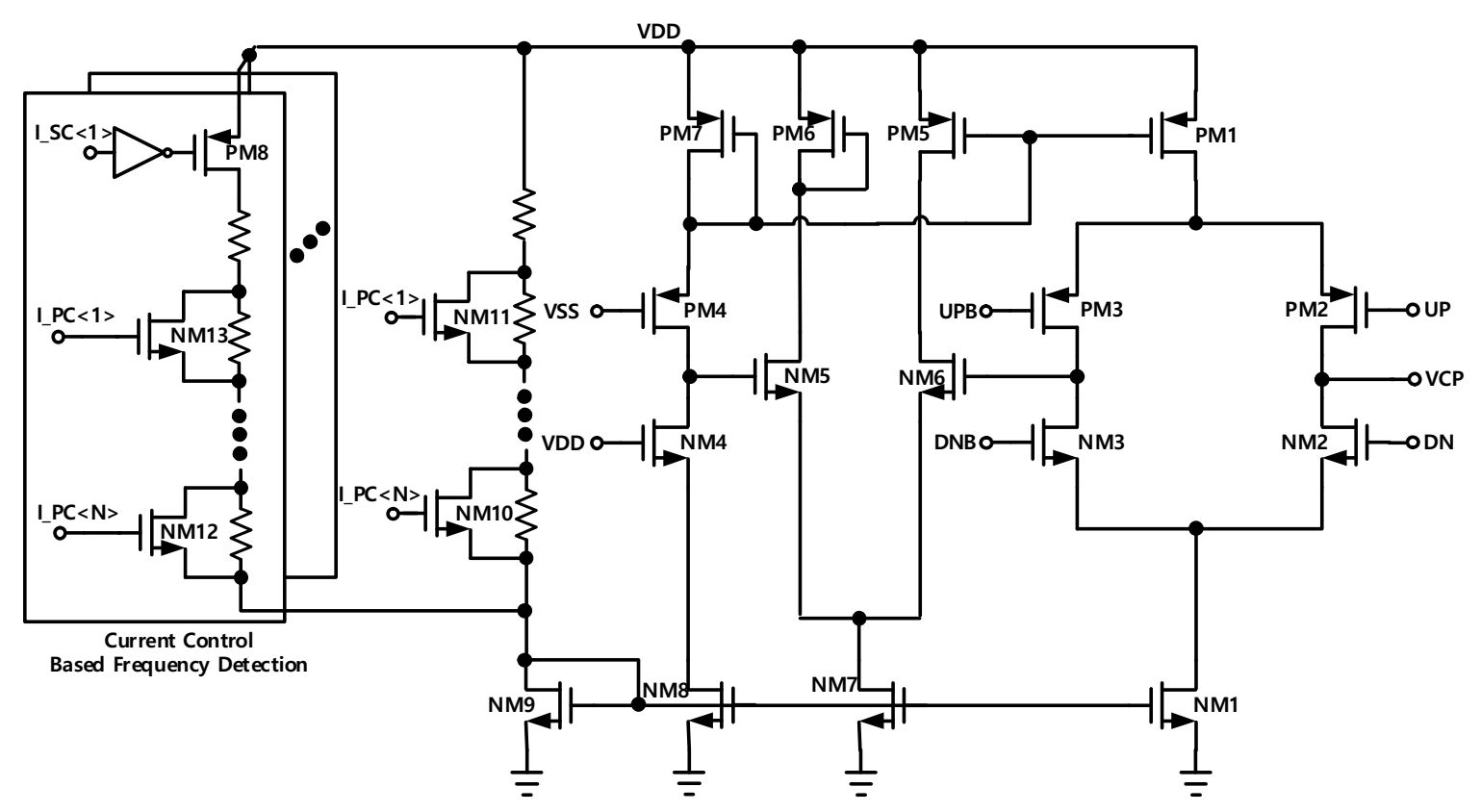
3.2. Bias-Controlled Charge Pump
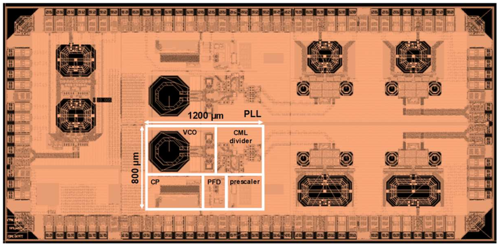
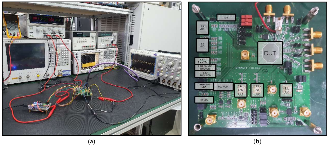
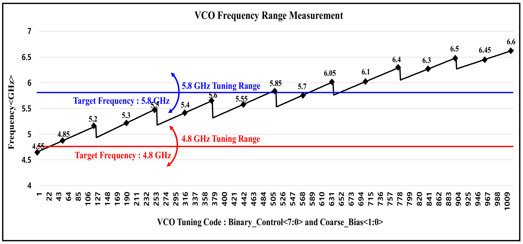
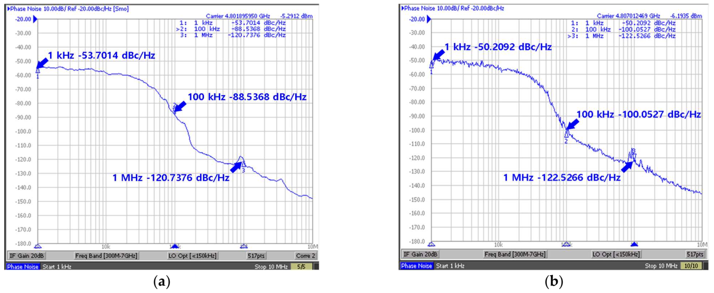
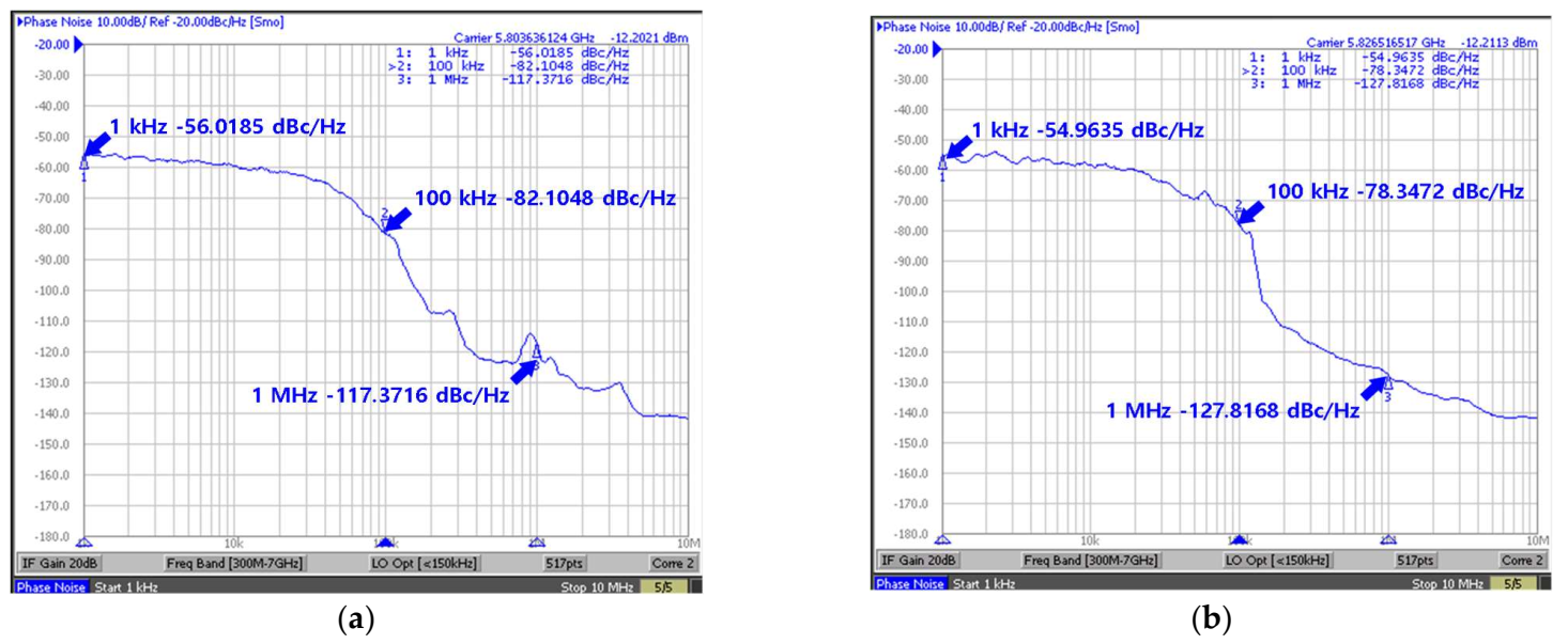
4. Experimental Results
5. Conclusions
Author Contributions
Funding
Acknowledgments
Conflicts of Interest
References
- Xiao, L.; Wang, P.; Niyato, D.; Kim, D.; Han, Z. Wireless networks with RF energy harvesting: A contemporary survey. IEEE Commun. Surv. Tutor. 2015, 17, 757–789. [Google Scholar]
- Lu, Y.; Law, M.-K.; Sin, S.-W.; Seng-Pan, U.; Martins, R.P. A review and design of the on-chip rectifiers for RF energy harvesting. In Proceedings of the IEEE International Wireless Symposium, Shenzhen, China, 30 March–1 April 2015. [Google Scholar]
- Khan, D.; Basim, M.; Shehzad, K.; Ain, Q.; Verma, D.; Asif, M.; Oh, S.J.; Pu, Y.G.; Yoo, S.S.; Hwang, K.C.; et al. A 2.4 Ghz High Efficiency CMOS RF Energy Harvester with Adaptive Path Control. Electronics 2020, 9, 1107. [Google Scholar] [CrossRef]
- Niotaki, K.; Cañavate-Sánchez, M.J.; Collado, A.; Goussetis, G.; Georgiadis, A.; Brazil, T. 2.45/5.8 GHz Dual-Band Power Amplifier for Wireless Power Transfer in Space Applications. In Proceedings of the Active and Passive RF Devices, London, UK, 8 May 2017; pp. 1–4. [Google Scholar]
- Song, C.M.; Lim, H.J.; Son, T.V.; Lee, K.Y.; Yang, Y.G.; Hwang, K.C. Dual-Band RF Wireless Power Transfer System with a Shared-Aperture Dual-Band Tx Array Antenna. Energies 2021, 14, 3803. [Google Scholar] [CrossRef]
- Chen, J.; Jonsson, F.; Carlsson, M.; Hedenas, C.; Zheng, L.-R. A low power, startup ensured and constant amplitude class-C VCO in 0.18 CMOS. IEEE Microw. Wirel. Compon. Lett. 2011, 21, 427–429. [Google Scholar] [CrossRef]
- Zhangming, Z.; Liang, L.; Yintang, Y. A Startup Robust Feedback Class-C VCO with Constant Amplitude Control in 0.18 μm CMOS. IEEE Microw. Wirel. Compon. Lett. 2015, 25, 541–543. [Google Scholar]
- Deng, W.; Okada, K.; Matsuzawa, A. Class-C VCO with amplitude feedback loop for robust start-up and enhanced oscillation swing. IEEE J. Solid-State Circuit 2013, 48, 429–440. [Google Scholar] [CrossRef]
- Shin, J.; Shin, H. A 1.9–3.8 GHz ΔΣ Fractional-N PLL Frequency Synthesizer with Fast Auto-Calibration of Loop Bandwidth and VCO Frequency. IEEE J. Solid-State Circuit 2012, 47, 665–675. [Google Scholar] [CrossRef]
- Roberto, N.; Enzo, P.; Pierpalo, P.; Luca, S. A Design Methodology for MOS Current-Mode Logic Frequency Dividers. IEEE Trans. Circuit Syst. I 2009, 54, 245–254. [Google Scholar]
- Manthena, V.K.; Manh, A.D.; Kiat, S.Y.; Chirn, C.B.; Wei, M.L. Design and Analysis of Ultra Low Power True Single Phase Clock CMOS 2/3 Prescaler. IEEE Trans. Circuit Syst. I 2010, 57, 72–82. [Google Scholar]
- Saravanan, K.; Sankaran, A. Replica bias scheme for efficient power utilization in high-frequency CMOS digital circuits. In Proceedings of the 2014 IEEE International Symposium on Circuits and Systems (ISCAS), Melbourne, Australia, 1–5 June 2014. [Google Scholar]
- Andrea, M.; Pietro, A. A Push-Pull Class-C CMOS VCO. IEEE J. Solid-State Circuit 2013, 48, 724–732. [Google Scholar]
- Hu, A.; Chodavarapu, V.P. Linearization of oscillation frequency for integrated LC-VCO with inversion-mode varactor. Analog. Integr. Circuits Signal Processing 2011, 68, 307–314. [Google Scholar] [CrossRef]
- Hossein, R.K.; Patrick, P.M. A 0.55 mW Fractional-N PLL with a DC-DC Powered Class-D VCO Achieving Better than -66dBc Fractional and Reference Spurs for NB-IoT. In Proceedings of the 2020 IEEE Custom Integrated Circuits Conference (CICC), Boston, MA, USA, 22–25 March 2020; pp. 1–4. [Google Scholar]
- Da Dalt, N.; Sandner, C. A subpicosecond jitter PLL for clock generation in 0.12-μm digital CMOS. IEEE J. Solid State Circuits 2003, 38, 1275–1278. [Google Scholar] [CrossRef]
- Huh, H.; Koo, Y.; Lee, K.Y.; Ok, Y.; Lee, S.; Kwon, D.; Lee, J.; Park, J.; Lee, K.; Jeong, D.-K.; et al. A CMOS dual-band fractional-N synthesizer with reference doubler and compensated charge pump. In Proceedings of the 2004 IEEE International Solid-State Circuits Conference (IEEE Cat. No. 04CH37519), San Francisco, CA, USA, 15–19 February 2004. [Google Scholar]
- Chen, W.Z.; Yu, D.Y. A dual-band four-mode delta sigma frequency synthesizer. In Proceedings of the IEEE Radio Frequency Integrated Circuits (RFIC) Symposium, San Francisco, CA, USA, 10–13 June 2006; pp. 206–207. [Google Scholar]
- Xiaoqiang, L.; Jingwei, Z.; Wenshen, W.; Huimin, L.; Chao, L. A 5.7-6.0 GHz CMOS PLL with low phase noise and -68 dBc reference spur. AEU Int. J. Elec. Communi. 2018, 85, 23–31. [Google Scholar]
- Liu, M.; Ma, R.; Liu, S.; Ding, Z.; Zhang, P.; Zhu, Z. A 5-GHz Low-Power Low-Noise Integer-N Digital Subsampling PLL with SAR ADC PD. IEEE Trans. Microw. Theory Tech. 2018, 66, 4078–4087. [Google Scholar] [CrossRef]
- Liao, D.; Dai, F.F.; Nauta, B.; Klumperink, E.A.M. A 2.4-GHz 16-phase sub-sampling fractional-N PLL with robust soft loop switching. IEEE J. Solid-State Circuits 2018, 53, 715–727. [Google Scholar] [CrossRef]
- Choi, Y.-H.; Kim, B.; Sim, J.-Y.; Park, H.-J. A phase-interpolatorbased fractional counter for all-digital fractional-N phase-locked loop. IEEE Trans. Circuits Syst. II Exp. Briefs Mar. 2017, 64, 249–253. [Google Scholar]
- Liu, Y.H.; Van Den Heuvel, J.; Kuramochi, T.; Busze, B.; Mateman, P.; Chillara, V.K.; Wang, B.; Staszewski, R.B.; Philips, K. An ultra-low power 1.7–2.7 GHz fractional-N sub-sampling digital frequency synthesizer and modulator for IoT applications in 40 nm CMOS. IEEE Trans. Circuits Syst. I Regul. Pap. 2016, 64, 1094–1105. [Google Scholar] [CrossRef]


| Parameter | [19] | [20] | [21] | [22] | [23] | [23] | This Work |
|---|---|---|---|---|---|---|---|
| Technology | 130 nm CMOS | 65 nm CMOS | 65 nm CMOS | 130 nm CMOS | 40 nm CMOS | 40 nm CMOS | 180 nm CMOS |
| Supply Voltage (V) | 1.5 | 1.2 | 1.2 | 1.3 | 1 | 1/0.8 | 1.8 |
| Power Consumption (mW) | 12 | 3.9 | 15.5 | 21 | 1.19 | 1.7 | 8 |
| Bandwidth (kHz) | 100 | 1000 | 500 | 1500 | 1500 | 200 | 100 |
| Reference frequency (MHz) | 32.768 | 50 | 96 | 50 | 40 | 32 | 50 |
| Frequency range (GHz) | 5.7–6.0 | 5.0 | 6.0 | 2.12–2.4 | 1.7–2.7 | 1.7–2.7 | 4.5–6.1 |
| Phase noise (dBc/Hz) | −109 @1 MHz | −108 @1 MHz | −101 @1 MHz | −112 @1 MHz | −109 @1 MHz | −109 @1 MHz | −116.6/−118.5 @1 MHz |
| * FOM (dB) | −193.4 @5.8 GHz | −177.3 @5.8 GHz | −170.6 @5.8 GHz | −162.8 @2.4 GHz | −172.3 @2.4 GHz | −188.4 @2.4 GHz | −202.8 @5.8 GHz −197 @2.4 GHz |
Publisher’s Note: MDPI stays neutral with regard to jurisdictional claims in published maps and institutional affiliations. |
© 2022 by the authors. Licensee MDPI, Basel, Switzerland. This article is an open access article distributed under the terms and conditions of the Creative Commons Attribution (CC BY) license (https://creativecommons.org/licenses/by/4.0/).
Share and Cite
Jo, J.; Kim, D.; Hejazi, A.; Pu, Y.; Jung, Y.; Huh, H.; Kim, S.; Yoo, J.-M.; Lee, K.-Y. Low Phase-Noise, 2.4 and 5.8 GHz Dual-Band Frequency Synthesizer with Class-C VCO and Bias-Controlled Charge Pump for RF Wireless Charging System in 180 nm CMOS Process. Electronics 2022, 11, 1118. https://doi.org/10.3390/electronics11071118
Jo J, Kim D, Hejazi A, Pu Y, Jung Y, Huh H, Kim S, Yoo J-M, Lee K-Y. Low Phase-Noise, 2.4 and 5.8 GHz Dual-Band Frequency Synthesizer with Class-C VCO and Bias-Controlled Charge Pump for RF Wireless Charging System in 180 nm CMOS Process. Electronics. 2022; 11(7):1118. https://doi.org/10.3390/electronics11071118
Chicago/Turabian StyleJo, Jongwan, David Kim, Arash Hejazi, YoungGun Pu, Yeonjae Jung, Hyungki Huh, Seokkee Kim, Joon-Mo Yoo, and Kang-Yoon Lee. 2022. "Low Phase-Noise, 2.4 and 5.8 GHz Dual-Band Frequency Synthesizer with Class-C VCO and Bias-Controlled Charge Pump for RF Wireless Charging System in 180 nm CMOS Process" Electronics 11, no. 7: 1118. https://doi.org/10.3390/electronics11071118
APA StyleJo, J., Kim, D., Hejazi, A., Pu, Y., Jung, Y., Huh, H., Kim, S., Yoo, J.-M., & Lee, K.-Y. (2022). Low Phase-Noise, 2.4 and 5.8 GHz Dual-Band Frequency Synthesizer with Class-C VCO and Bias-Controlled Charge Pump for RF Wireless Charging System in 180 nm CMOS Process. Electronics, 11(7), 1118. https://doi.org/10.3390/electronics11071118