Abstract
The advance in semiconductors and image processing technologies has significantly improved visual quality, especially on mobile consumer devices. The devices require a low-cost and high-bandwidth interface to support various pixel formats on high-resolution displays; thus, the MIPI Alliance has proposed the industry-standard MIPI DSI (Display Serial Interface). The traditional implementation of DSI Rx has classified an incoming packet into three components, a header, a payload, and a checksum, by aligning the packet with the DSI PHY input width and then converting the payload into pixels. Its two-step approach has resulted in high implementation costs for supporting various pixels. This paper proposes a low-cost unified pixel converter, classifying each component and aligning the input payload into various pixel formats in only one step, thus achieving less area and lower power consumption overhead. Two terms are newly introduced for the proposal: a base and a remainder. The base size is the same as the DSI PHY input, and a remainder is a rest after the bases are aligned. The one-pixel size equals a sum of one or more bases and the remainder. The introduction allows us to implement the converter very straightforwardly due to the exact size of the base and the D-PHY input. Additionally, our approach does not require considering the header separately from the payload since the header size equals the base size. Therefore, the header detection unit is eliminated, thus reducing the complexity further. The proposed design was functionally verified in FPGA and synthesized through the Samsung 65 nm standard cell library. The synthesis result showed that the proposed design reduced by 25.7% in the area and 38.6% in the power consumption from the traditional design.
1. Introduction
The advanced semiconductors and image processing technologies have improved the visual quality of consumer devices significantly [1,2]. In particular, the quality of mobile devices, such as smartphones and AR/VR (Augmented Reality and Virtual Reality) devices, is dramatically advancing every day. Most smartphone companies adopt megapixel cameras and high-resolution displays for generating and producing high-quality images [2]. Similarly, the AR/VR devices have high-resolution displays of 120 fps (Frames Per Second) or higher refresh rates for reducing the discrepancy between what eyes see and what a brain perceives.
The higher visual quality involves more data generated from an image source, such as a camera, processed on computing devices and delivered to display devices quickly, thus requiring high computational throughput and bandwidth. For example, the conventional FHD (1080p, 60 fps, 24-bit RGB) display requires a bandwidth of 3.58 Gbps and a high-resolution UHD display (2160p, 60 fps) requires 14.33 Gbps, which is four times larger than the conventional FHD [3]. More data movement implies more power consumption for the transmission; thus, it is essential to implement a power-efficient interface that supports high bandwidth for a mobile device. The MIPI Alliance has been proposing the industry-standard MIPI DSI (Display Serial Interface) for this purpose since 2006 [4], and it is widely adapted to mobile, automotive and multimedia applications [5]. DSI is a packet-based serial interface, and there have been various studies [6,7,8,9,10] on this interface because of its high usability: adding a scramble function to reduce the EMI effect of the PHY layer [8], integrating the CSI of a similar structure with the DSI to increase the effectiveness of the IP [9], reducing the area by re-purposing the buffer to achieve the low power demands of mobile devices [10], and so on.
The DSI Rx receives the D-PHY [11] signal from the DSI Tx source, decodes the input packet for recognizing its header, payload, and checksum, aligns its payload to pixels, and delivers them to a display. The pixel alignment is needed since the display supports various image standards. The DSI Rx IP generally uses two sequence steps for the alignment, called a baseline design in this paper: recognizing and aligning the input packet into the D-PHY output width and then aligning the payload into pixels. The two-step implementation requires a buffer for storing the intermediate result and a large pixel buffer for supporting various bit-width pixel formats, thus resulting in high complexity.
Therefore, this paper proposes a unified pixel converter to process all of them in only one step, thus achieving less area and a lower power consumption overhead. For the design, we consider a packet consisting of not a structure of a header, a payload, and a checksum, but one or multiple bases and a remainder. The base size is the same as the D-PHY input width, and a remainder is a rest after the bases are aligned. One pixel in the MIPI DSI can be expressed as one or more bases and a remainder, i.e., bytes where n is the number of bases, l is the base size, i.e., four, and the remainder (). Our classification, the pixel-oriented approach, allows us to implement the converter very straightforwardly due to the same size of the base and the D-PHY input. Additionally, our approach does not require considering a packet header separately from a payload since the header size equals the base size. Therefore, we can eliminate the header detection unit, thus reducing the complexity further. The proposed design was verified through the FPGA environment and synthesized through the Samsung 65nm standard cell library. As a result, we could reduce 25.7% in the area and 38.6% in the power consumption from the baseline design. As far as we know, there have been no studies targeting pixel alignment, and this is the first attempt to classify and align payloads based on a base and a remainder.
This paper is organized as follows: Section 2 introduces the MIPI DSI standard and protocol, and Section 3 describes the baseline design. Section 4 proposes our unified pixel converter, and Section 5 deals with the proposed design’s verification environment and performance analysis. Finally, the conclusion is made in Section 6.
2. Background
2.1. MIPI Display Serial Interface
MIPI DSI [4] is a low-power and high-performance interface between a mobile device’s application processor and a display module, established by the MIPI Alliance. The interface has been adopted to mobile-influenced market devices, such as smartphones and tablets [5], and recently to wearable devices, such as AR/VR devices [12].
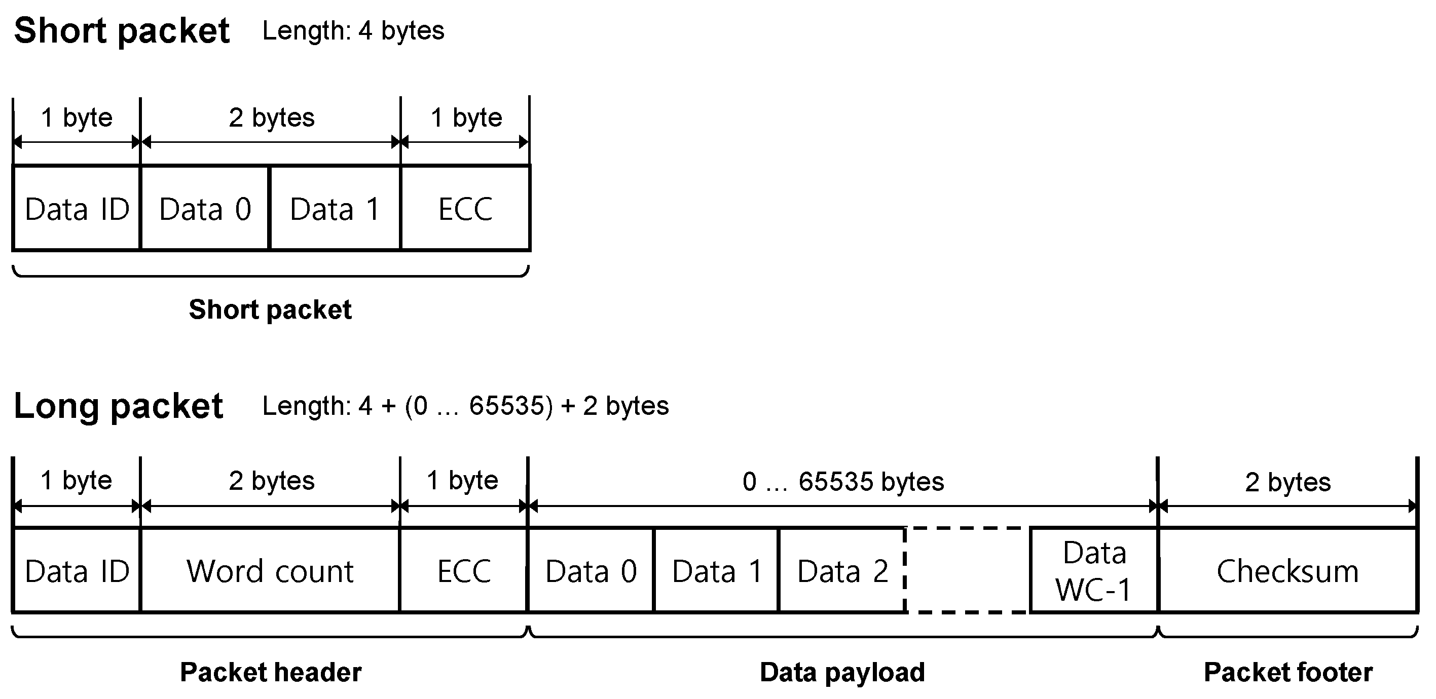
A transaction in the interface consists of one or more packets. There are two types of packets: a 4-byte short packet for the interface configuration and a long packet with a variable length of 6~65,541 bytes for video data transmission, as shown in Figure 1. The short packet consists of a 1-byte data identifier (DI) indicating a packet type, a 2-byte data, and a 1-byte ECC for error correction. The long packet consists of a 4-byte header (a 1-byte DI, a 2-byte word count, a 1-byte ECC, such as the short packet), a 0~65,535-byte data payload, and a 2-byte footer for a checksum for the data payload. The word count indicates the payload size in bytes, where a packet contains video data for a display. A short packet is used for sync timing, such as vsync (vertical sync) and hync (horizontal sync), or an R/W command for internal register control. Meanwhile, a long packet that can load a variable-length payload is used for pixel stream data or vertical/horizontal blanking. To output an image, a sync signal must be periodically transmitted in addition to the image data. For example, after transmitting one frame of one horizontal video line, the hsync signal should be transmitted. In response to these requirements, the host composes and transmits a mixture of a long packet for the pixel stream and a short packet for the hsync.

Figure 1.
A short- and a long-packet structure [4].
2.2. MIPI DSI Standard Pixel Formats
The MIPI DSI standard defines several pixel formats of RGB and YCbCr, and Table 1 shows them with their pixel and byte alignment information.

Table 1.
MIPI DSI standard pixel formats [4].
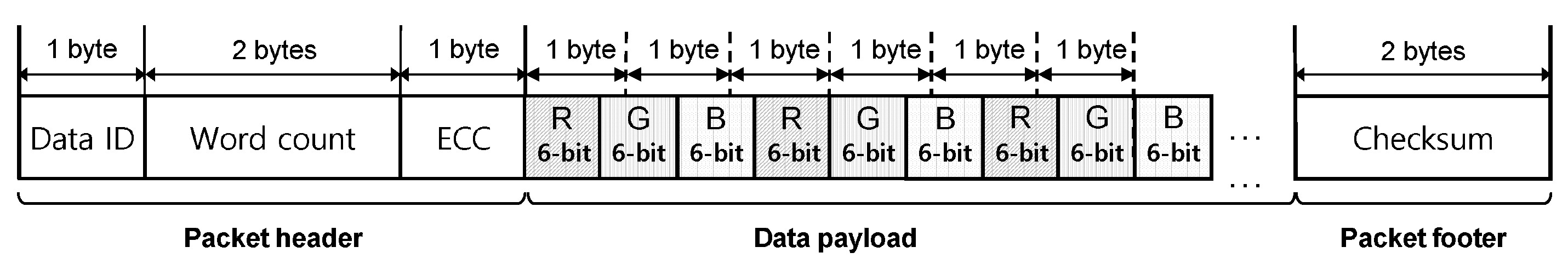
As shown in the table, one pixel is not byte-aligned in some formats, such as 18-bit RGB and 36-bit RGB; thus, in the formats, multiple pixels need to be bundled together (multi-pixel-aligned data) for being delivered to a display module. Figure 2 represents a long-packet transmission for the packed 18-bit RGB pixel format, consisting of groups of R, G, and B 6-bit data for 18-bit pixels. The DSI Rx sends 4 pixels at a time to a display, i.e., 9 bytes (4 pixels × (18 bits/pixel)/(byte/8 bits)). From now on, the multi-pixel-aligned data defined in Table 1 is referred to as a “pixel”.
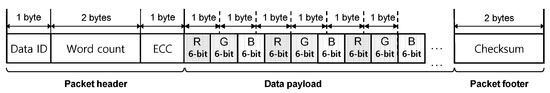
Figure 2.
A packed-pixel stream of the 18-bit RGB format [4].
2.3. Related Work
There is a study related to MPEG2 alignment [13]. In this study, compressed variable-length packets should be processed in 1-byte or 4-byte units. The point of fixing the header parsing position through the alignment is the same as in our study. However, after aligning according to the input lane, the next step (alignment for audio or video data processing or decompression processing) is not covered. Our research proposes a unified pixel converter that can the perform-lane alignment and pixel-format alignment of various sizes at once, significantly reducing overhead compared to the existing structure that requires two steps of alignment or two separate processing units.
Among MIPI IPs, an IP aligns byte data to pixels for the CSI or DSI interface [14]. This IP performs a pixel conversion to RGB666 and RGB888 format in the case of DSI and 8-bit, 10-bit, RAW12, and RGB888 format conversions in the case of CSI, according to the number of lanes. Our research targets all formats defined in the DSI standard, including 30-bit RGB, and implements the DSI IP with a low area overhead through an effective alignment method.
3. A Baseline Design
In the DSI protocol, a host makes one transaction by mixing 4-byte short packets and long packets with a variable length of up to 64 KB, as described in Section 2.1. When a current packet is a long packet with a variable-length payload, the next incoming packet can start at any position of the 4-byte D-PHY input. Therefore, to correctly recognize its header, payload, and checksum, and send the aligned pixels to a display, an incoming packet’s start position should be carefully defined and dynamically changed by the previous packets’ payload sizes.
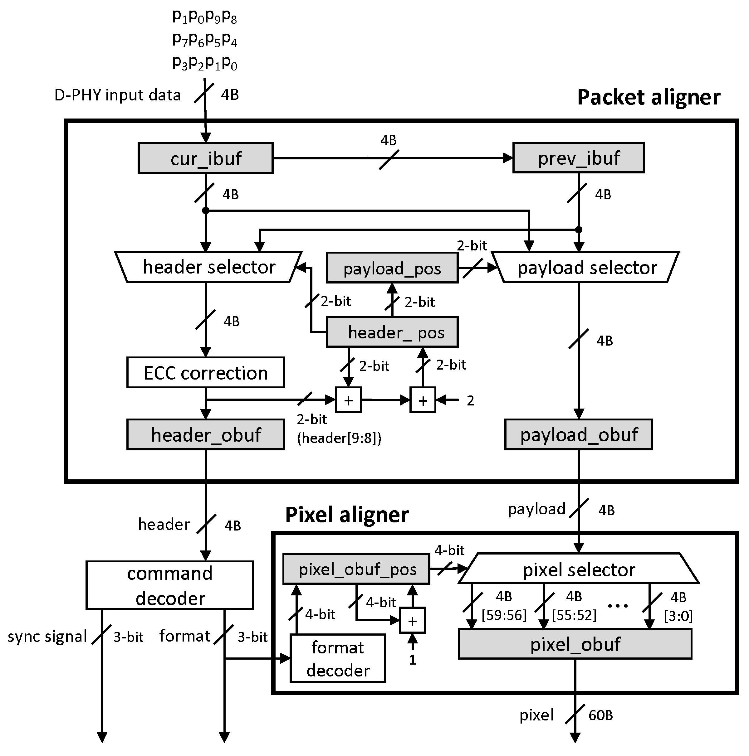
A baseline design for processing the packet alignment is shown in Figure 3, consisting of three components: a packet aligner, a command decoder, and a pixel aligner. The packet aligner aligns the D-PHY inputs in 4-byte units. Then, using the aligned input, the command decoder decodes the header to recognize the pixel format of the payload and provide it to the pixel aligner, rearranging the 4-byte-aligned payload into pixels for the display.

Figure 3.
A baseline design. The gray boxes represent buffers.
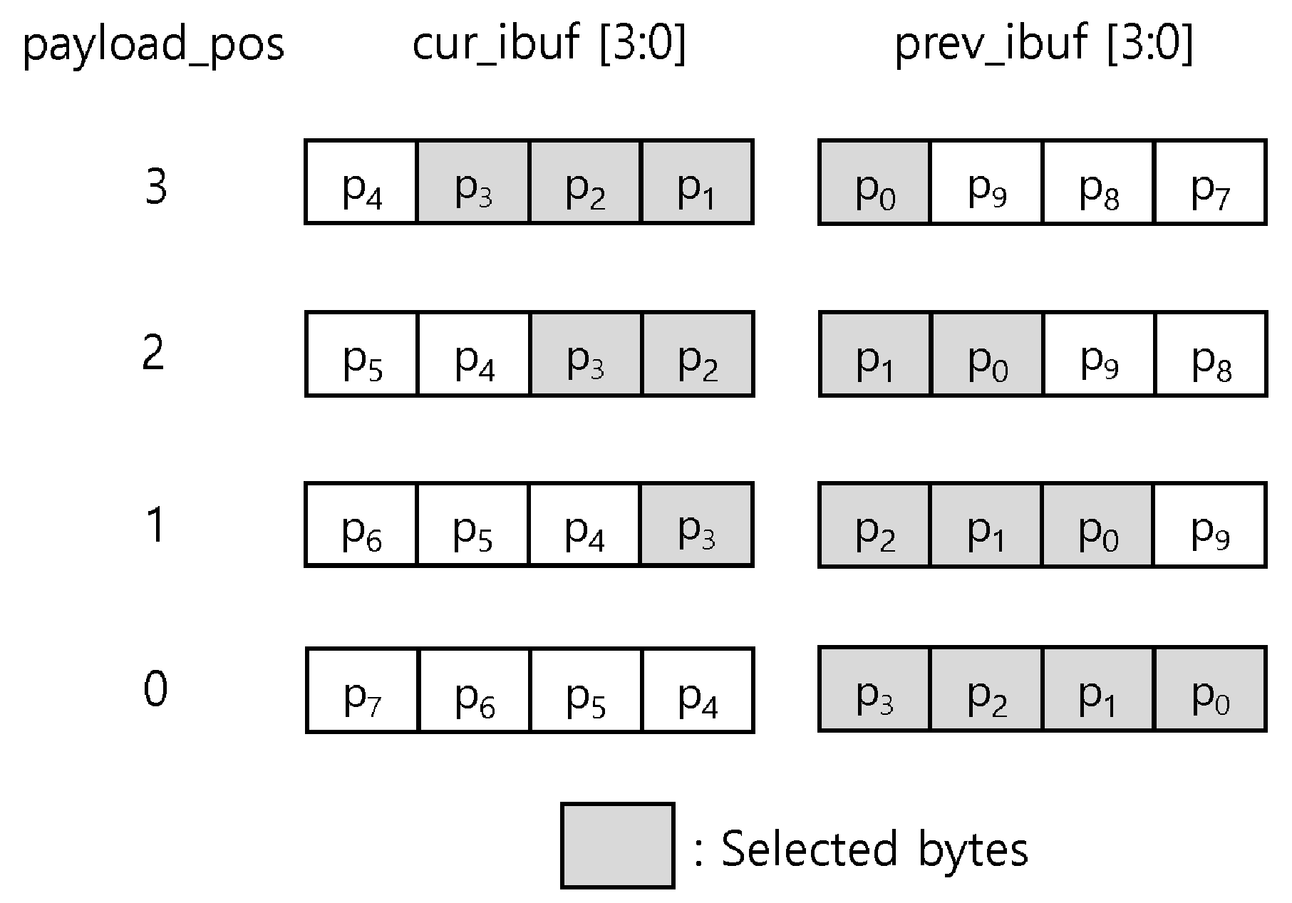
The packet aligner classifies an incoming packet into a 4-byte-aligned header, payload, and checksum. The aligner includes two 4-byte input buffers (cur_ibuf and prev_ibuf), two 4-byte output buffers (header_obuf and payload_obuf), and two select multiplexers (a header selector and a payload selector). At every cycle, new incoming 4-byte data from D-PHY is input to the current input buffer (cur_ibuf), and 4-byte data stored at the current input buffer is moved to the previous input buffer (prev_ibuf) so that the two selectors process the input data of two cycles, i.e., 8 bytes. The header selector selects a 4-byte header from 8 bytes of two input buffers, thus storing the selected header into the header output buffer (header_obuf), optionally enabling the ECC-correction module to perform error detection and correction before storing. The payload selector selects a 4-byte payload from the 8 bytes input from the two input buffers and stores it into the payload output buffer (payload_obuf). Figure 4 shows how the payload selector chooses 4 bytes from the two input buffers, and two buffers are right-shifted by the payload_pos value, the payload selector’s selection value, for the 4-byte alignment.
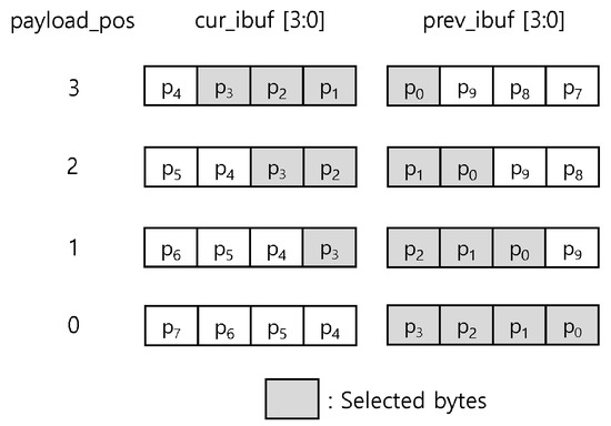
Figure 4.
The behavior of the payload selector in the baseline design according to the payload_pos variable, choosing 4 bytes from two input buffers.
The header selector has the same design as the payload one. The header_pos value, the header selector’s selection value, is initially set to zero when a transaction starts (the transaction starts from lane zero according to the standard), and it changes according to the previous packet sizes. Since one packet length is a sum of the header, the payload, and the checksum, the header position of the next packet from a current packet i can be expressed as the following, where l is the input size in bytes and s(·) represents the size of(·):
Equation (1) can be shortened to Equation (2) since the header size is the same as the D-PHY input size, l, for all packets. Additionally, Equation (2) implies that payload_pos equals header_pos and does not change within the current packet i.
The pixel aligner consists of a demultiplexer (a pixel selector) and a 60-byte pixel output buffer, called pixel_obuf. The pixel selector locates an aligned 4-byte input payload into pixel_obuf depending on the selector’s selection value, pixel_obuf_pos, starting from zero and increasing by one until it reaches the value predefined by each pixel format. For example, if the pixel size is 12 byte, pixel_obuf_pos has values of zero to two. The format decoder provides the maximum value of pixel_obuf_pos, and the input payload is stored from the 4-byt LSB of the output buffer.
Because pixel_obuf has to be aligned to both the pixel sizes (multi-pixel-aligned sizes) shown in Table 1 and the input payload unit (4 byte), we used 60 bytes as the output buffer size, the smallest common multiple, considering the worst-case design. It results from the case of the 15-byte multi-pixel alignment size from the 30-bit RGB format. In this case, the value pixel_obuf_pos repeats from 0 to 14. Therefore, the worst-case design makes the pixel aligner complex, which requires a large output buffer and a pixel selector.
The baseline design has shortcomings: (1) The two independent alignments are required, incurring a significant overhead. (2) The different pixel format requires a different pixel alignment, thus requiring a circuit corresponding to each pixel format. It loses the design flexibility to support multiple pixel formats. In order to support the flexibility, the most oversized pixel alignment design should be considered for the worst case [14].
4. Our Proposal: Unified Pixel Converter
4.1. Overall Design
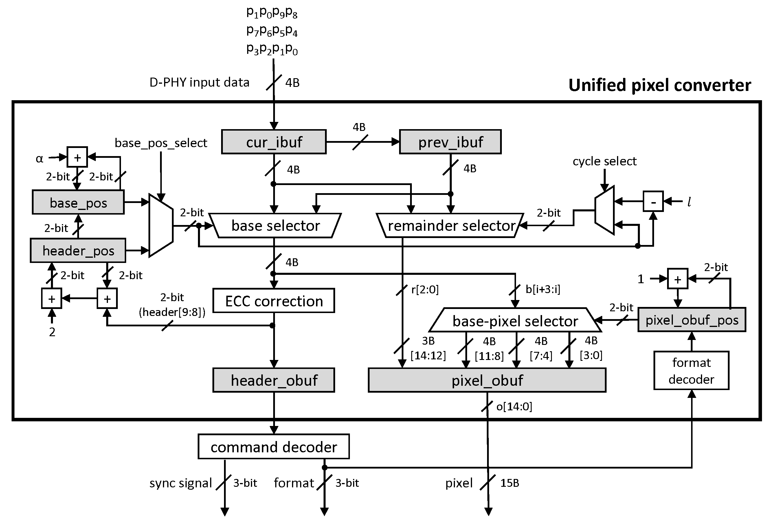
The baseline design classifies one packet into a header, a payload, and a checksum; our unified pixel converter does this into one or more bases and a remainder. The interface input size determines the base size (here, the number of D-PHY lanes, l, i.e., four) and the remainder size (between zero and bytes, i.e., ). This way, we can represent any data size as bytes where , . Therefore, our design can support any size of pixel format. We only need to increase the value of n to support larger pixels. We call as n 4-byte bases and as the remainder. For example, a 15-byte pixel consists of three 4-byte bases and a 3-byte remainder.
Our base and remainder classification allows easy pixel alignment, which is thus sufficient with a much smaller pixel output buffer than the baseline design. Plus, because the header is also 4 bytes, the same size as the base, and the payload follows the header, one base selector can handle both the header and the payload bases. This characteristic eliminates the header alignment logic for the header selection.
Figure 5 shows our unified pixel converter. There are two input buffers, cur_ibuf and prev_ibuf, to store inputs from D-PHY for two cycles, the same as the baseline. Two output buffers, a header output buffer (header_obuf), and a pixel output buffer (pixel_obuf), store a header and a pixel, respectively. The pixel output buffer has a size of 4 to 4n + 3 bytes using a maximum pixel size to be aligned. In this paper, we set the size as 15 bytes, the largest pixel size covered by the standard shown in Table 1, which is much less than 60 bytes in the baseline design. Additionally, there are three selectors: the base selector selects the header and the 4-byte bases () from the two input buffers, the remainder selector selects the remainder (), and the base-pixel selector puts the selected base into the proper position of pixel_obuf.
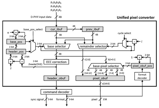
Figure 5.
Our unified pixel converter and a command decoder. The gray box represents for a buffer.
Even when we need to support pixels larger than 15 bytes, our design can benefit from the baseline by not modifying the alignment unit and only supporting an output buffer equal to the size of the largest pixel. Suppose we want to support a pixel set containing multiple prime-number-sized pixels. Our design needs only the largest pixel size buffer regardless of the set’s configuration. On the other hand, the baseline needs the output buffer to be the same size as their least-common multiple, much larger than the maximum-sized pixels, and larger pixel-selector multiplexers.
4.2. Selectors for the Payload and the Pixel Alignments
This section explains how the base, the remainder, and the base-pixel selectors work with their position values.
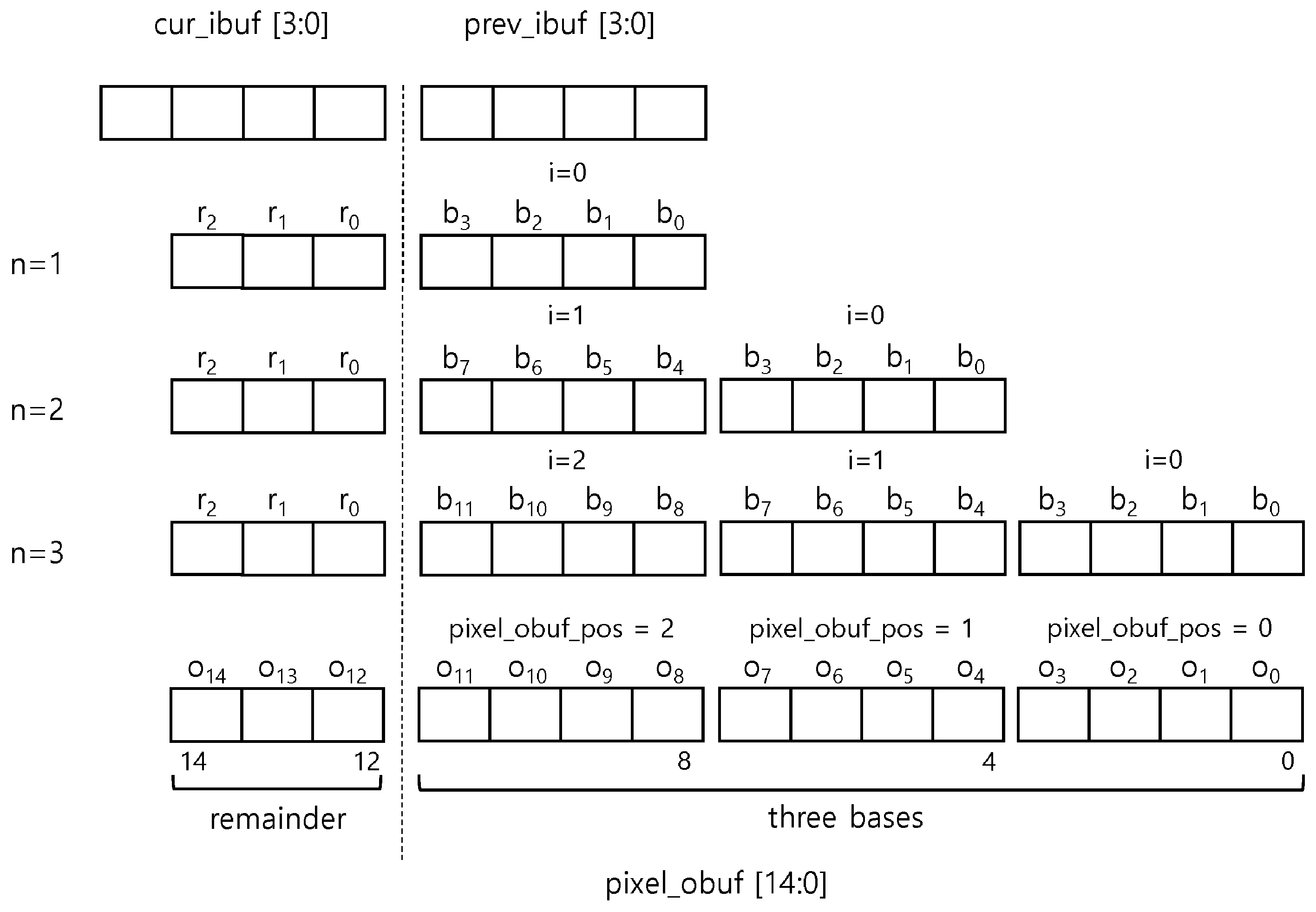
Figure 6 shows the 15-byte pixel output buffer, pixel_obuf, storing the aligned three bases and one remainder. For simplifying our implementation, we align the three MSBs of the output pixel buffer with the cur_ibuf buffer for the remainder and the rest of the output pixel buffer with the prev_ibuf buffer for one and more bases. The base-pixel selector, a demultiplexer, stores the bases to pixel_obuf by the pixel_obuf_pos value. Since the remainder is aligned in cur_ibuf, the remainder goes directly to the most significant 3 bytes of the pixel output buffer, i.e., (pixel_obuf[14:12]), thus not requiring any selector for the remainder. This is our unique approach for optimization, i.e., eliminating the multiplexer for the reminder to the output buffer. Depending on , i.e., the remainder bytes, a display engine can ignore some of the three remainder bytes. The bases are aligned with respect to the remainder location, as shown in the figure. Therefore, the becomes for ith base where . The number three represents the number of bases, which can be stored in the buffer.

Figure 6.
An output pixel buffer, pixel_obuf aligning with the cur_ibuf and the prev_ibuf buffers and showing the base positions depending on n.
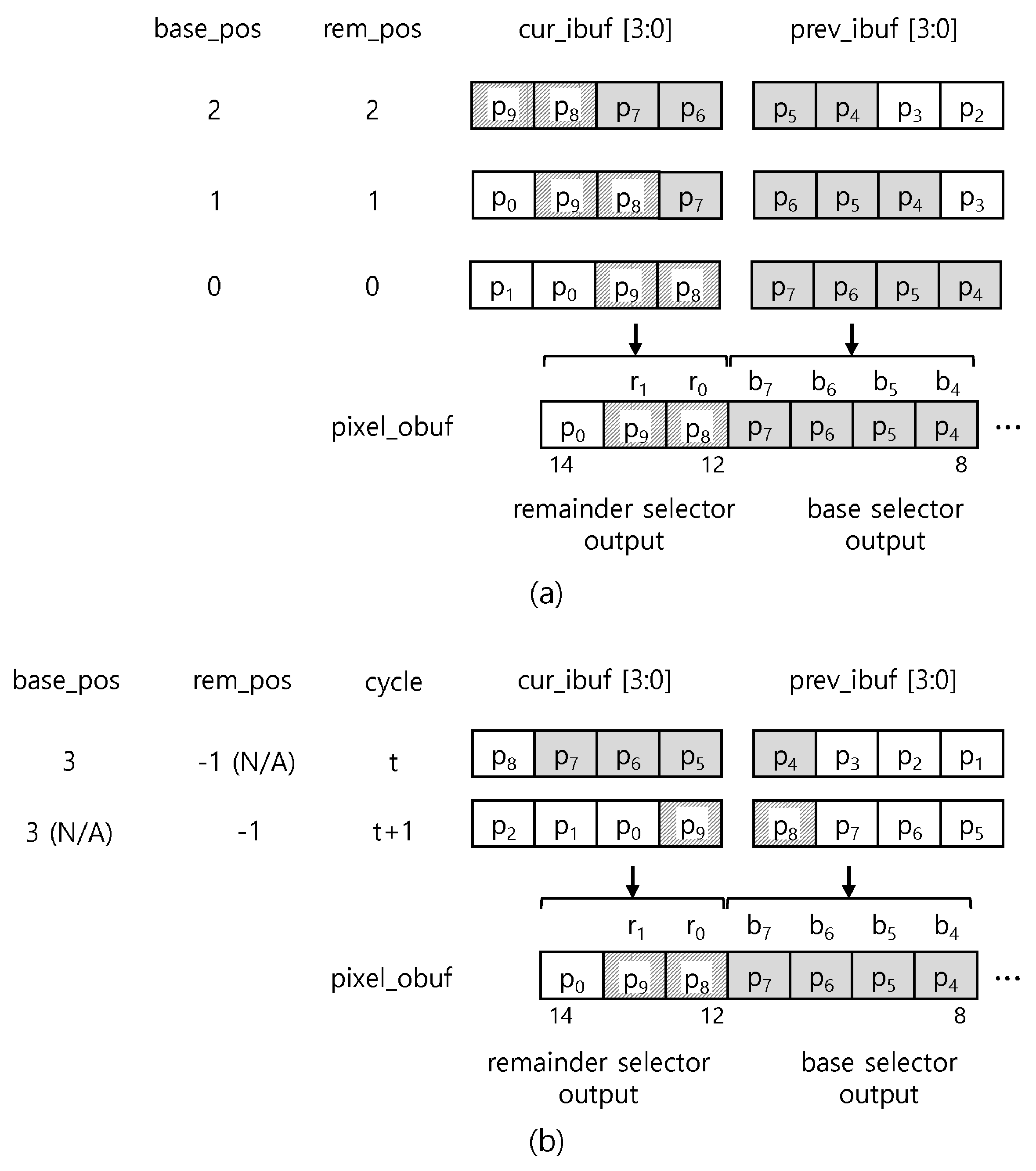
Figure 7a shows how to select the bases and the remainder from two input buffers by base_pos and rem_pos when and . Suppose that we already processed 4 bytes of the first base, . The figure shows a simple case that all the remainder payload bytes are available in cur_ibuf. The base and the remainder selectors right-shift the two input buffer’s data by the same amount of base_pos and rem_pos, producing the aligned 4-byte at the prev_ibuf position and the aligned 2-byte remainder at the cur_ibuf position, respectively. The base and the remainder selectors can be implemented using a barrel shifter.
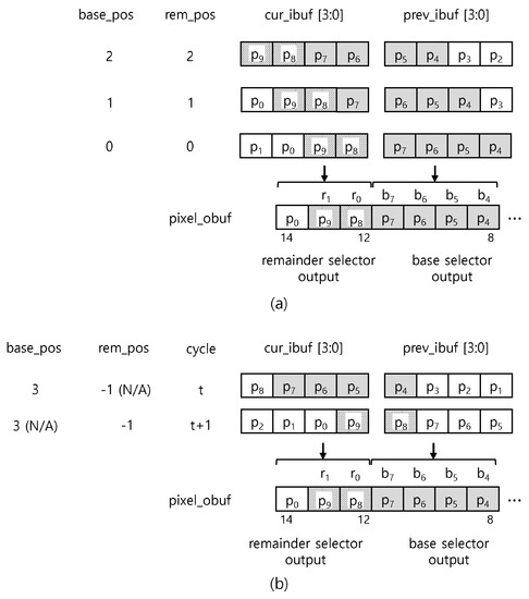
Figure 7.
Example of two input buffer operations when and = 2. The gray bytes represent a current payload. (a) A simple case that all the remainder payload bytes are available in cur_ibuf. (b) A difficult case that all the remainder payload bytes are not available in cur_ibuf.
Figure 7b shows a difficult case in that all the remainder payload bytes are not available in cur_ibuf at cycle t. We select the second base, , at cycle t and the remainder at the next cycle, . At cycle , the LSBs of the remainder are located in prev_ibuf; thus, we need the right-shift by to select the remainder. A negative number means a left-shift. N/A in the position means that the value of the corresponding selector is not used.
4.3. Calculation of Selector Positions
The base position of the ith packet, the jth pixel, and the kth base of a transaction is expressed by the following using Equation (2):
From Equation (3), we know that does not change within a pixel but increases by the remainder, , for the next pixel. base_pos can be implemented simply by using 2-bit adders because only the lower 2 bits of the operation result need to be taken when .
Initially, . Then, from Equations (2) and (3) and for N pixels in a packet,
is obtained from header[9:8] (word count least-significant 2 bit). Therefore, we only need to add 2 and header[9:8] to for the next packet alignment.
We already discussed about controlling the remainder selector in Figure 7. The difficult case implies . Therefore, the selection value for the remainder selector, rem_pos, becomes:
We calculate for every pixel, thus not requiring any additional resource for the calculation.
For ith base, the becomes where . The value of n is a constant, so a counter for is initialized to for the first base.
4.4. Pixel Alignment Example
Figure 8 shows the very first portion of a packet in which 15-byte pixels are continuously transmitting. It represents the operation of each selector and pixel_obuf cycle by cycle when two pixels are transmitted consecutively. Since the pixel size is 15 bytes (n = 3, = 3), we need to select the 4-byte base three times and a 3-byte remainder once to fill the pixel_obuf.
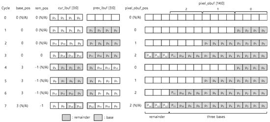
Figure 8.
An example with 9-byte pixel data (n = 3, = 3).
As in Section 2.2, the DSI IP supports various pixel formats, so the output pixel size also varies. Therefore, pixels output from the DSI IP should be aligned to a specific fixed point. For example, sorting on the least significant byte or sorting on the most significant byte can be done depending on the size. In this paper, we implemented fixing the remainder position for the simplicity of the hardware. If necessary, using a base-pixel selector that aligns pixels from the least significant byte is possible with an additional large-size multiplexer for the reminder. The multiplexer stores the remainders of the 6-byte, 9-byte, and 15-byte multi-pixels in Table 1 in [6:5], [8], and [14:12] of the output buffer, respectively.
Initially, base_pos value is set to zero. After that, base_pos is incremented by three for every pixel (because ) by Equation (3). At cycle one, base_pos is zero; accordingly, the selected 4-byte base is grayed out. This selected base fills pixel_obuf according to pixel_obuf_pos. Pixel_obuf_pos increases by 1 from to 2 and is repeated for every pixel. When processing various pixel sizes, fixing the position of the remainder and adjusting the base start position have the advantage, which does not require additional mux for the remainder. The remainder is selected at the same time as the base at cycle three and fills pixel_obuf. rem_pos has the same value of base_pos by Equation (5). The first pixel is the simple case where the remainder fills pixel_obuf with the last base at the same cycle since the remainder is available in cur_ibuf. The second pixel is the difficult case where the remainder fills pixel_obuf at the next cycle after the last base since the remainder is not available in cur_ibuf.
5. Design Verification and Performance Analysis
This section shows the functional verification of the proposed design on FPGA and the synthesis results using the 65 nm standard library for comparing it with the baseline design in terms of area and power consumption.
5.1. FPGA-Based Design Verification and Its Resource Usage
The experiment environment for the FPGA verification is shown in Figure 9a. We configured the environment by connecting the D-PHY signal generator from DGnT [15] and a display to the Xilinx Zynq UltraScale+ MPSoC evaluation platform [16]. We implemented Xilinx D-PHY Rx IP [17], which converts the signal of the D-PHY signal generator into a DSI input, DSI Rx IP, to which the proposed design is applied, and an HDMI output IP to display pixels from the payload on display on the FPGA. The signal generator generated a test pattern of 1080p@60 fps, and the DSI IP operated at 112 MHz. We tested crosshatch, checkboard, and horizontal/vertical RGB patterns. Figure 9b shows the horizontal RGB pattern on the HDMI monitor.
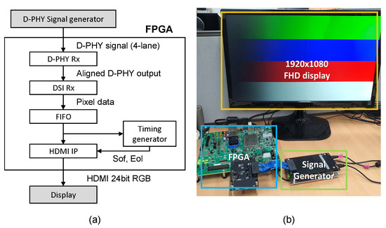
Figure 9.
The verification setup on FPGA. (a) A block diagram. (b) The output on display using a test input from a signal generator.
5.2. Synthesis Result
We performed the synthesis for the area and power analysis using the 65 nm standard library at an operating voltage of 1.08 V and a toggle rate of 10%. The operating frequency was 400 MHz for both designs, which is a sufficient operation speed that can support up to UHD (3840 × 2160)@60 fps. Furthermore, in the case of high-resolution displays, multiple Rx IPs are often used by dividing areas [18], so there is no problem in applying our proposal to commercial products.
Table 2 compares the area of the DSI IP of the baseline with the proposed design. Both used the same LP (low power) Tx and Rx modules for the synthesis, setting configuration registers with the short packet. HS (high speed) Rx represents the baseline design in Figure 3 and our unified pixel converter in Figure 5. The proposed design showed a significant area reduction compared to the baseline: a 34.2% in the HS Rx and a total of 25.7%.
Table 2.
Area comparison (um).
Table 3 compares the major components of each design, explaining Table 2. Both designs can be divided into three main parts: two input buffers, two selectors, and the output alignment logic with multiplexers and buffers. Our design significantly reduced the output alignment from the small output buffer and the small multiplexer for pixel alignment.
Table 3.
Component configuration.
Table 4 shows the results of the overall power consumption, showing that the dynamic power dominated the overall power consumption in both designs, and our design reduced 38.6% from the baseline design. The drastic reduction of the logic size for the pixel alignment results in a significant decrease in the dynamic power.
Table 4.
Power consumption comparison (mW).
6. Conclusions
As the amount of data transferred to display peripherals in a mobile environment increases, the interface’s high bandwidth with a low power consumption becomes essential. The MIPI Alliance has been proposing the industry-standard MIPI DSI for this purpose. The display should support as many pixel formats as possible for the user’s flexibility, but resulting in the implementation overhead for converting the packets into pixels.
In this paper, we proposed a low-cost unified pixel converter to reduce the complexity of the traditional design by classifying packets by a base and a remainder instead of a header and a payload. This concept dramatically reduces the alignment process for the pixel output, making it possible to create DSI IPs with a low hardware overhead while responding to various pixel formats. Our unified pixel-converter design can support various input sizes and output sizes through the base and the remainder concept. Therefore, our approach can be further extended to many other interfaces with a different number of lanes (i.e., 1 to 32 lanes on PCIe [19]) or standards with different data sizes to be aligned (i.e., 188-byte fixed-length packets used by MPEG-2 Transport Stream [20]). The proposed DSI IP was functionally verified in FPGA and synthesized with the Samsung 65 nm process standard library [21] and Synopsys Design Compiler [22], resulting in the reduction of 25.7% in the area and 38.6% in the power consumption.
Author Contributions
K.K. mainly performed the research for this paper; D.K., G.-W.K., S.-Y.K. and S.-W.K. supported his research in different ways. Additionally, S.-W.K. led this project and therefore he is responsible for this research and publication. All authors have read and agreed to the published version of the manuscript.
Funding
This work was supported by ITECH R&D program of MOTIE/KEIT [project No. 20004545, High Luminance 2000PPI MicroLED Backplane and Module Development for AR Devices] and the EDA Tool was supported by the IC Design Education Center (IDEC), Korea.
Conflicts of Interest
The authors declare no conflict of interest.
References
- Cooper, W.; Farrell, S. The Resolution Revolution: How Many Bits Do We Really Need? SMPTE Motion Imaging J. 2017, 126, 1–8. [Google Scholar] [CrossRef]
- Blahnik, V.; Schindelbeck, O. Smartphone imaging technology and its applications. Adv. Opt. Technol. 2021, 10, 145–232. [Google Scholar] [CrossRef]
- Legault, A. Create Higher Resolution Displays with VESA Display Stream Compression. In Proceedings of the MIPI DevCon 2017, Bangalore, India, 27 October 2017; Available online: https://www.mipi.org/sites/default/files/Hsinchu-Hardent-Create-Higher-Resolution-Displays.pdf (accessed on 10 November 2021).
- MIPI Alliance, Inc. Specification for Display Serial Interface (DSI), Version 1.2. 2014. Available online: https://www.mipi.org/node/627 (accessed on 6 March 2022).
- MIPI Display Serial Interface (MIPI DSI). Available online: https://www.mipi.org/specifications/dsi (accessed on 13 September 2021).
- Novatek Microelectronics Corp. MIPI Signal Receiving Apparatus and Method. U.S. Patent 09,077,505, 7 July 2015.
- Samsung Electronics Co., Ltd. System on Chip for Packetizing Multiple Bytes and Data Processing System including the Same. U.S. Patent 10,621,136, 14 April 2020. [Google Scholar]
- Qualcomm Incorporated. Alternating Pseudo-Random Binary Sequence Seeds for MIPI CSI-2 C-PHY. PCT/US2016/050001. U.S. Patent 15/253,020, 27 April 2017.
- Shin, G.-W.; Lee, C.-K.; Lee, Y.-H. Hardware Design of an Interface Supporting Both Camera and Display for Mobile Devices. In Proceedings of the 2015 4th International Conference on Modeling and Simulation (MAS), Jeju Island, Korea, 25–28 November 2015; pp. 17–20. [Google Scholar] [CrossRef]
- Samsung Electronics Co., Ltd. Packet Transmitter and Interface Device including the Same. KR 1,021,950,690,000,, 24 December 2020. [Google Scholar]
- MIPI D-PHY. Available online: https://www.mipi.org/specifications/d-phy (accessed on 2 March 2022).
- Rodriguez, M. High-Performance VR Applications Drive High Resolution Displays with MIPI DSI. In Proceedings of the MIPI DevCon 2018, Seoul, Korea, 19 October 2018; Available online: https://www.mipi.org/sites/default/files/2018-MIPI-DevCon-Rodriguez-Analogix-High-Performance-VR-Apps.pdf (accessed on 1 December 2021).
- Mladenov, T.M.; Mujahid, F.A.; Jung, E.; Har, D. Implementation of High Data Rate Stream Parsing with Data Aligning Mechanism. In Proceedings of the 2006 IEEE International Symposium on Signal Processing and Information Technology, Vancouver, BC, Canada, 27–30 August 2006; pp. 697–701. [Google Scholar] [CrossRef]
- Byte-to-Pixel Converter IP. Available online: https://www.latticesemi.com/-/media/LatticeSemi/Documents/UserManuals/1D2/FPGA-IPUG-02027.ashx?document_id=52142 (accessed on 6 March 2022).
- DGnT Co., Ltd. MIPI Pattern Generator. Available online: http://www.dgnte.com (accessed on 8 March 2022).
- Xilinx. Zynq UltraScale+ MPSoC Data Sheet: Overview (DS891). Available online: https://www.xilinx.com/support/documentation/data_sheets/ds891-zynq-ultrascale-plus-overview.pdf (accessed on 8 March 2022).
- Xilinx. MIPI D-PHY v4.1 LogiCORE IP Product Guide. Available online: https://www.xilinx.com/support/documentation/ip_documentation/mipi_dphy/v4_1/pg202-mipi-dphy.pdf (accessed on 8 March 2022).
- Saar, H. Driving 4K High-Resolution Embedded Displays in New Applications with MIPI DSI and VESA DSC. In Proceedings of the MIPI DevCon 2017, Bangalore, India, 27 October 2017; Available online: https://www.mipi.org/sites/default/files/Bangalore-Synopsys-Driving-4K-Higher-Resolution.pdf (accessed on 1 December 2021).
- Mayhew, D.; Krishnan, V. PCI express and advanced switching: Evolutionary path to building next generation interconnects. In Proceedings of the 2003 11th Symposium on High Performance Interconnects, Stanford, CA, USA, 20–22 August 2003; pp. 21–29. [Google Scholar] [CrossRef]
- Wikipedia. MPEG Transport Stream. Available online: https://en.wikipedia.org/wiki/MPEG_transport_stream (accessed on 6 March 2022).
- Samsung. Samsung 65 nm Process Technology. Available online: https://www.samsungfoundry.com/foundry/homepage/anonymous/technology12inch65nm.do?_mainLayOut=homepageLayout&menuIndex=020105 (accessed on 23 February 2022).
- Synopsys. Design Compiler. Available online: https://www.synopsys.com/implementation-and-signoff/rtl-synthesis-test/dc-ultra.html (accessed on 23 February 2022).


Publisher’s Note: MDPI stays neutral with regard to jurisdictional claims in published maps and institutional affiliations. |
© 2022 by the authors. Licensee MDPI, Basel, Switzerland. This article is an open access article distributed under the terms and conditions of the Creative Commons Attribution (CC BY) license (https://creativecommons.org/licenses/by/4.0/).