Article

A Carbon-Nanotube Cold-Cathode Reflex Klystron Oscillator: Fabrication @ X-Band and Returning Electron Beam Realization

State Key Laboratory of Optoelectronic Materials and Technologies, Guangdong Province Key Laboratory of Display Material and Technology, School of Electronics and Information Technology, Sun Yat-sen University, Guangzhou 510275, China
*
Author to whom correspondence should be addressed.
Electronics 2022, 11(8), 1231; https://doi.org/10.3390/electronics11081231
Submission received: 19 February 2022 / Revised: 1 April 2022 / Accepted: 7 April 2022 / Published: 13 April 2022
(This article belongs to the Section Microelectronics)

Abstract

:
This paper presents the design and fabrication of a reflex klystron oscillator based on a carbon nanotube (CNT) cold-cathode. An X-band klystron oscillator structure is assembled with a CNT cold-cathode electron gun with an electrostatic focusing, a re-entrant cavity as anode, and a repeller. The electron gun adopts a convex CNT film emitter as the cathode. A re-entrant cavity resonating at 8.376 GHz is fabricated. The study mainly focuses on the returning electron beam in the klystron oscillator structure. The experimental results of variations of the anode current and returning electron beam amplitude with repeller voltage are presented. It is demonstrated that a higher extracting voltage of the cold-cathode has an important influence on the returning electron beam. To decelerate electron velocity from the extracting voltage, increasing negative focusing voltage and focusing electrode height in the electron gun can improve the returning electron beam characteristics.

1. Introduction

A reflex klystron oscillator as a microwave source has a short beam tunnel, no use of an external magnet, and a voltage control of the starting current by a repeller [1,2]. It was proposed originally in 1939 [3]. However, the conventional reflex klystron oscillator using a thermionic cathode has significant heat loss, bulky dimensions, and long pre-heating times, which would cause difficulties in several important characteristics, including miniaturization, fast turn-on, and submillimeter-wave band working frequency of the device. A field-emission cold cathode exhibits an instantaneous turn-on response, room temperature operation, and size reduction, which has been applied for novel vacuum devices [4]. Among the field-emission materials, carbon nanotubes (CNTs) have excellent electron-emitting characteristics, such as high current density and electrical conductivity, and high physical stability [4,5,6,7], and have been used as cold cathodes in the study of novel microwave and terahertz frequency sources [8,9,10,11,12,13,14]. The klystron based on a cold-cathode has also been followed with interest by researchers, especially in miniaturization and terahertz band devices [15,16,17,18]. For example, Manohara1 et al. designed a monolithic THz nanoklystron using carbon nanotubes as a cold cathode via photolithography and deep ion etching (DRIE) on a Si substrate and fabricated a CNT cold-cathode [16]. The analytical simulations of terahertz klystron oscillators have been established [17,18,19]. The influence of the incident electron beam aperture angle has also been studied [17]. Although some progress has been made in both the design and analytical simulation, device fabrication and performance remain challenging. For the operation of a reflex klystron oscillator as a closed-loop system, the returning electron beam is crucial to provide a precondition for the electron bunch and to form a feedback mechanism to initiate oscillations. A higher extracting grid-electrode voltage for a reflex klystron oscillator based on a cold-cathode electron gun would affect the returning electron beam characteristics.
In this study, a CNTs cold-cathode e-gun was designed and fabricated. An X-band reflex klystron oscillator prototype structure was designed and assembled based on the CNT gun. A study of the returning electron beam in the device structure was presented. To characterize the effect of high voltage for extracting electrons on the returning electron beam, a threshold voltage was defined, and an approach was proposed to decrease the threshold voltage and improve the characteristics of the returning electron beam. From these results are expected to provide regularities and rules for optimization of start-oscillation conditions for cold-cathode reflex klystron oscillators.

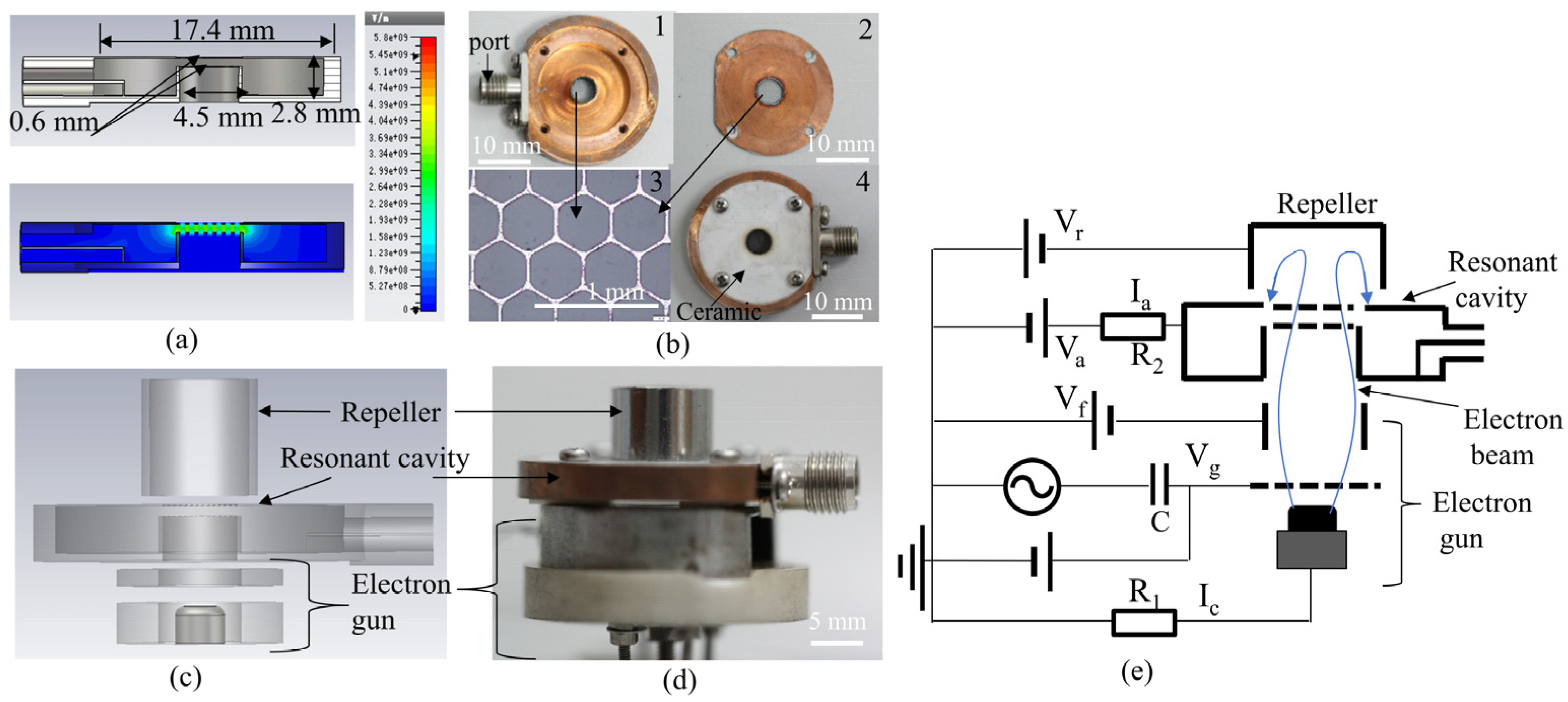
2. Design and Fabrication

A coaxial cold-cathode e-gun was designed and fabricated consisting of a CNT cold cathode, an extracting grid electrode, a ring-shaped focus electrode, and an anode [20], as shown in Figure 1a,b. A ultralong vertical CNT film emitter of about 1.85 mm in height and 3 mm in diameter was prepared by the chemical vapor deposition method [21,22]. The edge morphology of the CNT emitter was shaped as a convex surface with a curvature radius of about 0.5 mm at the edge by a mechanical polishing treatment to eliminate the edge effect [20], as shown in the inset of Figure 1b. The focusing electrode with a ring having an inner diameter of 5 mm and height Hf of 1 mm was placed 1 mm above the grid electrode. Figure 1d shows the electrical scheme of the measurement setup of the electron gun, where the phosphor anode was placed 3 mm above the focus electrode. The cathode voltage was set at 0 V. Direct-current (DC) voltage was applied to the focus electrode and the anode. A pulsed voltage supply was generated using a pulsed power supply combined with a DC power supply. A voltage pulse with a duty cycle of 1.6% at 800 Hz was applied to the grid electrode. A high voltage differential detector (CYBERTEK DP 6150) was connected to the sample resistor R2 in parallel. The voltage waveform was visualized on the oscilloscope (TEKTRONIX MDO 3024). The CNT cold-cathode emission current Ic and anode current Ia could be obtained from the sample resistors R1 and R2 using the relation I = V/R respectively. Figure 1c shows the field emission characteristics of Ic versus grid voltage Vg in the e-gun. A field emission current of 28.3 mA was measured at an electric field of 10 V/μm, and the corresponding emission current density was 400 mA/cm2. The vacuum pressure in the chamber was 5 × 10⁻⁵ Pa. The waveforms of the cathode current Ic, anode current Ia, and grid voltage Vg at a focusing voltage Vf of −50 V were shown in Figure 1e. The spot size of the electron beam on the anode was measured as about 3.8 mm in diameter, as shown in the top half of Figure 1f. The lower half of Figure 1f shows the emission site pattern of the CNT emitter distributed uniformly on an indium tin oxide (ITO) glass anode (captured at a field-emission pulse current of 15 mA) in a diode configuration with a gap of 0.2 mm.
A schematic diagram of the designed re-entrant cavity is shown in Figure 2a. A coupling loop at the sidewall was designed as the output port. The simulation result of the microwave electric field distribution in eigenmode is shown in the bottom part of Figure 2a. Image 4 of Figure 2b shows the photograph of the re-entrant resonant cavity. The lower and upper plate of the cavity are shown in image 1 and 2 of Figure 2b, and the corresponding grids in image 3 of Figure 2b. The resonant frequency of the cavity is 8.376 GHz measured by using a vector network analyzer (KEYSIGHT N5247A). A reflex klystron oscillator structure consisting of the cold-cathode electron gun as an electron-beam source, the re-entrant cavity as an anode, and the repeller was designed and assembled, as shown in Figure 2c,d. The barrel type repeller with an inner-diameter of 6 mm and a height of 7 mm was placed 0.5 mm above the cavity. Figure 2e illustrates the electrical scheme of measurement setup of a reflex klystron oscillator structure.

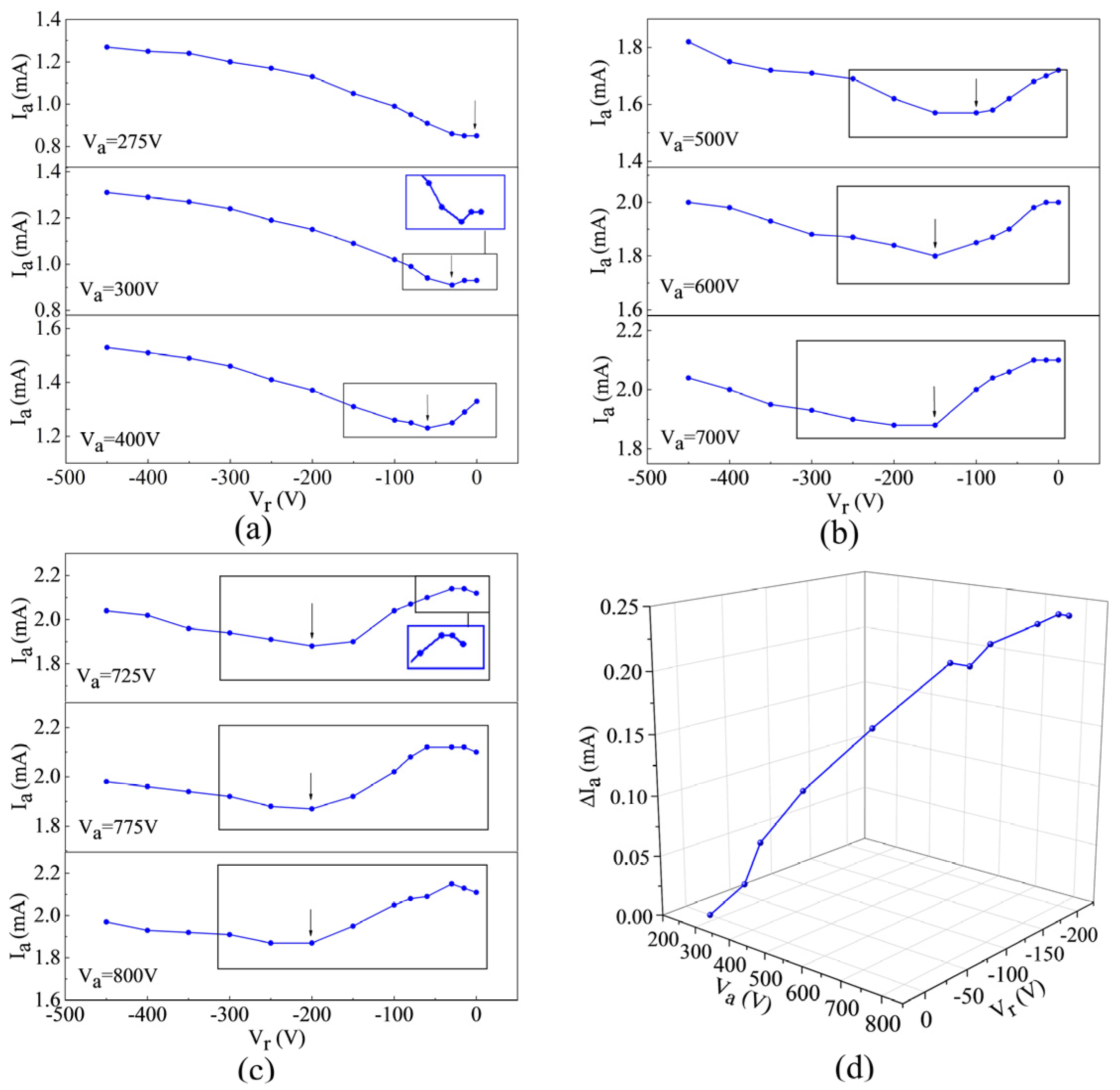
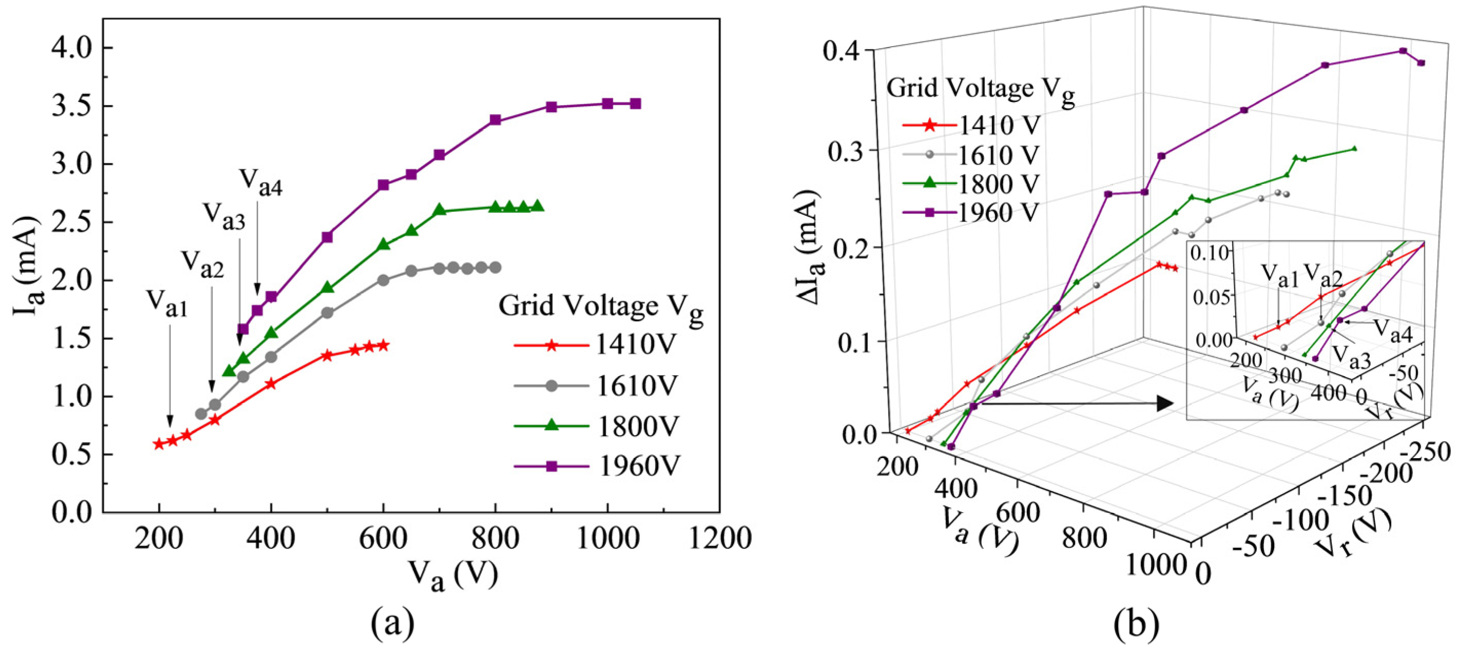
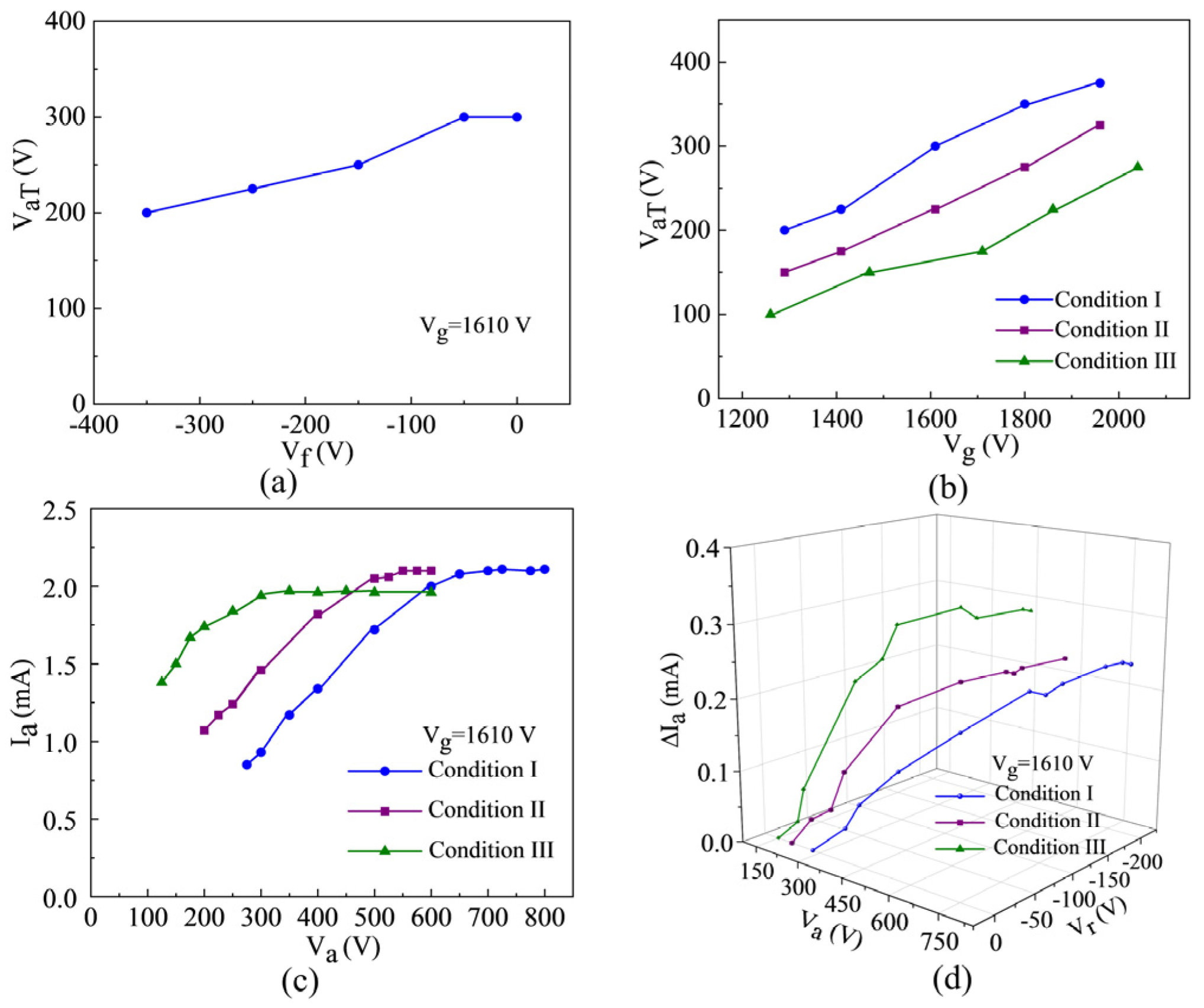
3. Results and Discussion

In the cold-cathode reflex klystron oscillator, the electron beam from the e-gun passes through the gap of the resonant cavity, moves forward to enter the repeller space, and then decelerates and returns to the resonant cavity by the repeller. At a certain anode voltage Va, the anode current Ia originates from the interception of electrons by the grids and walls of the cavity. The negatively biased repeller can repel the electron beam entering the repeller but also can bend the equipotential line and focus the electron beam in the repeller [23]. With the modulation of the repeller voltage Vr, a fraction of the electrons returning to the cavity is not intercepted by the grids of the cavity and forms a returning electron beam. Under the correct feedback conditions [1], the returning electron beam can provide preconditions for the electron bunch to generate an induced current for beam–wave interaction and form a feedback mechanism, which is necessary to initiate oscillations. Because the electron beam returning to the cavity and the forward electron beam occur simultaneously, it is difficult to measure the returning electron beam individually. Here, the returning beam was investigated indirectly by measuring variations of the anode current Ia.
Figure 3a–c show the anode current Ia as a function of the repeller voltage Vr at fixed anode voltages Va. The focusing voltage Vf is fixed at –50 V, and the grid voltage Vg is fixed at 1610 V. Ia increases continuously with Vr ramped up from 0 V to −450 V at Va of 275 V. Ia first decreases and then increases gradually with Vr from 0 V to −450 V at Va between 300 V and 700 V. A valley starts to appear in the curve at Va of 300 V, which is induced by an increase of the returning electron beam, as shown in the black rectangle in Figure 3a–c. Above Va of 700 V, Ia shows the trend of increase, decrease, and increase gradually with Vr from 0 V to −450 V. It is inferred that the electrons that pass through the cavity move forward a short distance and return to the cavity at the anode voltage Va below 275 V. The electric field near the cavity is relatively non-uniform, so most electrons with larger transverse velocity returning to the cavity would be intercepted easily by the cavity with Vr, resulting in an increase in Ia. As Va increases from 300 to 700 V, the electric field near the cavity becomes gradually uniform and facilitates a decrease in the transverse velocity of the electrons. The number of electrons that is not intercepted is gradually more than that intercepted by the grids and walls with low Vr, resulting in a reduction in Ia. However, the repulsive force acting on the electrons increases, and the electric field between the repeller and cavity becomes distorted gradually as the difference between Vr and Va increases; more electrons returning to the cavity are hit easily on the grids and walls of the cavity, which results in an increase in Ia again. The amount of 300 V is thought of as the starting voltage to develop a valley, called threshold voltage VaT. As Va further increases, Ia first increases slightly, as shown in Figure 3c. It is considered that the kinetic energy of electrons through the gap of the cavity at higher Va increases, while the ability of the small Vr to repel and focus the beam returning to the cavity is weak. Thus, a little more electrons fall easily on the cavity. In curves, the valley value (indicated by the black arrow in the black rectangle) gradually shifts to the left and gets larger. Owing to the increasing kinetic energy of electrons with increasing Va, a higher Vr is needed to reflect these electrons along their original path, and the returning electron beam increases. Here, Ia0 is the current at Vr of 0 V, and Iar is the valley value of Ia. In order to numerically illustrate the returning electron beam, ΔIa is calculated by the difference between Ia0 sand Iar to indicate the variation maximum of the returning electron beam amplitude. ΔIa obtained as a function of Va and Vr is shown in Figure 3d. ΔIa increases at first and tends to saturate with Va and Vr.
Figure 4a shows Ia as a function of Va for corresponding to fixed Vg at Vr = 0 V. As Va increases, Ia increases and then tends to saturate. When Vg increases, the cathode emission current Ic increases, and Ia also increases at the same Va. At lower Vg, Ia tends to saturate at lower Va. The voltages of Va1, Va2, Va3, and Va4 are 225 V, 300 V, 350 V, and 375 V, respectively, which are the threshold voltages at corresponding Vg. It is seen that the threshold voltage VaT is higher when Vg is larger. It is deduced that the electrons emitted from the cold-cathode have higher initial velocity, and the electron beam focusing becomes difficult at larger Vg. At the same time, it is more difficult to decelerate the electrons and for them to be well focused axially in the repeller space by Vr, so the number of electrons intercepted increases. Consequently, the larger Vg causes a higher VaT, and a larger threshold voltage is required to improve the electric field near the cavity and the electron beam focusing. Figure 4b shows ΔIa as a function of Va and Vr at fixed Vg. ΔIa corresponding to the above four threshold voltages are shown in the inset of Figure 4b. ΔIa increases and then tends to saturate with Va at fixed Vg. It can be seen that the larger Vg can generate a greater Ia and then a larger ΔIa. The larger ΔIa can generate more electron bunches and a sufficient feedback mechanism.
The large Vg increases the threshold voltage VaT. Therefore, it is expected that decelerating electron velocity entering the repeller space can facilitate lowering of the threshold voltage. Figure 5a shows VaT as a function of Vf. The high negatively biased Vf can decelerate electron velocities from the extracting grid electrode and then decrease VaT. The focusing electrode height Hf can also decelerate electron velocities by extending the time passing through the focusing electrode. Figure 5b shows VaT as a function of Vg at three different conditions, where the condition I is Vf = −50 V and focusing electrode height Hf = 1 mm, the condition II is Vf = −250 V and Hf = 1 mm, and the condition III is Vf = −50 V and Hf = 2 mm. At the same Vg, it has the lowest VaT under the condition III, followed by the condition II. Figure 5c shows Ia as a function of Va, respectively corresponding to the above three conditions at Vg of 1610 V. Figure 5d shows ΔIa as a function of Va and Vr corresponding to above three conditions, respectively, at Vg of 1610 V. Ia and ΔIa under the condition III emerges and saturates at low Va, the condition II at moderate Va, and the condition I at high Va. ΔIa under the condition III is also larger than the other at the same Va. The way to reduce VaT can provide a possibility to decrease the operating voltage. The low operating voltage can reduce the starting current in favor of starting oscillation and power dissipation for a reflex klystron oscillator [8].

4. Conclusions

An X-band reflex klystron oscillator was designed and fabricated based on a cold-cathode electron gun. The cold-cathode electron gun adopted a convex CNT emitter as the cathode. A re-entrant cavity with resonating frequency at 8.376 GHz was fabricated. The relationships between the returning electron beam and the voltages of each electrode in the reflex klystron oscillator structure were studied. The anode current could emerge to decrease with repeller voltage above a threshold voltage, which was induced by an increase of the returning electron beam. The returning electron beam was larger when the anode current was higher. The increase of anode current needed a larger emission current from the cold-cathode by high extracting grid electrode voltage, which caused a high electron emission velocity. It was identified that a high electron emission velocity can increase the threshold voltage and effect the returning electron beam in a reflex klystron oscillator. An approach through increasing negative focusing voltage and height can decelerate electron velocities to reduce the threshold voltage and improve characteristics of the returning electron beam. The study may propose a practical way to reduce the operating voltage in favor of start-oscillation for a cold-cathode reflex klystron oscillator. Moreover, there are several issues that need to be overcome in further studies, including electron beam transmittance, cavity dimensional structure optimization, uncertainty performance on oscillation frequency and stability, etc.

Author Contributions

S.D. conceived the idea and proposed the experimental scheme. S.D. and J.L. initiated the present study. J.L., Y.Z., Y.K. and T.H. carried out the experiments. S.D., J.L. and Y.Z. discussed and interpreted the results. J.L., S.D. and Y.Z. co-wrote the manuscript. All authors have read and agreed to the published version of the manuscript.

Funding

This research was funded by the National Key Research and Development Program of China (Grant no. 2019YFA0210201), the National Natural Science Foundation of China (Grant no. 61874142), the Science and Technology Department of Guangdong Province, and the Fundamental Research Funds for the Central Universities.

Data Availability Statement

The data that support the findings of this study are available from the corresponding author upon reasonable request.

Conflicts of Interest

The authors declare no conflict of interest.

References

  1. Jeon, S.G.; Jin, Y.S.; Kim, J.I.; Kim, G.J.; Shon, C.H. Three-dimensional Particle in-cell Simulations of 300 GHz Reflex Klystrons. J. Appl. Phys. 2007, 101, 054519. [Google Scholar]
  2. Jang, K.H.; Jeon, S.G.; Kim, J.I.; Won, J.H.; So, J.K.; Bak, S.H.; Srivastava, A.; Jung, S.S.; Park, G.S. High Order Mode Oscillation in a Terahertz Photonic-band-gap Multibeam reflex klystron. Appl. Phys. Lett. 2008, 93, 211104. [Google Scholar] [CrossRef]
  3. Varian, R.H.; Varian, S.F. A High Frequency Amplifier and Oscillator. J. Appl. Phys. 1939, 10, 140. [Google Scholar] [CrossRef]
  4. Xu, N.; Huq, S.E. Novel Cold Cathode Materials and Applications. Mat. Sci. Eng. R 2005, 48, 47–189. [Google Scholar] [CrossRef]
  5. Manohara, H.M.; Bronikowski, M.J.; Hoenk, M.; Hunt, B.D.; Siegel, P.H. High-current-density Field Emitters Based on Arrays of Carbon Nanotube Bundles. J. Vac. Sci. Technol. B 2005, 23, 157–161. [Google Scholar]
  6. Iijima, S. Helical microtubules of graphite carbon. Nature 1991, 354, 56–58. [Google Scholar] [CrossRef]
  7. Monthioux, M.; Kuznetsov, V. Who should be given the credit for the discovery of carbon nanotubes? Carbon 2006, 44, 1621–1623. [Google Scholar] [CrossRef]
  8. Teo, K.B.K.; Minoux, E.; Hudanski, L.; Peauger, F.; Schnell, J.-P.; Gangloff, L.; Legagneux, P.; Dieumegard, D.; Amaratunga, G.A.J.; Milne, W.I. Microwave Devices-carbon Nanotubes as Cold Cathodes. Nature 2005, 437, 968–969. [Google Scholar] [CrossRef] [PubMed]
  9. Manohara, H.; Dang, W.L.; Siegel, P.H.; Hoenk, M.; Husain, A.; Scherer, A. Field Emission Testing of Carbon Nanotubes for THz Frequency Vacuum Microtube Sources. In SPIE Reliability, Testing, and Characterization of MEMS/MOEMS III; SPIE: Bellingham, WA, USA, 2003; Volume 5343, pp. 227–234. [Google Scholar]
  10. Xing, Y.; Zhang, Y.; Xu, N.; Huang, H.; Ke, Y.; Li, B.; Chen, J.; She, J.; Deng, S. Design and Realization of Microwave Frequency Multiplier Based on Field Emission from Carbon Nanotubes Cold-Cathode. IEEE Trans. Electron. Dev. 2018, 65, 1146–1150. [Google Scholar] [CrossRef]
  11. Thorpe, J.R.; Fletcher, J.R.; Chamberlain, J.M.; Miles, R.E.; Garcia-Garcia, J.; Mann, C.J.; Huq, E.; Oldfield, M.; Spencer, J. Development of a Submillimeter Wave Reflex Klystrons. In Proceedings of the 10th IEEE International Conference on Terahertz Electronics, Cambridge, UK, 9–10 September 2002. [Google Scholar]
  12. Xing, Y.; Zhang, Y.; Xu, N.; Huang, H.; Ke, Y.; Li, B.; Deng, S. A Cold-Cathode Microwave and Terahertz Radiation Source: Experimental Realization @10′s GHz and Computational Design @THz. IEEE Trans. Electron. Dev. 2019, 40, 1534–1537. [Google Scholar] [CrossRef]
  13. Xu, X.; Yuan, X.; Chen, Q.; Cole, M.T.; Zhang, Y.; Xie, J.; Yin, Y.; Li, H.; Yan, Y. A Low-Voltage, Premodulation Terahertz Oscillator Based on a Carbon Nanotube Cold Cathode. IEEE Trans. Electron. Dev. 2020, 67, 1266–1269. [Google Scholar] [CrossRef]
  14. Yuan, X.; Wang, B.; Cole, M.T.; Zhang, Y.; Deng, S.; Milne, W.I.; Yan, Y. Theoretical Research on a Multibeam Modulated Electron Gun Based on Carbon Nanotube Cold Cathodes. IEEE Trans. Electron. Dev. 2019, 63, 2919–2924. [Google Scholar] [CrossRef] [Green Version]
  15. Jang, K.-H.; Park, S.H.; Lee, K.; Park, G.-S.; Jeong, Y.U. High-order Photonic Bandgap Reflex Klystron Using Carbon Nanotube multi-beam Cathode. Electron. Lett. 2012, 48, 707–708. [Google Scholar] [CrossRef]
  16. Manohara, H.M.; Siegel, P.H.; Marrese, C.; Chang, B.; Xu, J. Design and Fabrication of a Thz Nanoklystron. In Proceedings of the Far-IR, Sub-mm & MM Detector Technology Workshop, Monterey, CA, USA, 1–3 April 2002. [Google Scholar]
  17. Garcia-Garcia, J.; Martín, F.; Miles, R.E. Optimization of Micromachined Reflex Klystrons for Operation at Terahertz Frequencies. IEEE Trans. Microw. Theory Technol. 2004, 52, 2366–2370. [Google Scholar] [CrossRef]
  18. Balucani, M.; Scafè, S.; D’Inzeo, G.; Paffi, A.; Ferrara, V.; Nenzi, P. Nano-Klystron: New Design and Technology for THz Source. In Proceedings of the 6th UK, Europe, China Millimeter Waves and THz Technology Workshop (UCMMT), Rome, Italy, 9–11 September 2013. [Google Scholar]
  19. Jang, K.-H.; Lee, K.; Park, S.H.; Miginsky, S.; Jeong, Y.U. Frequency Multiplying Oscillator with an Electron Beam Accelerated in a Drift Space. Appl. Phys. Lett. 2012, 101, 013507. [Google Scholar] [CrossRef]
  20. Li, J.; Zhang, Y.; Ke, Y.; Li, B.; Deng, S. A Cold Cathode Electron Gun Using Convex Carbon Nanotube Emitter. IEEE Trans. Electron. Dev. 2022, 69, 1457–1460. [Google Scholar] [CrossRef]
  21. Oberlin, A.; Endo, M.; Koyama, T. Filamentous growth of carbon through benzene decomposition. J. Cryst. Growth. 1976, 32, 335–349. [Google Scholar] [CrossRef]
  22. Radushkevich, L.V.; Lukyanovich, V.M. On the structure of carbon produced at thermal decomposition of carbon monoxide on an iron contact. J. Phys. Chem. 1952, 26, 88–95. [Google Scholar]
  23. Fletcher, J.R.; Thorpe, J.R.; Huq, E.; Mann, C.; Steenson, D.P.; Chamberlain, M. Design Considerations for Submillimeter-Wave Reflex Klystrons. IEEE Trans. Microw. Theory Technol. 2004, 52, 2344–2351. [Google Scholar] [CrossRef]
Figure 1. (a) Schematic of electron gun structure. (b) The photograph of the assembled gun. Inset: the CNT cold-cathode. (c) Electron emission characteristics of CNT cold-cathode in the electron gun. Inset: corresponding FN plot. (d) Electrical scheme of measurement setup of a CNT electron gun. (e) Pulsing current and voltage waveforms in the electron gun. (f) Top half: electron beam spot patterns on the phosphor anode. Lower half: emission sites distribution on the ITO anode in a diode configuration.
Electronics 11 01231 g001
Figure 2. (a) The schematic diagram and simulation of the microwave electric field distribution in eigenmode of a re-entrant resonant cavity. (b) Photographs of the re-entrant resonant cavity. Images 1 and 2: lower and top plate of the cavity. Image 3: the close-up of the grid. Image 4: the assembled resonant cavity. (c) Schematic diagram of the reflex klystron oscillator structure. (d) The optical image of the klystron oscillator structure assembled. (e) Electrical scheme of measurement setup of a klystron oscillator structure.
Electronics 11 01231 g002
Figure 3. Ia corresponding to different respective anode voltage Va as a function of the repeller voltage Vr, where (a) Va = 275 V, Va = 300 V (inset: close-up of the variation of Ia), Va = 400 V; (b) Va = 500 V, Va = 600 V, Va = 700 V; (c) Va = 725 V (inset: close-up of the variation of Ia), Va = 775 V, Va = 800 V; (d) ΔIa as a function of Va and Vr.
Electronics 11 01231 g003
Figure 4. Corresponding to fixed Vg at Vr = 0 V: (a) Ia as a function of Va, (b) ΔIa as a function of Va and Vr. Inset of (b): expanded view of the region.
Electronics 11 01231 g004
Figure 5. (a) VaT as a function of Vf. Under three test conditions: (b) VaT as a function of Vg; (c) Ia as a function of Va, where Vg is at 1610 V; (d) ΔIa as a function of Va and Vr, where Vg is at 1610 V.
Electronics 11 01231 g005
Publisher’s Note: MDPI stays neutral with regard to jurisdictional claims in published maps and institutional affiliations.

