Article

A Dual-Mode Control Scheme to Improve Light Load Efficiency for Active-Clamp Flyback Converter

by
Thanh Nhat Trung Tran
1,
Hung-Chia Wang
2 and
Jian-Min Wang
2,*
1
Department of Power Mechanical Engineering, National Formosa University, No. 64, Wunhua Rd., Huwei Township, Yunlin County 632, Taiwan
2
Department of Vehicle Engineering, National Formosa University, No. 64, Wunhua Rd., Huwei Township, Yunlin County 632, Taiwan
*
Author to whom correspondence should be addressed.
Electronics 2022, 11(9), 1308; https://doi.org/10.3390/electronics11091308
Submission received: 8 March 2022 / Revised: 13 April 2022 / Accepted: 19 April 2022 / Published: 20 April 2022
(This article belongs to the Topic Application of Innovative Power Electronic Technologies)

Abstract

:
A novel dual-mode control scheme is proposed in this paper that permits the active-clamp flyback (ACF) converter to operate in both the quasi-resonant (QR) mode under light load and the active-clamp mode under medium or heavy load. The mode transition is performed based on the external dual-mode control circuit. In addition, the proposed converter incorporates a new QR mode valley switching (VS) control circuit that reduces switching loss in the main switch by achieving VS. Under medium to full load, the proposed converter becomes an ACF converter designed to achieve zero-voltage switching (ZVS), which reduces switching losses in both power switches. The proposed dual-mode control ACF converter has the following advantages: (1) compared with conventional ACF converters, the proposed ACF converters minimize switching losses by combining VS and ZVS; (2) under light load conditions, the frequency-limiting QR control mechanism is used to avoid disadvantageous switching losses caused by high switching frequencies. The 65 W ACF converter prototype with a DC 155 V input and a DC 19 V/3.42 A output under 65 kHz switching frequency was implemented. The experimental results demonstrate the feasibility of the proposed control scheme. The efficiency of the proposed converter reached 79% at a load of 3.5 W, which is 11% higher than the conventional ACF converter.

1. Introduction

The flyback converter architecture, as shown in Figure 1, extended from the buck-boost converter, is one of the most popular converters in the power electronics industry. This type of converter is characterized by its simple structure, few components, and easy compliance with electrical isolation safety specifications. Due to the fact of these advantages, flyback architecture is widely used in converters with output power levels less than 100 W such as light-emitting diode (LED) indoor lighting and portable chargers. However, in the transformer of the flyback converter, energy is stored in an air gap in the core. To store enough energy for the transformer, the size of the air gap must be increased with a corresponding increase in the leakage inductance of the transformer, resulting in a voltage spike on the switching device when it is turned off. The snubber circuit is a popular solution for suppressing this voltage spike; however, it lowers converter efficiency.
In recent years, numerous researchers have proposed efficiency improvements for flyback converters. Generally, these improvements can be classified into two major categories: constant-frequency control and variable-frequency control. In constant-frequency control, the active-clamp technique has been widely used in flyback converters. The ACF converter structure and key waveforms are presented in Figure 2a. In this technique, a circuit loop, comprising an auxiliary switch (Q2) and a capacitor (Cclamp), is added at the two terminals on the primary side of the transformer. This loop is used to perform ZVS at the main switch, improving converter efficiency and avoiding the high voltage spikes generated when the main switch is turned off [1,2,3,4,5,6,7]. However, conduction loss caused by resonant circulating current and additional switching in the Q2 switch induces high power loss under light load [8]. Numerous studies [8,9] have described methods for addressing this drawback. Reference [8] employs a secondary-side post-regulator for minimizing power consumption. Consequently, this method requires an external post-regulator, resulting in a circuit with increased cost and size. In [9], a dual-mode control method was adopted in which the operation mode of the ACF converter was divided into two modes based on the load: the conventional flyback mode and the active-clamp mode. Briefly, the proposed converter works as a conventional flyback converter with the auxiliary switch turning off to decrease the converter’s switching and conduction losses under no-load conditions but turns into an ACF converter under normal-load/full-load conditions. However, this method is only effective for reducing the power consumption of the ACF converter under no-load conditions. In categories of variable-frequency control, quasi-resonant (QR) control is the mainstream technique [10,11,12,13,14]. The quasi-resonant flyback (QRF) converter structure and key waveforms are presented in Figure 2b. In the QR control technique, the resonance signal generated by the parasitic capacitance of the switch, COSS, and the magnetizing inductance of the transformer, Lm, are used to turn on the main switch when its drain-source voltage reaches a minimum valley point. Hence, switching loss is significantly reduced. However, this technique cannot achieve ZVS.
Thus, as summarized above, constant-frequency and variable-frequency control have advantages and disadvantages. By combining the advantages of ACF and QRF, a novel dual-mode control scheme combining ZVS and VS is proposed in this paper.
Based on the structure of the ACF converter, in this dual-mode control scheme, an external logic circuit, called a dual-mode switching circuit, is integrated for switching the converter to the QR mode under light load adopting VS for the main switch to substantially reduce switching surges. However, the converter operating in the QR mode may cause high switching frequency and increased switching losses. Thus, the frequency-limiting QR control technology is combined to avoid the disadvantage of the increased switching frequency. This technique limits the maximum switching frequency during light load operation to allow the converter to achieve the frequency-limiting function. Under heavy load, the dual-mode switching circuit switches the converter back to the conventional ACF converter (active-clamp mode) to enable both power switches to achieve ZVS to obtain high efficiency.

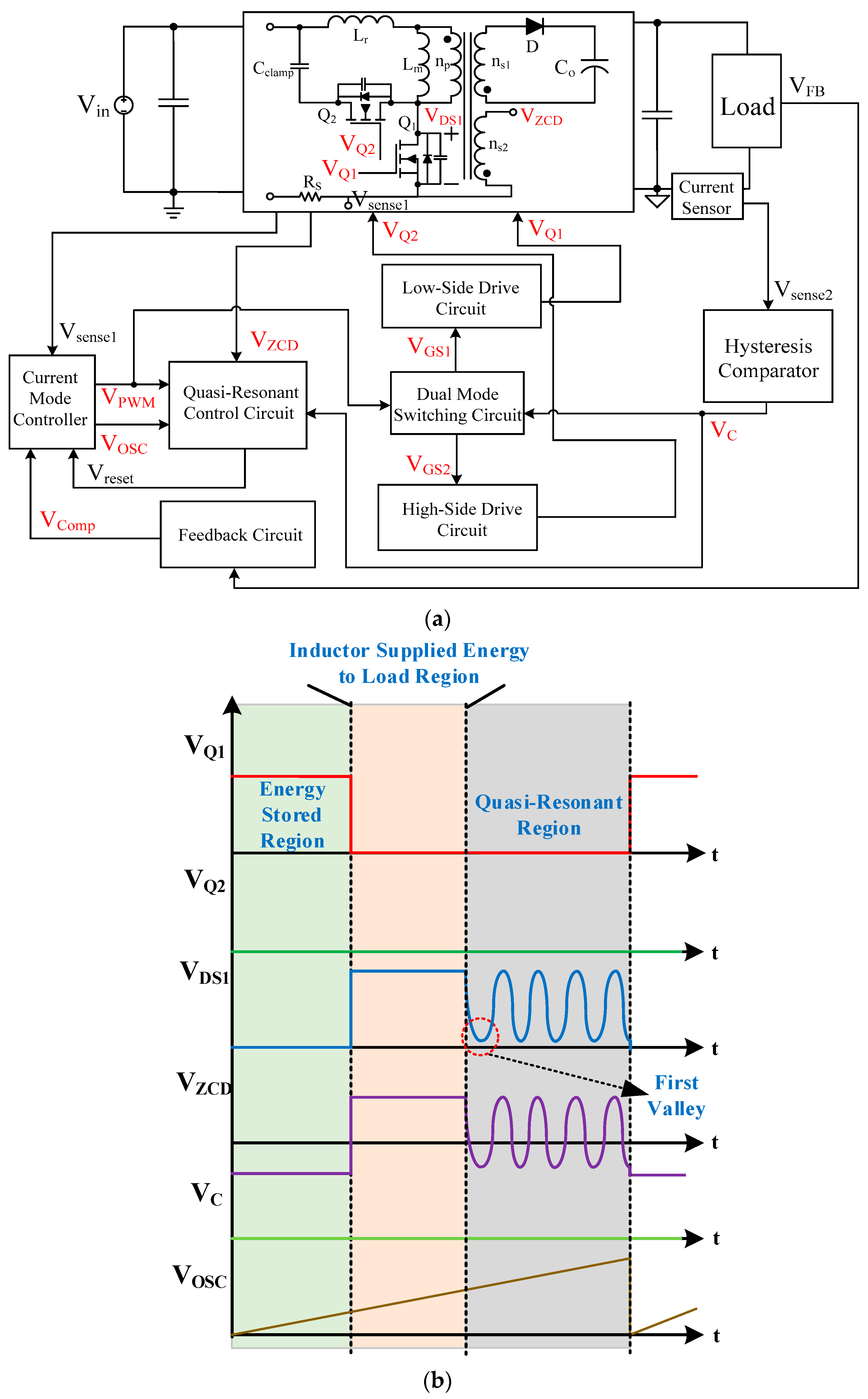
2. Proposed Novel Dual-Mode ACF Converter Structure

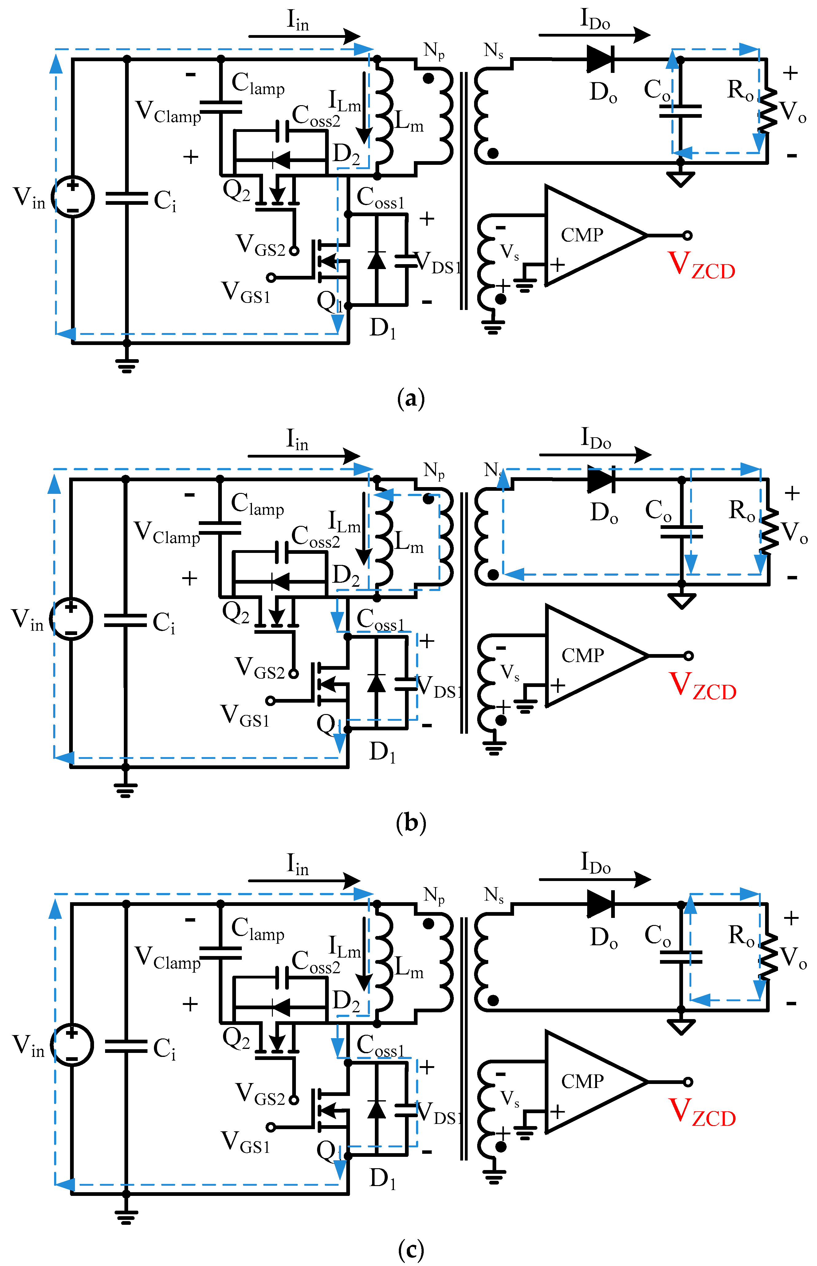
2.1. The Proposed Circuit Structure and Principle of Operation

Figure 3 presents the block diagram of the proposed dual-mode control scheme and the related control sequence diagram under different load conditions. The control circuit consists of the current-mode controller UC3843 produced by STMicroelectronics (Geneva, Switzerland), a QR control circuit, and a dual-mode switching circuit. Among these components, the current mode controller UC3843 plays a critical role in stabilizing the output voltage. The QR control circuit and dual-mode switching circuit are the core circuits of the active-clamp and QR modes, respectively, as shown in Figure 3a. The working principle of the control circuit is explained in terms of two states: light load and heavy load.

2.1.1. Light Load

Under light load, the controller proposed in this paper controls the ACF converter operating in the QR mode, and the related control sequence diagram is illustrated in Figure 3b. In this case, the output signal (VC) of the hysteresis comparator is low; thus, the high-side drive circuit is disabled, turning off the auxiliary switch (Q2) of the converter. At this moment, the feedback voltage signal (VFB) at the converter output is then compared with the internal reference voltage of the feedback circuit to generate the error signal (VComp), which is sent to the current mode controller. The controller processes error signals and generates the control driving signal (VPWM). Notably, the QR mode controller used in this paper has a mechanism to limit the maximum switching frequency, which is different from the conventional first VS method (as indicated by the red dashed circle in Figure 3b); this mechanism avoids disadvantageous switching losses due to the high switching frequencies.

2.1.2. Heavy Load

When the converter transitions from light to heavy load, the operation mode of the converter is switched from the QR mode to the active-clamp mode by the controller. Figure 3c depicts the related control sequence diagram. At this moment, the magnitude of the error signal (VComp) generated by the feedback circuit increases, simultaneously increasing the duty cycle of the drive signal (VPWM) generated by the current mode controller. Due to the hysteresis comparator output signal (VC) in this state being high, the high-side drive circuit is enabled. Consequently, the auxiliary switch of the ACF Q2 is activated in accordance with the drive signal of VQ2. In other words, the driving signals VQ1 and VQ2 are complementary operation signals.

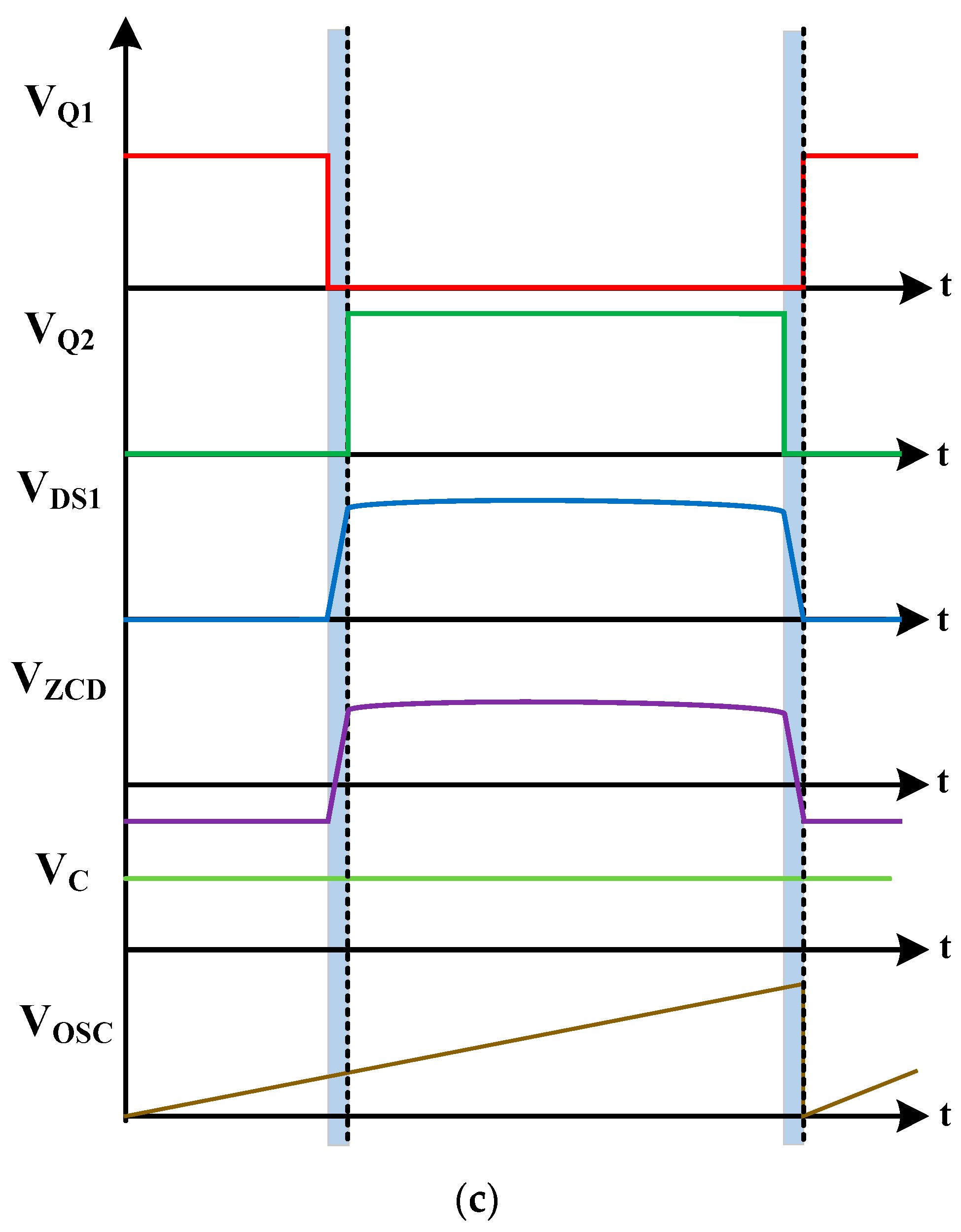
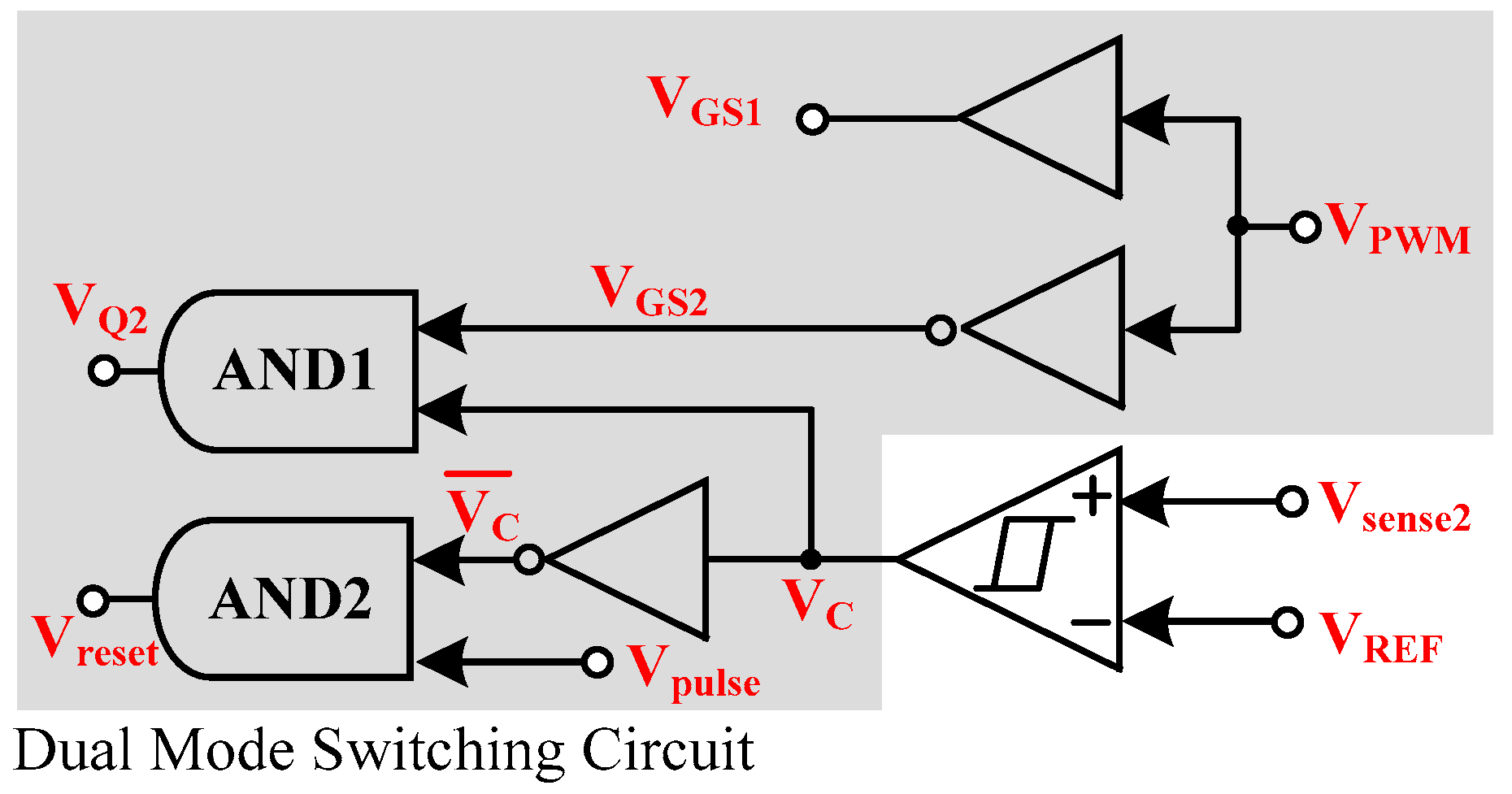
2.2. The Control Circuit of the Proposed Novel Dual-Mode ACF Converter

This section describes the control circuit of the dual-mode ACF proposed in this paper.

2.2.1. Dual-Mode Switching Circuit

The gray block in Figure 4 is a dual-mode switching circuit. When the converter is operating under light load, the hysteresis comparator output (VC) is low, since the output voltage of the current sensor (Vsense2) is less than the reference voltage (VREF). Therefore, the drive signal (VQ2) of the high-side auxiliary switch remains low. The input signal (Vpulse) of the second AND gate (AND2) determines the state of the valley trigger signal (Vreset) because the voltage signal (VC) becomes high after the NOT gate. The valley trigger signal (Vreset) resets the main controller, which can precisely control the low-side main switch (Q1) to achieve VS and to enable the converter to operate in the QR mode.
When the converter is operating under heavy load, the hysteresis comparator output (VC) is high; thus, the output state of the first AND gate (AND1) is determined by the voltage signal, VGS2. At this moment, the high-side auxiliary switch begins to operate. For the second AND gate (AND2), the output voltage signal (Vreset) is low since the signal (VC) is high, and the main controller is not affected by the reset signal. In this stage, the QR control circuit is disabled, enabling the transition of the converter to the active-clamp mode.

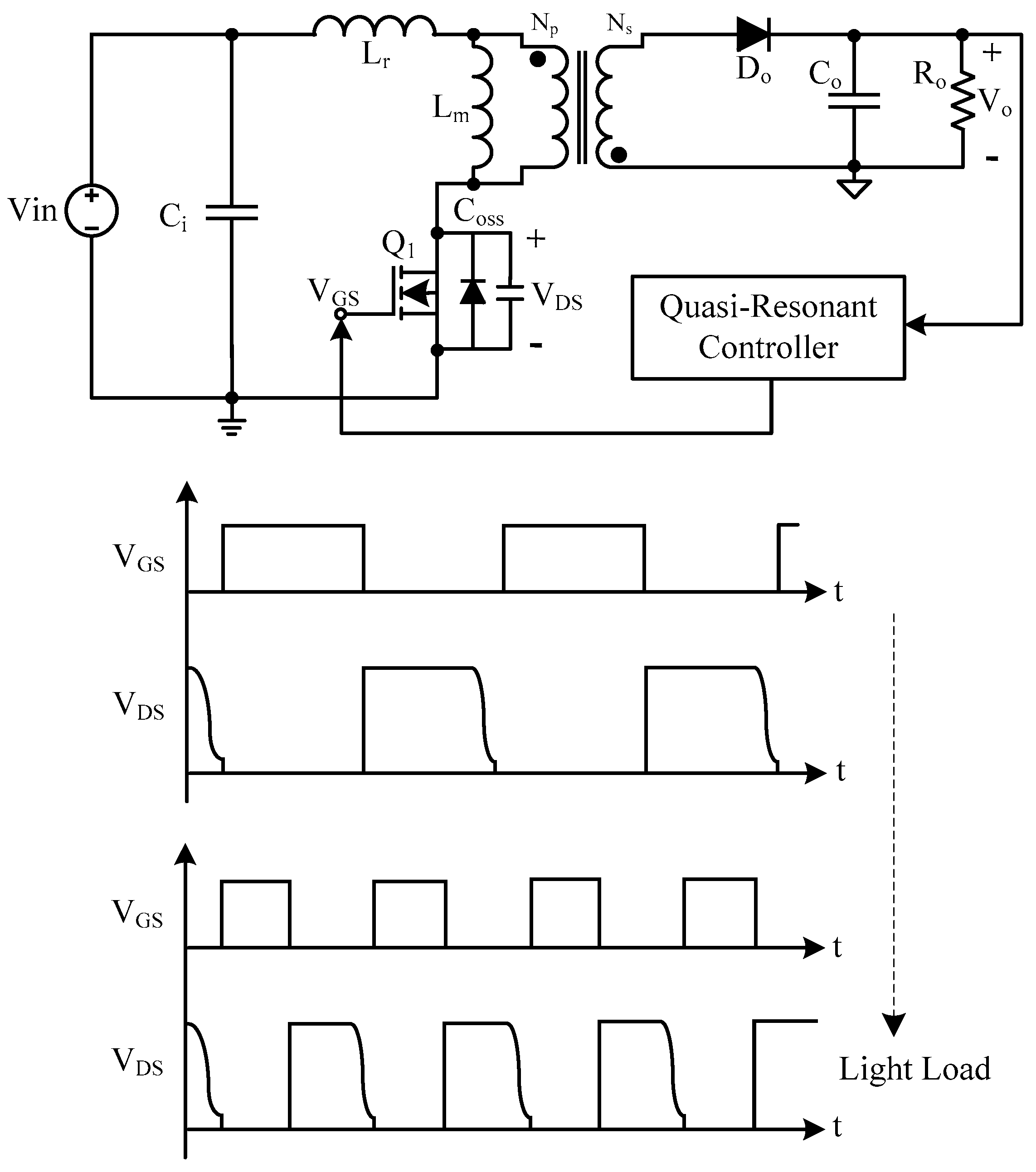
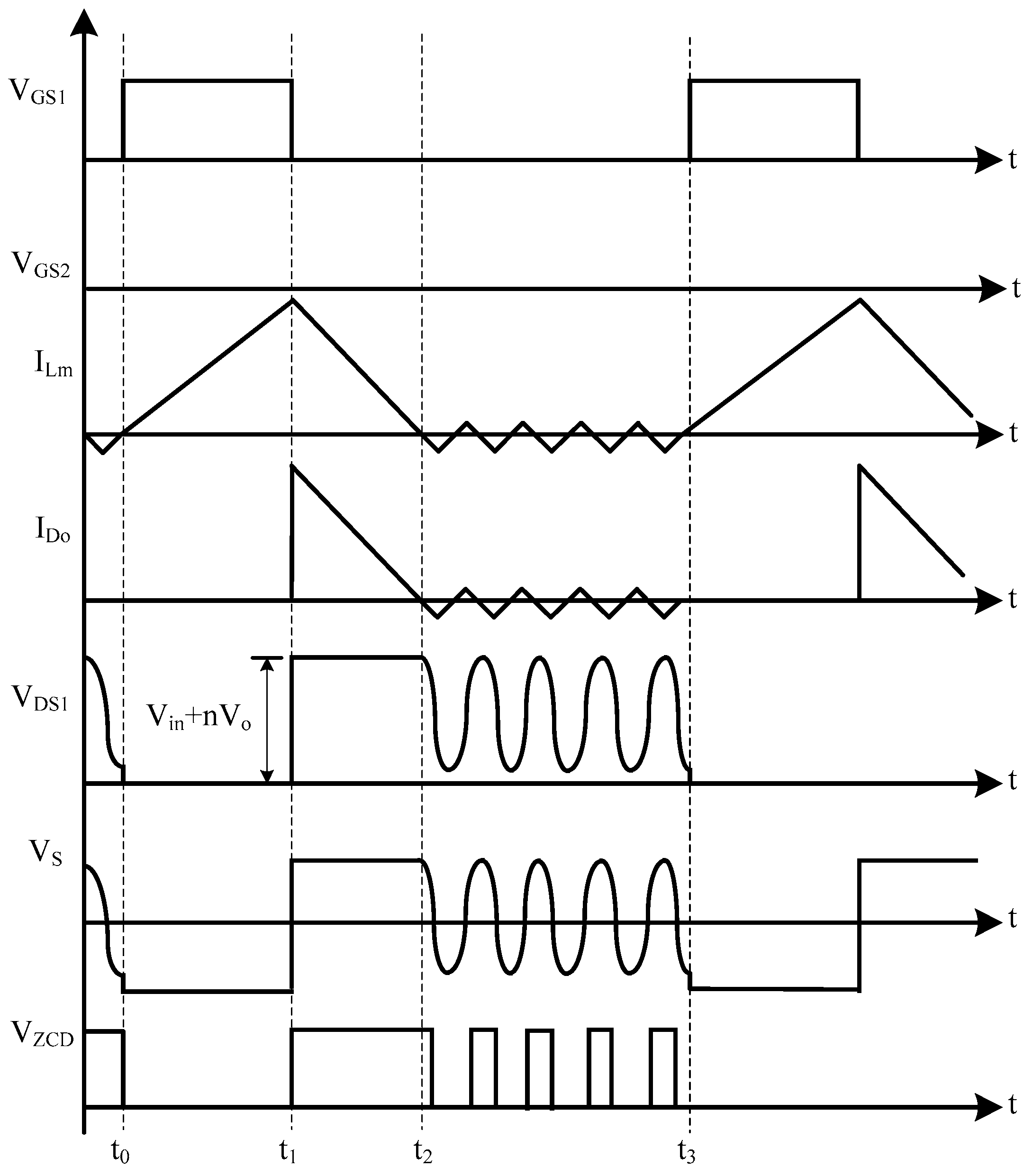
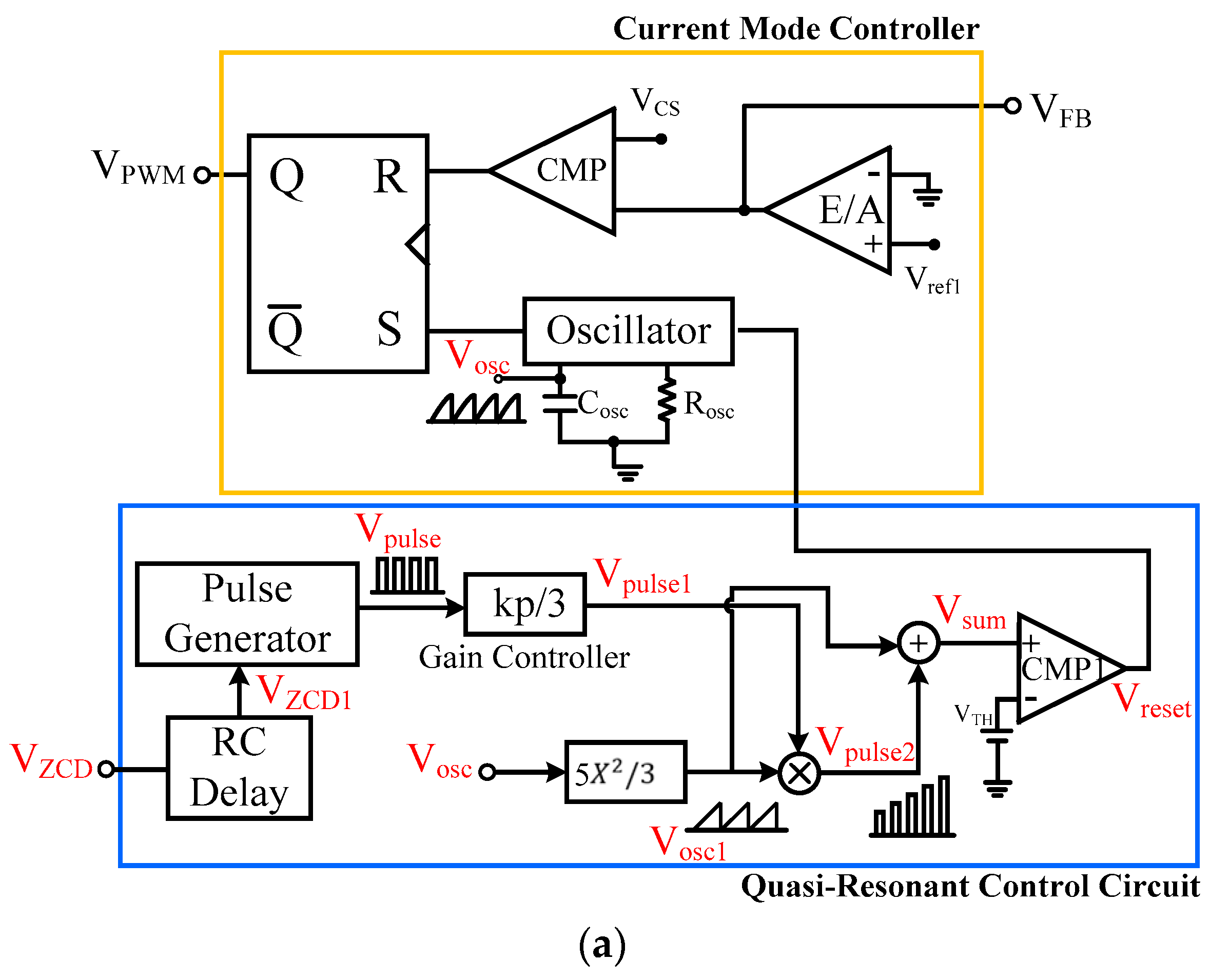
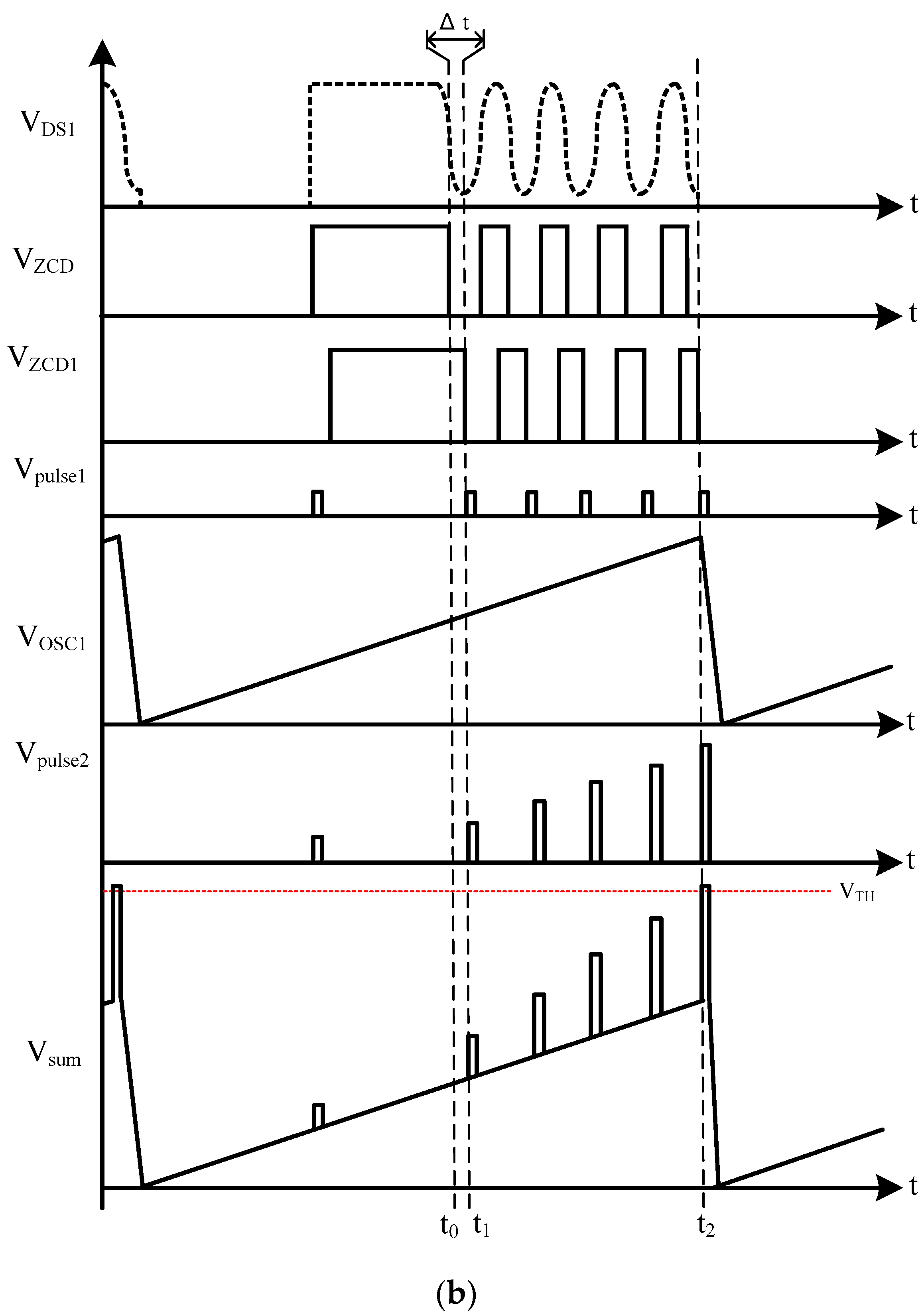
2.2.2. Proposed QR Control Circuit

Before introducing the QR control technique proposed in this paper, the disadvantages of the conventional QRF converter are discussed. Conventional QR control methods rely on the phenomenon of resonance generated by the parasitic capacitance of the main switch and the magnetizing inductance of the transformer to turn on the main switch at the first resonance valley, which can reduce switching loss. However, as the output load increases, the switching frequency also increases, which leads to canceling out the advantages of VS as illustrated in Figure 5.
One popular solution to overcome these inadequacies is the use of a frequency-limiting mechanism. In this paper, a control technology similar to that in [13] is adopted in which only pulse signals are used to adjust the maximum frequency of the oscillator. The operating principle of the proposed converter is divided into two parts: the operating principle of the ACF converter operating in the QR mode and the operating principle of the QR control circuit that limits the maximum switching frequency.
  • The operating principle of the ACF converter operating in the QR mode:
The operating principle of the ACF converter in the QR mode is described as follows. This operation mode is divided into three states as shown in Figure 6, and the complete key waveforms are presented in Figure 7. The following assumptions are used to simplify the analysis:
  • The main switch (Q1) and the auxiliary switch (Q2) have no leakage current and forward resistance;
  • The leakage inductance (Lr) is negligible;
  • The parasitic capacitances, Coss1 and Coss2, are much smaller than Cclamp;
  • Non-ideal characteristics, such as the forward voltage drop and the resistance effect of the secondary-side rectifier diode, are ignored;
  • The output capacitance is large enough to be considered as a constant voltage source;
  • The turn ratio n = Np/Ns.
State 1 (t0 ≤ t < t1):
When t = t0, the main switch (Q1) is turned on, and the auxiliary switch (Q2) is turned off. The input source begins to supply energy to the transformer, and the magnetizing inductor current (ILm) increases linearly. Since the primary and secondary sides of the transformer have opposite polarity, the output rectifier diode (Do) is reverse-biased. The output energy is supplied by the output filter capacitor (Co). The detailed current path is presented in Figure 6a. For the auxiliary winding on the secondary side of the transformer, the voltage VZCD remains low because the voltage VS is less than zero.
State 2 (t1 ≤ t < t2):
When t = t1, the main switch (Q1) and the auxiliary switch (Q2) are turned off. At this time, the magnetizing inductance (Lm) then begins to charge the parasitic capacitor (Coss1) of the main switch (Q1). As a result, the drain-source voltage (VDS) of Q1 on the primary side of the transformer increases rapidly. When VDS1Vin + nVo, the diode, Do, conducts. The energy stored in the transformer is then transferred to the output capacitor and the output load. The detailed current path is shown in Figure 6b. For the auxiliary winding on the secondary side of the transformer, the voltage VZCD changes from low to high due to the transient transition of Vs.
State 3 (t2 ≤ t < t3):
When t = t2, the energy stored in the transformer has been completely transferred to the secondary side, and the current IDo decreases to zero. The converter is thus operating in the discontinuous conduction mode (DCM). The magnetizing inductor (Lm) and the parasitic capacitor (Coss1) begin to resonate. The detailed current path is shown in Figure 6c. In the QR mode, when the voltage drops to the valley, the main switch (Q1) turns on to reduce switching loss. At this time, the output energy is provided to the load by the output filter capacitor (Co). The auxiliary winding on the secondary side of the transformer is in the resonant state due to the voltage Vs, resulting in a square wave signal at the output of the comparator with the same resonant frequency.
  • The operating principle of the QR control circuit with the maximum switching frequency-limiting function:
This section explains the operating principle of the QR control circuit with the maximum switching frequency-limiting function. Figure 8 depicts the QR control block with the maximum switching frequency-limiting function and related key waveforms. Notably, the circuit only operates when the ACF converter is in the resonant state. When voltage VDS1 resonates through point 0 at t0, the voltage VZCD transiently changes from high to low. After being processed by the RC delay circuit, the voltage VZCD1 will be delayed for a period Δt. The falling edge of this square wave may coincide with the valley of the switching voltage VDS. Therefore, the pulse generator and the gain controller can generate an adjustable pulse signal Vpulse1 at time t1. To control the maximum switching frequency limit, the original oscillator signal (VOSC) must be obtained from the current mode controller. After processing by the squarer, this signal becomes a triangular signal at the same frequency, VOSC1. This method is used to accentuate the peak voltage of VOSC. The multiplier is the main focus of this control strategy. The input voltages of the multiplier are VOSC1 and Vpulse1; thus, the peak value of the output voltage Vpulse2 gradually increases. Finally, the voltage Vsum is generated by adding VOSC1 to Vpulse2. As the number of resonances increases, the peak value of Vsum also increases. When the voltage value of Vsum is higher than the reference voltage VTH of comparator CMP1 at t2, the output signal Vreset of CMP1 triggers the current mode controller to reset the oscillator. This technique enables the converter to achieve maximum switching frequency limiting. Thus, controlling the magnitude of the reference voltage VTH determines the valley point of the converter.

3. Design of the Proposed Novel Dual-Mode ACF Converter

The converter structure and operating principles have been described in detail in the previous section. This section describes the design of the proposed dual-mode ACF converter. A 65 W power supply is used in the following example calculations and the description of the component design of the converter. The specifications of the prototype converter are listed in Table 1.
In the following, the design procedure of the converter is briefly presented.
Step 1:
Given that the maximum output power Po,max = 65 W and the efficiency η = 0.9, the magnetizing inductance (Lm) of the transformer can be determined [15]:
L m = η × ( V i n , m i n × D m a x ) 2 2 × f s w × P o , m a x = 409   μ H
Step 2:
After the magnetizing inductance (Lm) of the transformer is known, the peak current of the transformer primary side winding can be calculated:
I p p = P o , m a x η × V i n × D m a x + V i n , m i n × D m a x 2 × L m × f s w 2.357   A  
Step 3:
The maximum output power (Po,max) of the converter is 65 W, and the switching frequency is 65 kHz. In this paper, the PQ26/20 iron core produced by TDK (Tokyo, Japan) was used to calculate the primary winding turns of the transformer. Based on the actual design considerations, the magnetizing inductance (Lm) is 400 μH. From the core datasheet, the effective cross-sectional area of the core (Ae) is 1.19 cm, and the maximum magnetic flux density (Bmax) is 2000 G. The primary winding turns of the transformer (Np) can be calculated as follows:
N p = L m × I p p A e × B m a x × 10 8 39  
Step 4:
The secondary winding turns (Ns) can also be calculated:
N s = V o × ( 1 D m a x ) × N p V i n × D m a x 7  
Step 5:
The output diode must be selected considering the maximum output current and the withstand voltage. The withstand voltage and withstand current of the diode are calculated as follows:
V D , m a x = V i n , m a x N p N s + V o 46.82   V  
I s e c , p e a k = I L , p e a k × n 13.22   A
I s e c , r m s = I s e c , p e a k 1 D m a x 3 5.912   A
In accordance with the results of Equations (5)–(7), the ultrafast rectifier diode BYV32E-150 produced by NXP Semiconductors (Eindhoven, Netherlands) was selected as the output rectifier diode with a peak reverse voltage of 150 V and a peak forward current of 20 A.
Step 6:
To achieve ZVS for the ACF converter power switch, enough energy must be stored in the resonant inductance (Lr) to completely discharge the parasitic capacitance (Cr) of the power switch; the calculations of this energy are as follows:
E L r E C r  
( I p p ) 2 × L r C r × ( V i n + n × V o ) 2
where ELr and ECr are resonant inductance energy and parasitic capacitance energy, respectively.
Step 7:
After the resonant inductance has been determined, the appropriate value of the clamping capacitor (Cclamp) can be calculated as follows:
C c l a m p = ( 1 D m a x ) 2 π 2 × L r × f s w  

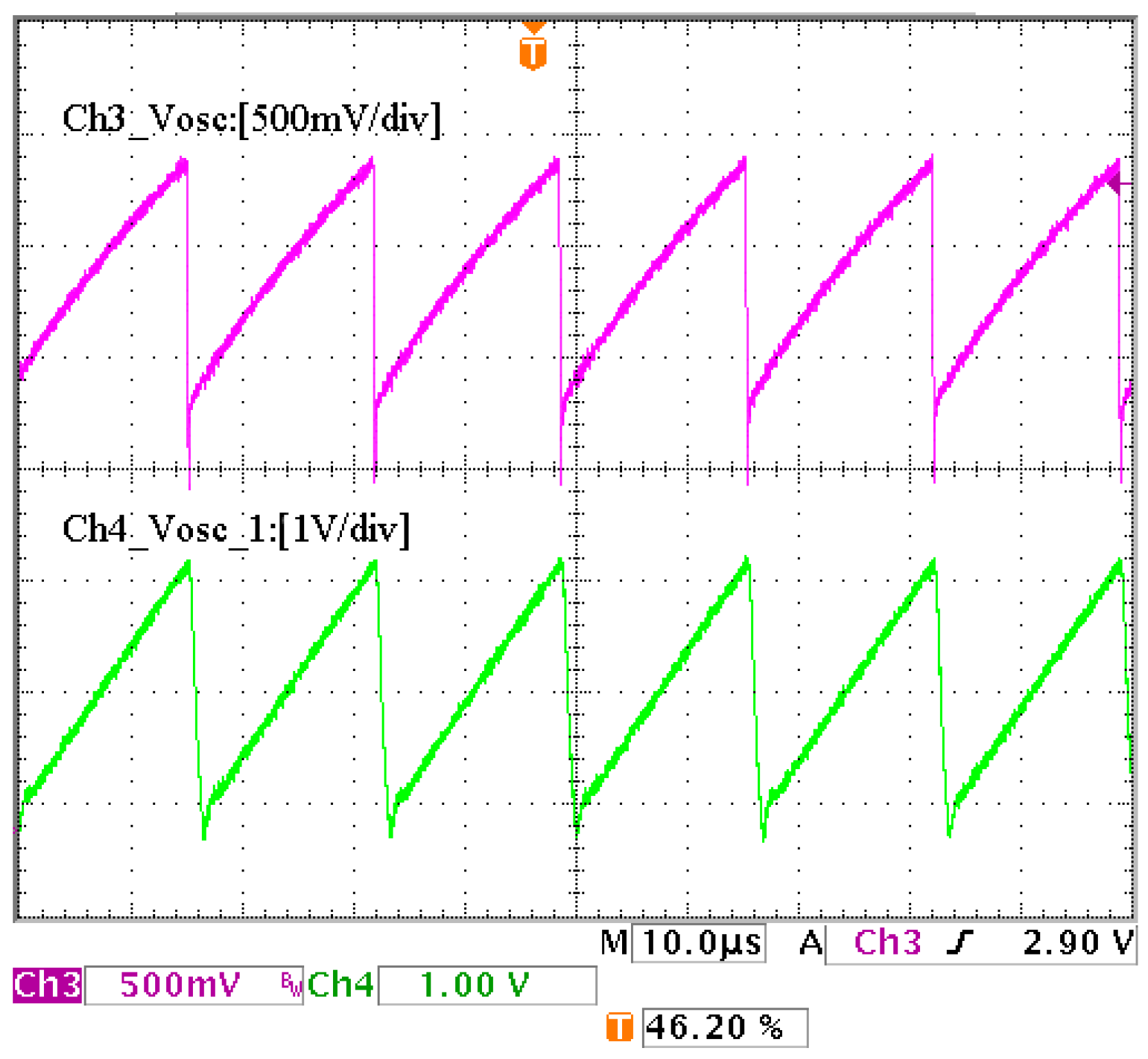
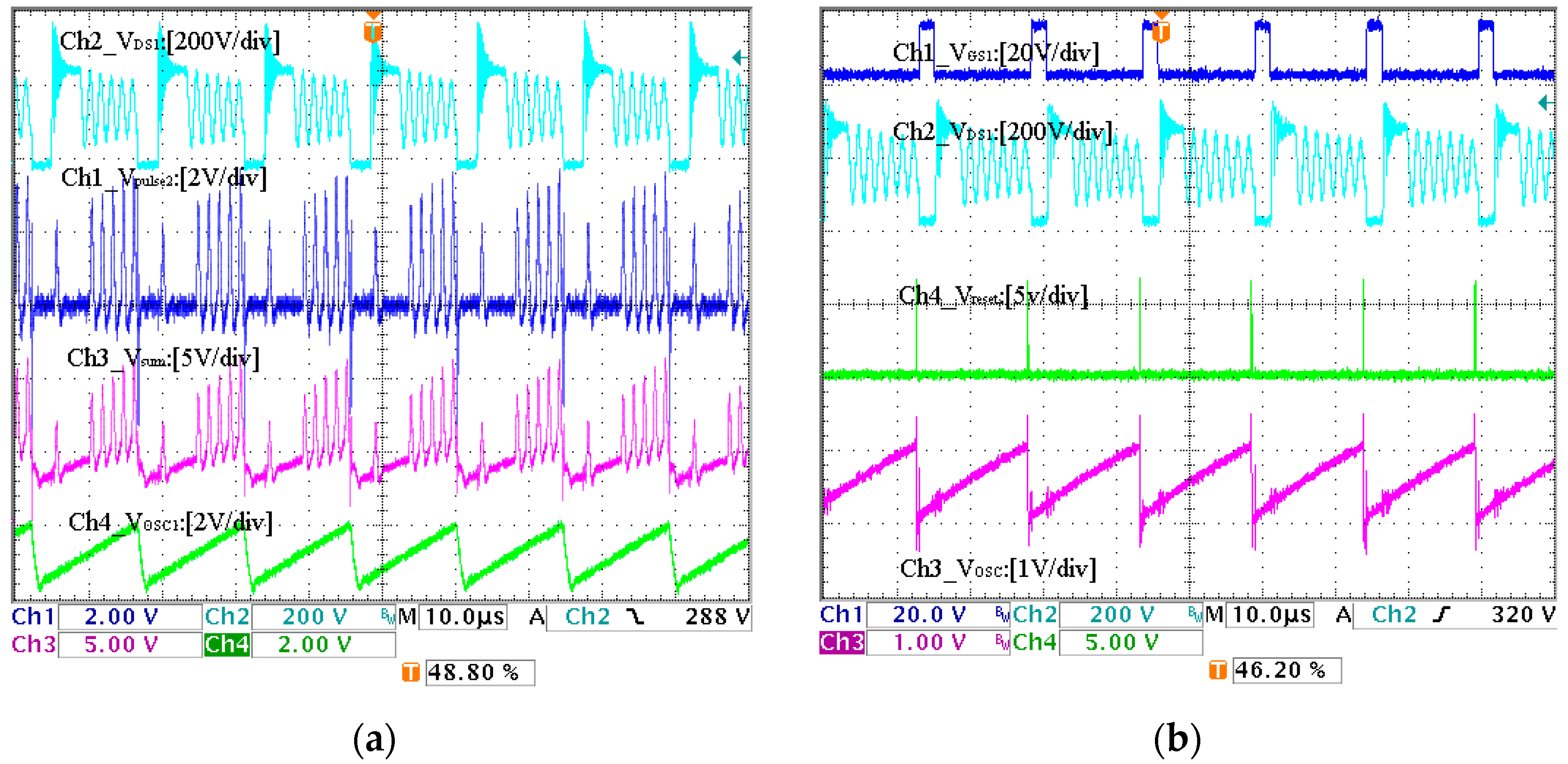
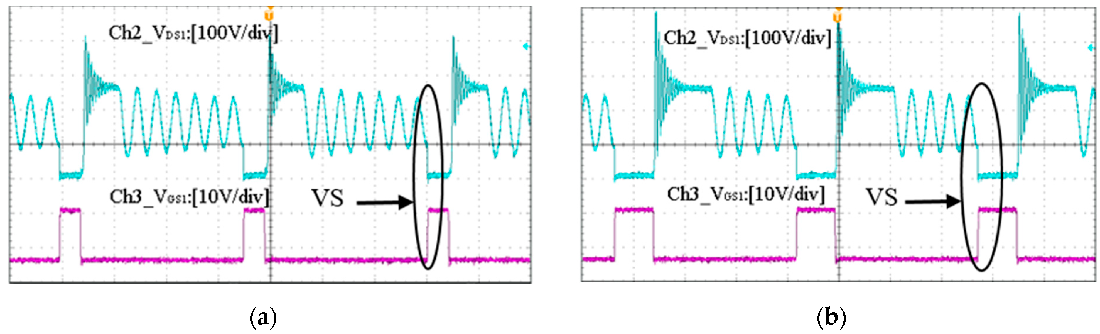
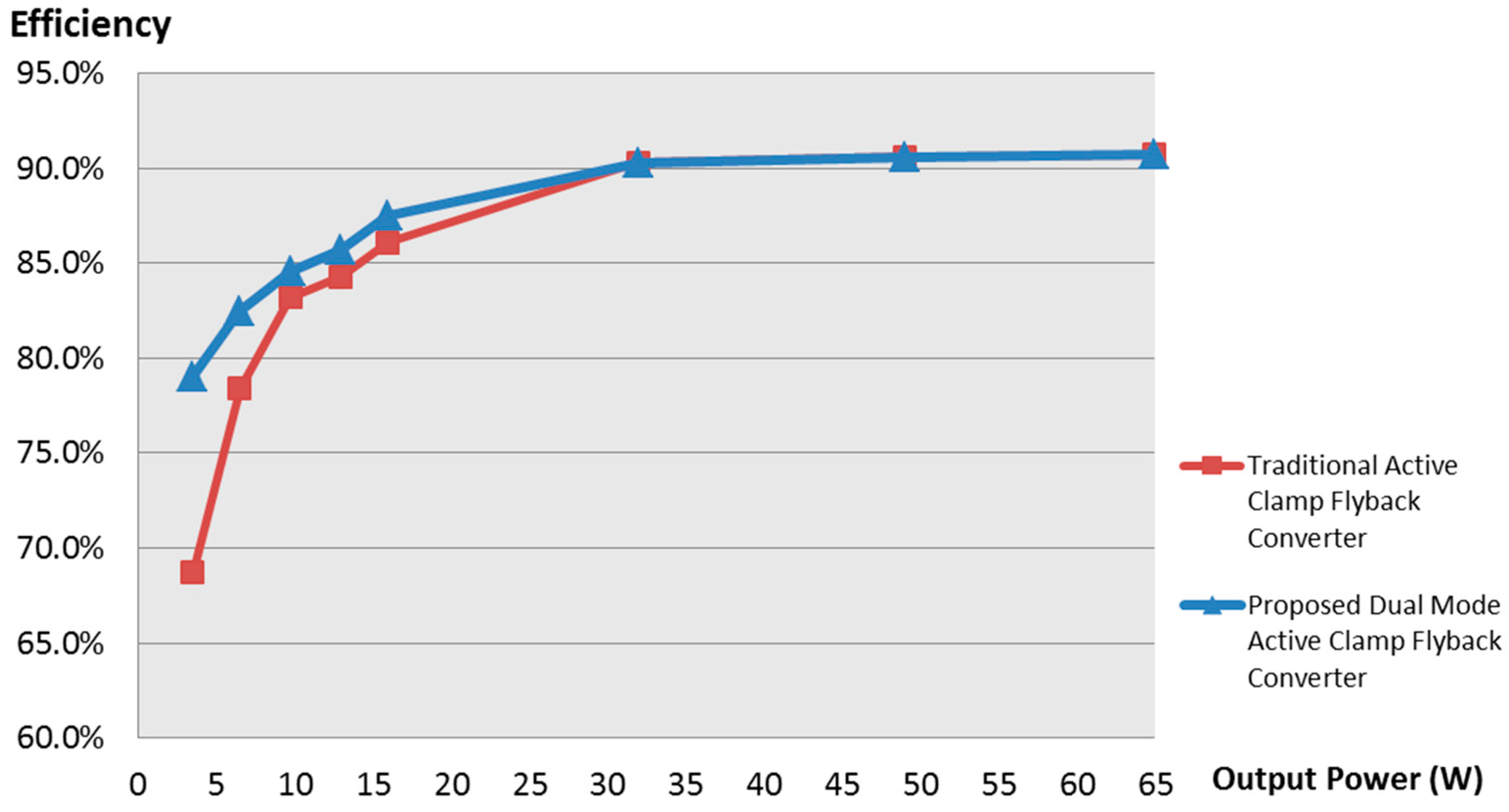
4. Experimental Results

In this experiment, the control IC UC3843 was used as the main controller. The proposed dual-mode ACF converter had the following specifications: the input voltage was 155 VDC, the output voltage was 19 VDC, and the maximum output power was 65 W. The experimental data included the measured critical switching waveforms, control signal waveforms, dual-mode switching waveforms, ZVS waveforms, and other key parameters. Finally, the comparison of efficiency between the conventional ACF converter and the proposed dual-mode ACF converter is presented in this section. The slope shape of the oscillator waveform is critical for the control technique proposed in this paper, because more precise slope changes result in more accurate VS. Generally, the traditional oscillator is an RC circuit; thus, the slightly curved slope causes the failure of frequency-limited VS. To overcome this challenge, a squarer was used to convert the oscillator waveform into a triangular waveform with a linear slope, improving the accuracy of VS. The relevant waveform is presented in Figure 9.
Figure 10a shows that when the voltage VDS1 voltage starts to resonate generating a valley, a voltage pulse signal is generated. Through the multiplier, a linearly rising voltage pulse signal Vpulse2 is then generated. Next, the oscillating voltage signal VOSC1 and the voltage signal Vpulse2 are added by the adder to generate the voltage signal Vsum. Finally, the voltage signal Vsum is compared with the reference voltage VTH to generate a reset voltage signal Vreset, which restarts the control IC UC3843 to complete the frequency-limiting VS as shown in Figure 10b. In other words, the voltage level of the reference voltage VTH determines the VS point, and higher VTH values cause a slower system switching frequency. Conversely, lower VTH causes a faster system switching frequency.
Figure 11 presents the key voltage waveforms of the converter operating at different output powers. If the converter operates was at an output power of 6.5 W, the switching frequency of the converter was approximately 70 kHz as presented in Figure 11a. For an output power of 19.5 W, the switching frequency of the converter decreased to approximately 68 kHz as presented in Figure 11b. Although the output power of the converter varied, the switching frequency of the circuit can be limited within a fixed range by the frequency-limiting QR control function of the QR control circuit proposed in this paper. If the output power increased above 19.5 W, the converter changed the operation mode from the QR to the active-clamp mode as presented in Figure 12. Figure 13 shows the ZVS waveforms of the power switches of the proposed converter. The figure shows that before the main switch (Q1) was turned on, the drain-source voltage of the main switch VDS1 decreased to zero. The same principle was applied to the auxiliary switch (Q2); thus, both power switches achieved ZVS.
Figure 14 presents the key waveforms for switching between the two modes of the converter according to the change in output power when the input voltage Vin = 155 VDC. If the output power was 6.5 W, the driving signal VGS2 of the auxiliary switch (Q2) was off, and the driving signal VGS1 of the main switch (Q1) adjusted the pulse width modulation in accordance with the load. At this time, the converter operated in the QR mode. If the output power increased from 6.5 to 65 W, the drive signal VGS2 of the auxiliary switch (Q2) entered a working state, and the main switch (Q1) and the auxiliary switch (Q2) operated in a complementary manner to enable the converter to operate in the active-clamp mode as presented in Figure 14a. By contrast, if the output power decreased from 65 to 6.5 W, the driving signal VGS2 of the auxiliary switch (Q2) changed from the working state to the off state, and the operation mode of the converter changed from the active-clamp mode to the QR mode as shown in Figure 14b. These experimental data demonstrated that the converter proposed in this paper can switch between the two modes.
Table 2 presents the efficiency measurement data for the dual-mode ACF converter. In the table, input current, output current, output voltage, and efficiency are presented under different load conditions with a voltage of 155 VDC as the input power supply. Figure 15 provides a comparison of the efficiency curves of the conventional ACF converter and the dual-mode ACF converter at different output power levels. The curve comparison diagram reveals that for an output power of 3.5 W, the efficiency difference between the two converters is at a maximum of 11%. If the output load increases, conduction losses gradually increase; thus, the efficiency difference between the two converters decreases. Table 2 and Figure 15 show that the control technique proposed in this paper has good performance under light load conditions. In addition, Table 3 presents the load regulation measurement data. Based on the measurement results, it can be seen that the minimum load regulation value is 1.09% at the output power of 65 W (i.e., full load).

5. Conclusions

This paper presented a new dual-mode switching control strategy for the ACF converter working in DCM, which can switch to the QR mode at light loads to improve overall efficiency. This paper proposed a new dual-mode switching control strategy for an ACF converter operating in DCM to enable operation in the QR mode under light load to optimize the overall operation. The control techniques and operating principles were described in detail. The operating principles and the results of an analysis of the control techniques were carefully discussed. A prototype of the 65 W dual-mode ACF converter was developed, and experiments provided satisfactory results. Experimental results revealed that the auxiliary switch of the resonant tank closed when the dual-mode ACF converter was under light load, which enabled the main switch to perform VS and achieve QR mode control. On the contrary, the converter operated in the active-clamp mode under medium and heavy load conditions, thereby achieving ZVS for both power switches to maintain the high efficiency of conventional ACF. In other words, the proposed dual-mode ACF converter uses QR mode VS characteristics to improve the poor efficiency of conventional ACF under light load. However, the switching frequency of the QR mode is critical to determining the light load efficiency. In general, it is recommended to design the QR mode switching frequency as close to the active-clamp mode switching frequency as possible, because excessively high switching frequencies increase switching losses at light loads. This proposed dual-mode control ACF topology is suitable for applications with relatively low power consumption (under 200 W).

Author Contributions

Conceptualization, J.-M.W. and T.N.T.T.; methodology, H.-C.W. and J.-M.W.; validation, T.N.T.T., H.-C.W. and J.-M.W.; resources, J.-M.W.; writing—original draft preparation, J.-M.W. and T.N.T.T.; writing—review and editing, J.-M.W. and T.N.T.T. All authors have read and agreed to the published version of the manuscript.

Funding

This research was funded by the Ministry of Science and Technology, R.O.C. (grant number: MOST 110-2622-E-150-002).

Data Availability Statement

Not applicable.

Conflicts of Interest

The authors declare no conflict of interest.

References

  1. Watson, R.; Hua, G.C.; Lee, F.C. Characterization of an active clamp flyback topology for power factor correction applications. IEEE Trans. Power Electron. 1996, 11, 191–198. [Google Scholar] [CrossRef]
  2. Watson, R.; Lee, F.C.; Hua, G.C. Utilization of an active-clamp circuit to achieve soft switching in flyback converters. IEEE Trans. Power Electron. 1996, 11, 162–169. [Google Scholar] [CrossRef]
  3. Papanikolaou, N.P.; Tatakis, E.C. Active voltage clamp in flyback converters operating in CCM mode under wide load variation. IEEE Trans. Power Electron. 2004, 51, 632–640. [Google Scholar] [CrossRef]
  4. Liu, P.-H. Design consideration of active clamp flyback converter with highly nonlinear junction capacitance. In Proceedings of the 2018 IEEE Applied Power Electronics Conference and Exposition (APEC), San Antonio, TX, USA, 4–8 March 2018; pp. 783–790. [Google Scholar]
  5. Wu, S.-T.; Cheng, Y.-T. Design and Implementation of a Single-Stage PFC Active-Clamp Flyback Converter with Dual Transformers. Electronics 2021, 10, 2588. [Google Scholar] [CrossRef]
  6. Leng, C.-M.; Chiu, H.J. Three-Output Flyback Converter with Synchronous Rectification for Improving Cross-Regulation and Efficiency. Electronics 2021, 10, 430. [Google Scholar] [CrossRef]
  7. Medina-Garcia, A.; Schlenk, M.; Morales, D.P.; Rodríguez, N. Resonant Hybrid Flyback, a New Topology for High Density Power Adaptors. Electronics 2018, 7, 363. [Google Scholar] [CrossRef] [Green Version]
  8. Jung, J.; Ahmed, S. Flyback converter with novel active clamp control and secondary side post regulator for low standby power consumption under high-efficiency operation. IET Power Electron. 2011, 4, 1058–1067. [Google Scholar] [CrossRef]
  9. Kim, J.h.; Ryu, M.-H.; Min, B.d.; Song, E.-H. A Method to Reduce Power Consumption of Active-Clamped Flyback Converter at No-Load Condition. In Proceedings of the IECON 2006—32nd Annual Conference on IEEE Industrial Electronics, Paris, France, 6–10 November 2006; pp. 2811–2814. [Google Scholar]
  10. Wang, C.; Xu, S.; Shen, W.D.; Lu, S.L.; Sun, W.F. A Single-Switched High-Switching-Frequency Quasi-Resonant Flyback Converter. IEEE Trans. Power Electron. 2019, 34, 8775–8786. [Google Scholar] [CrossRef]
  11. Li, J.T.; van Horck, F.B.M.; Daniel, B.J.; Bergveld, H.J. A High-Switching-Frequency Flyback Converter in Resonant Mode. IEEE Trans. Power Electron. 2017, 32, 8582–8592. [Google Scholar] [CrossRef]
  12. Park, H.P.; Jung, J.H. Design Methodology of Quasi-Resonant Flyback Converter With a Divided Resonant Capacitor. IEEE Trans. Power Electron. 2021, 68, 10796–10805. [Google Scholar] [CrossRef]
  13. Wang, J.; Lin, C.-W.; Huang, K.-Y.; Wong, J.-S. The Novel Quasi-Resonant Flyback Converter With Autoregulated Structure for Parallel/Serial Input. IEEE Trans. Power Electron. 2020, 67, 992–1004. [Google Scholar] [CrossRef]
  14. Jeng, S.-L.; Peng, M.T.L.; Hsu, C.Y.; Chieng, W.-H.; Shu, J.P.H. Quasi-resonant flyback DC/DC converter using GaN power transistors. World Electr. Veh. J. 2012, 5, 567–573. [Google Scholar] [CrossRef] [Green Version]
  15. Pressman, A.I. Switching Power Supply Design; McGraw-Hill: New York, NY, USA, 1998. [Google Scholar]
Figure 1. Flyback converter topology.
Electronics 11 01308 g001
Figure 2. (a) Active-clamp flyback converter structure and key waveforms; (b) quasi-resonant flyback converter structure and key waveforms.
Electronics 11 01308 g002
Figure 3. (a) Dual-mode control strategy proposed in this paper; (b) sequence diagram of the key waveform under light load; (c) sequence diagram of the key waveform under heavy load.
Electronics 11 01308 g003aElectronics 11 01308 g003b
Figure 4. Dual-mode switching circuit structure.
Electronics 11 01308 g004
Figure 5. Quasi-resonant flyback converter structure and key waveforms correspond to load conditions.
Electronics 11 01308 g005
Figure 6. (ac) Three operating states of the ACF converter in the QR mode.
Electronics 11 01308 g006
Figure 7. Key waveforms of the ACF converter operating in the QR Mode.
Electronics 11 01308 g007
Figure 8. (a) QR control block with the maximum switching frequency-limiting function and (b) key waveform sequence diagram.
Electronics 11 01308 g008aElectronics 11 01308 g008b
Figure 9. Oscillator waveform with (Ch4) and without (Ch3) the frequency-limiting control mechanism.
Electronics 11 01308 g009
Figure 10. (a) Power switch voltage waveform and its generated signal waveforms; (b) key control signal waveforms of the proposed ACF converter in QR mode.
Electronics 11 01308 g010
Figure 11. Key voltage waveforms of the proposed ACF converter operating at (a) 6.5 W and (b) 19.5 W. The converter is in the QR mode.
Electronics 11 01308 g011
Figure 12. Waveforms of the main switch and auxiliary switch of the proposed ACF converter under medium- to full-load conditions (above 19.5 W). The converter is in the active-clamp mode.
Electronics 11 01308 g012
Figure 13. ZVS waveforms of the power switches of the proposed ACF converter in the active-clamp mode.
Electronics 11 01308 g013
Figure 14. Key waveforms of dual-mode switching: (a) QR mode to the active-clamp mode; (b) active-clamp mode to the QR mode.
Electronics 11 01308 g014
Figure 15. Efficiency curves of the conventional ACF converter and dual-mode ACF converters at different output powers.
Electronics 11 01308 g015
Table 1. Specifications of the proposed ACF converter.
ParametersValue
Input voltage, Vin155 V
Maximum output power, Po,max65 W
Output voltage, Vout19 V
Output current, Iout3.42 A
Switching frequency, Fsw65 kHz
Maximum duty cycle, Dmax0.4
Efficiency, η90%
Maximum magnetic flux density, Bmax2000 G
Table 2. Efficiency of the proposed dual-mode ACF converter.
Input Voltage, VinInput Current, IinOutput Voltage, VoOutput Current, IoEfficiency, η
155 V0.030 A19.3 V0.19 A79%
155 V0.052 A19.3 V0.34 A82.5%
155 V0.075 A19.3 V0.51 A84.6%
155 V0.098 A19.3 V0.68 A85.7%
155 V0.119 A19.3 V0.84 A87.5%
155 V0.229 A19.2 V1.67 A90.3%
155 V0.349 A19.2 V2.55 A90.6%
155 V0.464 A19.2 V3.41 A90.7%
Table 3. Load regulation measurement data of the proposed dual-mode ACF converter.
Output Power, PoOutput Voltage, Vo Load Regulation, LR
3.5 W19.289 V1.52%
6.5 W19.303 V1.59%
13.0 W19.304 V1.60%
19.5 W19.305 V1.61%
26.0 W19.293 V1.54%
32.5 W19.258 V1.36%
39.0 W19.236 V1.24%
45.5 W19.226 V1.19%
52.0 W19.227 V1.19%
58.5 W19.222 V1.17%
65.0 W19.207 V1.09%
Publisher’s Note: MDPI stays neutral with regard to jurisdictional claims in published maps and institutional affiliations.

