Article

Investigation of ON-State Breakdown Mechanism in AlGaN/GaN HEMTs with AlGaN Back Barrier

1
R&D Center of High-Frequency & High-Voltage Device and Integrated Technology, Institute of Microelectronics of Chinese Academy of Sciences, Beijing 100029, China
2
University of Chinese Academy of Sciences, Beijing 100049, China
*
Author to whom correspondence should be addressed.
Electronics 2022, 11(9), 1331; https://doi.org/10.3390/electronics11091331
Submission received: 21 March 2022 / Revised: 18 April 2022 / Accepted: 19 April 2022 / Published: 22 April 2022
(This article belongs to the Special Issue Semiconductor and Package for Next Generation)

Abstract

:
The temperature-dependent ON-state breakdown B V O N loci of AlGaN/GaN high-electron-mobility transistors (HEMTs) with an AlGaN back barrier were investigated using the gate current extraction technique. The impact ionization of acceptor-like traps was revealed to be responsible for the ON-state breakdown in HEMTs as a 2D electron gas (2DEG) channel is marginally turned on. The characteristic electric field E i of impact ionization was extracted, exhibiting a U-shaped temperature dependence from 40 to −30 C, with minimum E i occurring at −10 C. The impurity scattering effect of acceptor-like traps in AlGaN/GaN heterostructures is suggested to be responsible for the negative temperature dependence of B V O N and E i below −10 C.

1. Introduction

GaN-based high-electron-mobility transistors (HEMTs) are especially attractive for next-generation RF/microwave power amplifiers and power switching applications, as a result of their high breakdown electric field and polarization-induced high-mobility, as well as high-density 2D electron gas (2DEG) at the AlGaN/GaN hetero-interface [1,2,3,4]. Intensive efforts have been dedicated to the mechanism of the three-terminal OFF-state breakdown B V O F F characteristics that determine the power range of GaN-based power devices [5,6,7,8]. However, limited works have reported on the investigation of the ON-state breakdown B V O N mechanism in AlGaN/GaN HEMTs, although the high power state of high current and high voltage is typically an intermediate state for both RF power amplifiers in large-signal operation and power switches in the switching process of turn-ON and turn-OFF [9,10,11]. Moreover, the ON-state breakdown mechanism is also beneficial to the definition and design of the safe operation area (SOA) in GaN-based power devices. In addition, to improve the 2DEG confinement and breakdown characteristics of GaN-based HEMTs, a low-Al-composition AlGaN back barrier is commonly introduced in the epitaxial structure of AlGaN/GaN heterostructures [12,13,14], while its influence on the trapping behavior deserves further exploration.
To determine B V O N , the typical approach is to increase the drain voltage of the devices, for a given gate bias, until a significant rise in the drain current is observed [15]. Although such a characterization method is precise, it is destructive and not suitable for breakdown mechanism study, which usually requires reproducible measurements [16,17]. In this regard, Somerville et al. developed a gate current extraction technique and applied it to study the ON-state breakdown of InAlAs/InGaAs HEMTs [18]. Such a non-destructive method is rarely used for the characterization of GaN-based HEMTs’ ON-state breakdown except for GaN MESFETs [19].
In this work, the ON-state breakdown loci of AlGaN/GaN HEMTs with an AlGaN back barrier were studied with the gate current extraction technique, and the impact ionization of acceptor-like traps was observed within the temperature range from 40 to −30 C. The characteristic electric field E i of impact ionization of traps was extracted, exhibiting a U-shaped temperature dependence, and the underlying physical mechanism was investigated.

2. Device Fabrication

The GaN-on-SiC HEMT wafer used in this work was grown by MOCVD on a 2-inch SiC substrate. The epitaxial layer structure was GaN cap (∼2 nm)/barrier-Al 0.21 0.21Ga 0.79 N (∼25 nm)/interlayer-AlN (∼1 nm)/channel-GaN (∼50 nm)/buffer-Al 0.04 Ga 0.96 N (1 μ m)/buffer—GaN (1 μ m)/nucleation-AlN (∼100 nm). Note that the 1 μ m Al 0.04 Ga 0.96 N back barrier was used to realize a better 2DEG confinement. The sheet density of the 2DEG, as determined by capacitance–voltage measurement, was 7.2 × 10 13 cm 2 . The typical 2DEG sheet resistance at room temperature, as determined by the transfer length method, was about 325 Ω /sq. The contact resistivity was 0.8 Ω ·mm, and the specific contact resistivity was 1.22 × 10 6 Ω ·cm 2 .
The fabrication of the AlGaN/GaN HEMTs was started with ohmic contacts formed by an alloyed Ti/Al/Ni/Au metal stack. Then, a 120 nm SiN x was grown at 300 C by PECVD to passivate the surface. After that, device isolation was achieved by multiple-energy nitrogen ion implantation. A 0.35- μ m gate was defined by E-beam lithography, and Ni/Au Schottky gate deposition was applied after dry etching through the PECVD-SiN x layer. The gate width, gate–source, and gate–drain separations were 8 × 100 μ m (multi-finger), 1.25 μ m, and 2.4 μ m, respectively.
The fabricated HEMTs featured a typical threshold voltage V T H of −3.3 V and an extrinsic peak transconductance of 274 mS/mm at 20 C at V D S of 10 V. The OFF-state breakdown voltage was determined to be ∼76 V at a drain leakage current of 0.1 mA/mm. As shown in Figure 1a, the output characteristics show a climbing step on I D S after the device is turned ON, which exhibits as kink behavior. This is probably caused by acceptor-like traps located in the vicinity of the 2DEG channel [20]. The traps are charged at low drain bias, partially depleting the 2DEG in the channel. Then, as the V D S increases, these charged traps may be discharged, caused by hot electrons under high drain bias, resulting in an increasing I D S . This phenomenon can also be observed from the transfer characterizations of the device. As shown in Figure 1b, the gate leakage current I G may increase when the gate voltage changes from −4 to −3 V as a result of the traps’ discharge. Owing to the back barrier effect of the AlGaN buffer, the peak E-field on the drain side of the gate edge will be significantly enhanced, contributing to the effective acceleration of channel electrons. The traps will be discharged by these high-energy electrons through hot electrons [21]. The impact-ionization-induced detrapping behavior was also confirmed by the appearance of bell-shaped features in the gate leakage current at V D S > 6 V, as the device is turned ON during transfer characterizations (Figure 1b). The impact ionization would induce electron–hole pairs with holes captured by the gate electrodes [22,23]. Meanwhile, the impact-ionization-induced detrapping behavior also causes a negative shift of V T H , as shown in Figure 1b.

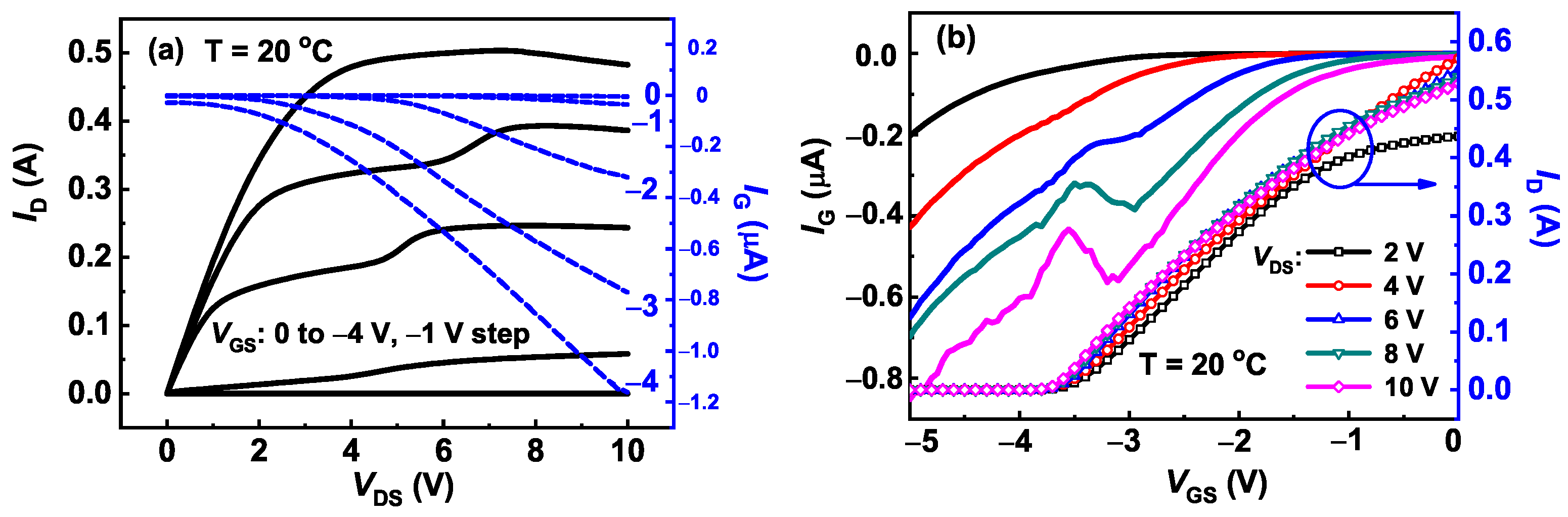
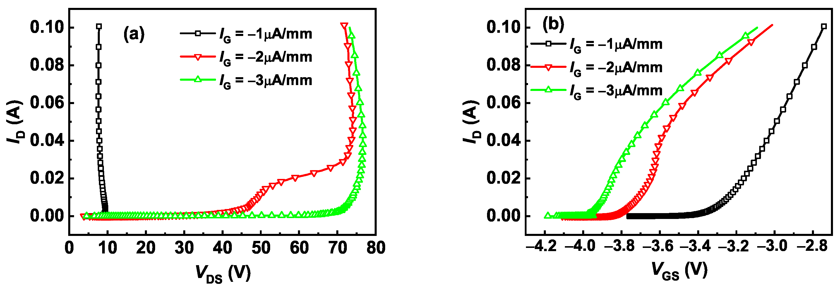
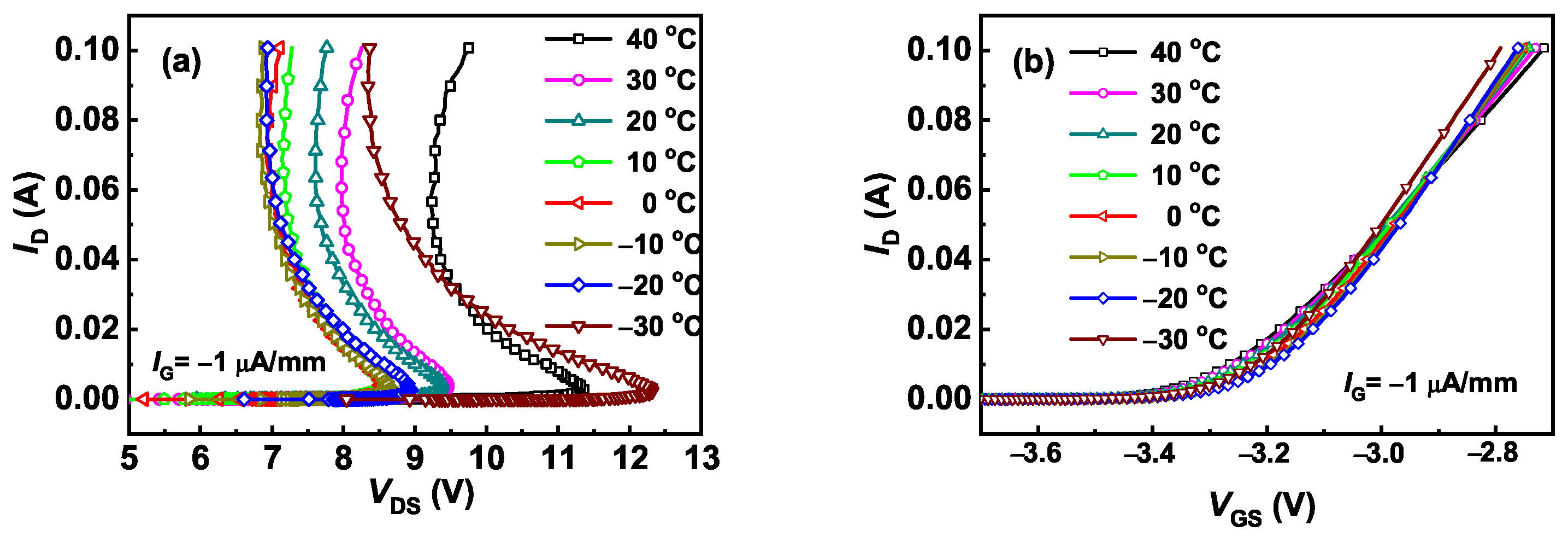
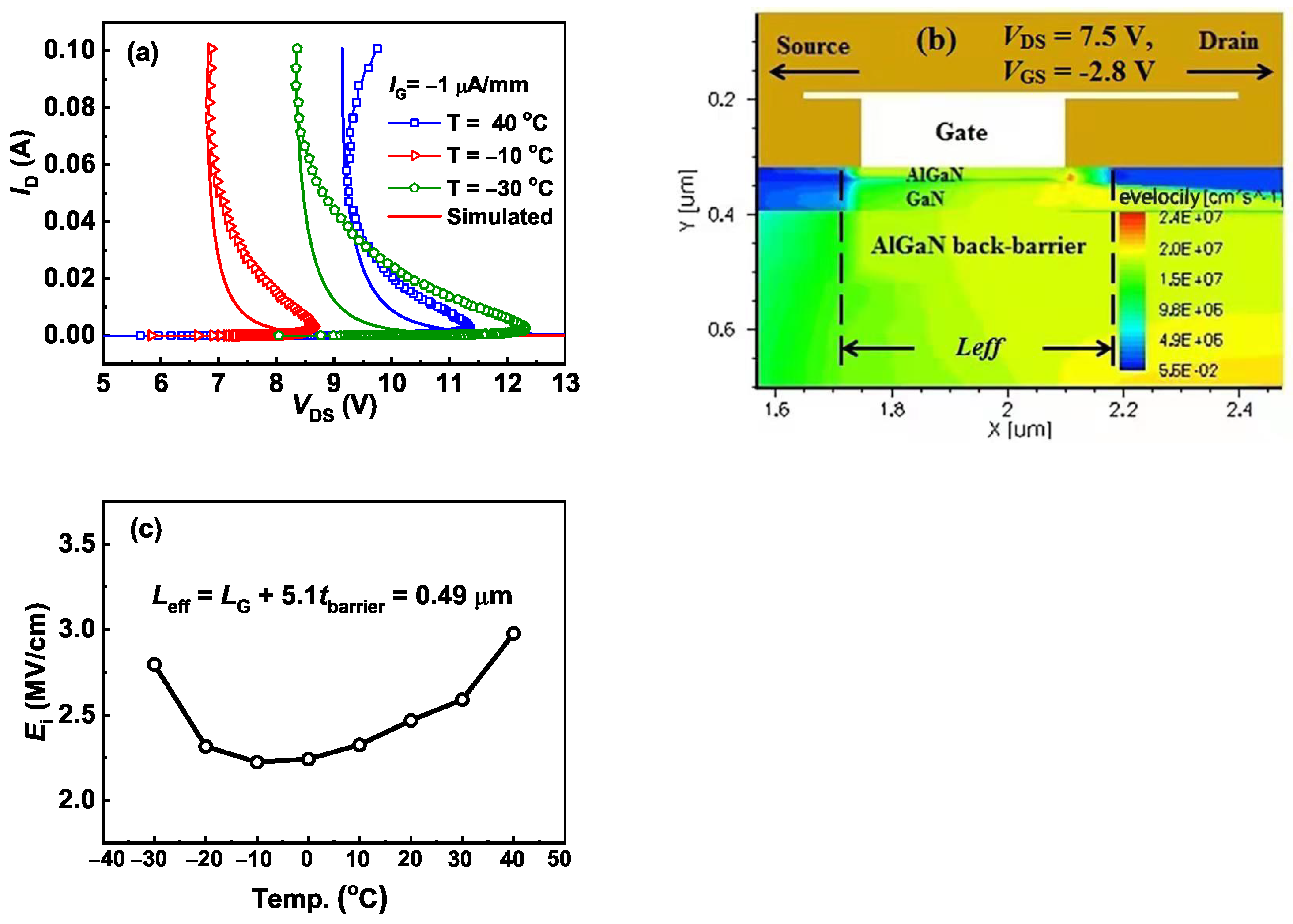
3. ON-State Breakdown and Impact Ionization

The ON-state breakdown loci ( B V O N ) of the fabricated device were measured by the gate current extraction technique, as shown in Figure 2a. The gate current I G was held constant at different predefined values (−1/−2/−3 μ A/mm), and I D was ramped from − I G (OFF-state) to 100 mA (ON-state). The corresponding drain–source ( V D S ) and gate–source voltages ( V G S ) were monitored and shown in Figure 2a,b, respectively. At I G of −1 μ A/mm, the monitored V D S increased rapidly with I D in the OFF-state as V G S was below V T H . The gate leakage current in this region was expected to be dominated by electrons injected from the gate into the channel through thermionic field emission and tunneling, and the increase of the V G S was driven by the increase of the drain current to turn on the channel gradually [23]. Once V G S increased above V T H and turned the device ON, lower drain bias voltage was enough to sustain the drain current, until an upsurge of I D featuring infinite conductance was observed.
The abrupt increase of I D in the ON-state breakdown locus of I G = −1 μ A/mm (Figure 2a) implies that impact ionization takes place near the drain-side gate edge in AlGaN/GaN HEMTs [16,18,19,20,21,22,23,24]. A large amount of holes can thus be generated in this high-field region, and some of them are collected by the gate electrode, contributing a new leakage current component I h o l e , which makes a dominant contribution to I G in the infinite conductance region ( I D versus V D S ) [16]. By increasing the magnitude of I G to −2 and −3 μ A/mm, a higher maximum OFF-state V D S can be reached, as a higher electric field is required to inject electrons to sustain a higher I G [18,19]. However, the maximum ON-state V D S of both I G = −2 and −3 μ A/mm is close to the OFF-state breakdown voltage of the device (∼76 V), and the burnout of the devices occurred after such measurements, probably due to the high power density they suffered. From this point of view, a safe I G of −1 μ A/mm was used to perform reproducible temperature-dependent measurements, through which the ON-state breakdown mechanism can be investigated. On the other hand, the monitored V G S of I G = −2 and −3 μ A/mm exhibited significant negative shift as compared with that of I G = −1 μ A/mm, as shown in Figure 2b. This was likely caused by drain-induced barrier lowering (DIBL) at high drain bias [25].
To verify the impact ionization characteristics in AlGaN/GaN HEMTs, the temperature-dependent ON-state breakdown loci of the fabricated devices were performed from 40 to −30 C, as shown in Figure 3. It shows a rapid degradation of the device’s B V O N properties both at a high and a low temperature, where the high temperature B V O N degradation has been reported as the cause of the impact-ionization-induced hot electrons [10], and the degradation at a low temperature is considered as a result of the carrier mobility decrease. For all the measured temperature, the B V O N loci exhibited similar features except for the different minimum value of B V O N ( B V O N , m i n ). It decreased from 9.3 to 6.8 V from 40 to −10 C and then reversed to increase to 8.4 V as the temperature further decreased to −30 C. Note that a further increase of I D over the infinite conductance region made the B V O N loci bend forward to a higher V D S again. This was due to the reduction of the peak electric field in the gate–drain region (roughly proportional to V D G ) and consequently of the impact ionization rate, as V G S increased further with I D . To maintain a constant I G , a higher V D S was required again [23]. Moreover, the forward bending of B V O N loci became more evident at a higher temperature, since the impact ionization features a negative temperature coefficient.
The impact-ionization-induced hole current I H o l e can be expressed using a classical impact ionization model as follows [16]:
I h o l e = α n ( E ) · I D · L e f f = α 0 · e E i / E · I D · L e f f
where α n ( E ) is the impact ionization rate, L e f f is the characteristic length of high-field region with its upper bound given by L G D , E i is the characteristic electric field, and α 0 is a temperature-dependent coefficient reported by Baliga [26]. As L e f f increased, the average electric field and I D became lower, resulting in a higher B V O N of the device. However, this would lead to other problems such as the rising ON-state resistance of the device in turn, which calls for further research. Assuming that the total gate current I G is dominated by I h o l e in the infinite conductance region, all the measured B V O N loci were simulated with Equation (1), and some of them are shown in Figure 4a. The deviation between the measured and simulated ones in the ON-state region was probably a result of hot-electron-induced de-trapping of acceptor-like traps [6]. This also needs more precise calculation on the parameters especially as the temperature becomes lower. For example, the impact ionization rate α n (E) may be taken as a temperature-dependent parameter, which may be set as α n = 2.82 × 10 6 6.34 × 10 3 T [26], and the effective gate length L e f f may also change at various temperatures as the electron velocity distribution may be different, influenced by carrier mobility. The de-trapping process results in a negative shift of V T H and, thus, increases of I D .
The effective gate length L e f f of the fabricated device was determined to be 0.49 μ m by the formula of L G + 5.1 × t b a r r i e r from [25] and was consistent with the simulation results, as shown in Figure 4b. The electron velocity distribution was simulated under the ON-state breakdown measurement condition ( I D = 100 mA/mm, V D S = 7.5 V, V G S = −2.8 V). As the result of drain bias, the electrons gradually accelerated under the effect of the electric field and led to a higher velocity on the drain side. The characteristic electric field E i was extracted and plotted with temperature in Figure 4c. It featured a U-shaped temperature-dependent behavior, with minimum E i occurring at −10 C. The monotonic increase of E i with temperature above −10 C is a typical behavior of impact ionization [26], while its increasing with decreasing temperature below −10 C suggests that other scattering mechanisms featuring a negative temperature-dependent behavior come into play. The extracted E i s were at 20 C and 2.5 MV/cm.
To reveal the physical mechanism of the anomalous temperature dependence of the B V O N loci, as well as E i below 10 C, variable-temperature output characteristics were measured at V G S of 3 V from 40 to 30 C, as shown in Figure 5a. The 2DEG mobility at different biases was extracted using the output equation in the saturation region [27]:
I D = W 2 L · μ · C b a r r i e r · ( V G S V T H ) 2
where W is the gate width, L is the gate length, μ is the carrier mobility, and C b a r r i e r = 344 nF/cm 2 is the AlGaN barrier capacitance obtained by capacitance–voltage (C-V) measurements. The effect of V D S on the V T H shift, e.g., ∼0.2 V negative shift as V D S increased from 5 to 10 V (figures not shown), was also considered in the mobility extraction.
The extracted mobility exhibited a slight decrease below 10 C for the case of V D S = 2, 3, and 4 V, which is believed to be the result of the impurity scattering effect induced by the aforementioned acceptor-like traps. Acceptor-like states are capable of trapping free carriers, which will perform as impurity scattering centers as a result [28]. Since the impurity scattering will become gradually violent as the temperature decreases [29], it will show degradation on the carrier mobility at a low temperature, as shown in Figure 5b. Therefore, a higher V D S corresponding to a higher E i is required to compensate the increased impurity scattering, as shown in Figure 4b. However, once the traps are discharged to be neutral at high drain bias, e.g., V D S = 10 V, the impurity scattering will become weak, and the temperature dependence of the mobility changes to a phonon-scattering dominated behavior (Figure 5b). As the B V O N properties will be degraded at a high temperature by impact ionization [10,26], E i may rise further as a result of its mobility-dependent properties.

4. Conclusions

In summary, the temperature-dependent ON-state breakdown loci of AlGaN/GaN HEMTs with an AlGaN back barrier were experimentally demonstrated. With the gate current extraction technique, the impact ionization of acceptor-like traps was observed as the 2DEG channel was marginally turned on. The characteristic electric field E i was extracted, exhibiting a U-shaped temperature dependence from 40 to −30 C. The anomalous temperature dependence of the B V O N loci and E i below 10 C was attributed to the impurity scattering effect of acceptor-like traps in AlGaN/GaN heterostructures, which also correlated with the observed kink effect.

Author Contributions

Conceptualization, Y.L., S.H. and Q.J.; methodology, Y.L. and S.H.; software, Y.L. and S.H.; validation, Y.L. and S.H.; formal analysis, Y.L. and S.H.; investigation, Y.L. and S.H.; resources, Y.L. and S.H.; data curation, Y.L. and S.H.; writing—original draft preparation, Y.L. and S.H.; writing—review and editing, Y.L. and S.H.; visualization, Y.L. and S.H.; supervision, X.W. and X.L.; project administration, S.H., X.W. and X.L.; funding acquisition, S.H., X.W. and X.L. All authors have read and agreed to the published version of the manuscript.

Funding

This research was funded by the National Natural Science Foundation of China under Grant 61822407, Grant 62074161, Grant 62004213, and Grant U20A20208; in part by the Key Research Program of Frontier Sciences, Chinese Academy of Sciences (CAS), under Grant QYZDB-SSW-JSC012; in part by the National Key Research and Development Program of China under Grant 2018YFE0125700; in part by the Beijing Municipal Science and Technology Commission project under Grant Z201100008420009 and Grant Z211100007921018; in part by the Youth Innovation Promotion Association of CAS; in part by the University of CAS; and in part by the Opening Project of Key Laboratory of Microelectronic Devices & Integrated Technology, Institute of Microelectronics, CAS.

Data Availability Statement

Not applicable.

Conflicts of Interest

The authors declare no conflict of interest.

References

  1. Mishra, U.K.; Shen, L.; Kazior, T.E.; Wu, Y.F. GaN-Based RF Power Devices and Amplifiers. Proc. IEEE 2008, 96, 287. [Google Scholar] [CrossRef]
  2. Liu, Y.; Chai, C.; Shi, C.; Fan, Q.; Liu, Y. Optimization design on breakdown voltage of AlGaN/GaN high-electron mobility transistor. J. Semicond. 2016, 37, 124002. [Google Scholar] [CrossRef]
  3. Jian, F.; Kun, Y.; Zhaoji, L.; Bo, Z. On-State Breakdown Model for High Voltage RESURF LDMOS. J. Semicond. 2005, 26, 436. [Google Scholar]
  4. Ikeda, N.; Niiyama, Y.; Kambayashi, H.; Sato, Y.; Nomura, T.; Kato, S.; Yoshida, S. GaN Power Transistors on Si Substrates for Switching Applications. Proc. IEEE 2010, 98, 1151. [Google Scholar] [CrossRef]
  5. Nakao, T.; Ohno, Y.; Kishimoto, S.; Maezawa, K.; Mizutani, T. Study on off-state breakdown in AlGaN/GaN HEMTs. Phys. Stat. Sol. 2003, 0, 2335. [Google Scholar] [CrossRef]
  6. Wang, M.; Chen, K.J. Off-State Breakdown Characterization in AlGaN/GaN HEMT Using Drain Injection Technique. IEEE Trans. Electron Devices 2010, 57, 1492. [Google Scholar] [CrossRef]
  7. Würfl, J.; Hilt, O.; Bahat-Treidel, E.; Zhytnytska, R.; Klein, K.; Kotara, P.; Brunner, F.; Knauer, A.; Krüger, O.; Weyers, M.; et al. Technological Approaches Towards High Voltage, Fast Switching GaN Power Transistors. ECS Trans. 2013, 52, 979–989. [Google Scholar] [CrossRef]
  8. Meneghesso, G.; Meneghini, M.; Zanoni, E. Breakdown mechanisms in AlGaN/GaN HEMTs: An overview. Jpn. J. Appl. Phys. 2014, 53, 100211. [Google Scholar] [CrossRef]
  9. Meneghesso, G.; Verzellesi, G.; Danesin, F.; Rampazzo, F.; Zanon, F.; Tazzoli, A.; Meneghini, M.; Zanoni, E. Reliability of GaN High-Electron-Mobility Transistors: State of the Art and Perspectives. IEEE Trans. Device Mater. Reliab. 2008, 8, 311. [Google Scholar] [CrossRef]
  10. Zhang, N.; Mehrotra, V.; Chandrasekaran, S.; Moran, B.; Shen, L.; Mishra, U.; Etzkorn, E.; Clarke, D. Large area GaN HEMT power devices for power electronic applications: Switching and temperature characteristics. In Proceedings of the IEEE 34th Annual Conference on Power Electronics Specialist, Acapulco, Mexico, 15–19 June 2003. [Google Scholar]
  11. Arulkumaran, S.; Egawa, T.; Matsui, S.; Ishikawa, H. Enhancement of breakdown voltage by AlN buffer layer thickness in AlGaN/GaN high-electron-mobility transistors on 4 in diameter silicon. Appl. Phys. Lett. 2005, 86, 123503. [Google Scholar] [CrossRef]
  12. Cho, E.; Brunner, F.; Zhytnytska, R.; Kotara, P.; Würfl, J.; Weyers, M. Enhancement of channel conductivity in AlGaN/GaN heterostructure field effect transistors by AlGaN:Si back barrier. Appl. Phys. Lett. 2011, 99, 103505. [Google Scholar] [CrossRef]
  13. Lee, H.S.; Piedra, D. 3000 V 4.3 mΩ cm2 InAlN/GaN MOSHEMTs with AlGaN Back Barrier. IEEE Electron Device Lett. 2012, 33, 982. [Google Scholar] [CrossRef]
  14. Hahn, H.; Funck, C.; Geipel, S.; Kalisch, H.; Vescan, A. A The III-Nitride Double Heterostructure Revisited: Benefits for Threshold Voltage Engineering of MIS Devices. IEEE Trans. Electron Devices 2016, 63, 606. [Google Scholar] [CrossRef]
  15. Tan, W.S.; Houston, P.A.; Parbrook, P.J.; Wood, D.A.; Hill, G.; Whitehouse, C.R. Gate leakage effects and breakdown voltage in metalorganic vapor phase epitaxy AlGaN/GaN heterostructure field-effect transistors. Appl. Phys. Lett. 2002, 80, 3207. [Google Scholar] [CrossRef]
  16. Dyakonova, N.; Dickens, A.; Shur, M.S.; Gaska, R.; Yang, J.W. Temperature dependence of impact ionization in AlGaN–GaN heterostructure field effect transistors. Appl. Phys. Lett. 1998, 72, 2562. [Google Scholar] [CrossRef]
  17. Meneghini, M.; Zanandrea, A.; Rampazzo, F.; Stocco, A.; Bertin, M.; Cibin, G.; Pogany, D.; Zanoni, E.; Meneghesso, G. Electrical and Electroluminescence Characteristics of AlGaN/GaN High Electron Mobility Transistors Operated in Sustainable Breakdown Conditions. J. Appl. Phys. 2013, 52, 08JN17. [Google Scholar] [CrossRef]
  18. Somerville, M.H.; Blanchard, R.; del Alamo, J.A.; Duh, K.G.; Chao, P.C. On-state breakdown in power HEMT’s: Measurements and modeling. IEEE Electron Device Lett. 1998, 19, 405. [Google Scholar] [CrossRef]
  19. Kuliev, A.; Lee, C.; Lu, W.; Piner, E.; Bahl, S.R.; Adesida, I. A study of on-state and off-state breakdown voltages in GaN MESFETs. In Proceedings of the 2000 IEEE/Cornell Conference on High Performance Devices, Ithaca, NY, USA, 7–9 August 2000; Volume 110. [Google Scholar]
  20. Meneghesso, G.; Zanon, F.; Uren, M.J.; Zanoni, E. Anomalous Kink effect in GaN high electron mobility transistors. IEEE Electron Device Lett. 2009, 30, 100. [Google Scholar] [CrossRef]
  21. Brar, B.; Boutros, K.; DeWarnes, R.E.; Tilak, V.; Shealy, R.; Eastman, L. Impact ionization in high performance AlGaN/GaN HEMTs. In Proceedings of the IEEE Lester Eastman Conference High Perform Devices, Newark, DE, USA, 8 August 2002; Volume 487. [Google Scholar]
  22. Hui, K.; Hu, C.H.E.N.M.I.N.G.; George, P.; Ko, P.K. Impact Ionization in GaAs MESFET’s. IEEE Electron Device Lett. 1990, 11, 113. [Google Scholar] [CrossRef]
  23. Ismail, N.; Malbert, N.; Labat, N.; Touboul, A.; Lambert, B.; Muraro, J.L. Comparaison des lieux de claquage BV on-state des différentes technologies ȧ substrat GaAs. In Proceedings of the 16th International Conference on Microelectronics, Tunis, Tunisia, 6–8 December 2004. [Google Scholar]
  24. Kunihiro, K.; Kasahara, K.; Takahashi, Y.; Ohno, Y. Experimental evaluation of impact ionization coefficients in GaN. IEEE Electron Device Lett. 1998, 20, 608. [Google Scholar] [CrossRef]
  25. Gregg, H. Jessen, Fitch, R.C.; Gillespie, J.K.; Via, G.; Crespo, A.; Langley, D.; Denninghoff, D.J.; Trejo, M.; Heller, E.R. Short-Channel Effect Limitations on High-Frequency Operation of AlGaN/GaN HEMTs for T-Gate Devices. IEEE Trans. Electron Devices 2007, 54, 2589. [Google Scholar]
  26. Baliga, B.J. Gallium nitride devices for power electronic applications. Semicond. Sci. Technol. 2013, 28, 074011. [Google Scholar] [CrossRef]
  27. Pérez-Tomás, A.; Fontsere, A.; Placidi, M.; Baron, N.; Chenot, S.; Moreno, J.C.; Cordier, Y. Temperature impact and analytical modeling of the AlGaN/GaN-on-Si saturation drain current and transconductance. Semicond. Sci. Technol. 2012, 27, 125010. [Google Scholar] [CrossRef]
  28. Yildiz, A.; Lisesivdin, S.B.; Kasap, M.E.H.M.E.T.; Ozcelik, S.Ü.L.E.Y.M.A.N.; Ozbay, E.; Balkan, N. Investigation of low-temperature electrical conduction mechanisms in highly resistive GaN bulk layers extracted with Simple Parallel Conduction Extraction Method. J. Appl. Phys. 2010, 108, 013712. [Google Scholar] [CrossRef]
  29. Chattopadhyay, D.; Queisser, H.J. Electron scattering by ionized impurities in semiconductors. Rev. Mod. Phys. 1981, 53, 745. [Google Scholar] [CrossRef]
Figure 1. Room-temperature (∼20 C) output (a) and I G - V G S (b) characteristics of the fabricated HEMTs with L G /L G S /L G D /W G = 0.35/1.25/2.4/800 μ m.
Electronics 11 01331 g001
Figure 2. Room-temperature (∼20 C) B V O N loci of the 8 × (0.35 × 100) μ m 2 AlGaN/GaN HEMTs. (a) V D S versus I D . (b) V G S versus I D . Different constant currents (−1/−2/−3 μ A/mm) are extracted from the gate while I D is swept from the OFF-state (− I G ) to the ON-state.
Electronics 11 01331 g002
Figure 3. Temperature -dependent B V O N loci of the 8 × (0.35 × 100) μ m 2 AlGaN/GaN HEMTs. A constant current (1 μ A/mm) is extracted from the gate while I D is swept from the OFF-state (− I G ) to the ON-state. (a) V D S versus I D . (b) V G S versus I D .
Electronics 11 01331 g003
Figure 4. (a) Impact ionization modeling of the measured B V O N loci for the fabricated AlGaN/GaN HEMTs. (b) Value of effective gate length obtained by simulation in condition of ON-state breakdown measurement at V D S = 7.5 V and V G S = 2.8 V. (c) Evolution of the extracted E i with temperature.
Electronics 11 01331 g004
Figure 5. Temperature -dependent I-V characteristics (a) and extracted carrier mobility (b) of the fabricated AlGaN/GaN HEMTs at various drain biases.
Electronics 11 01331 g005
Publisher’s Note: MDPI stays neutral with regard to jurisdictional claims in published maps and institutional affiliations.

