Article

Design and Demonstration of a 540 V/28 V SiC-Based Resonant DC–DC Converter for Auxiliary Power Supply in More Electric Aircraft

Institute for Energy Conversion and Storage, Ulm University, Albert-Einstein-Allee 47, 89081 Ulm, Germany
*
Author to whom correspondence should be addressed.
Electronics 2022, 11(9), 1382; https://doi.org/10.3390/electronics11091382
Submission received: 1 April 2022 / Revised: 18 April 2022 / Accepted: 23 April 2022 / Published: 26 April 2022
(This article belongs to the Special Issue Advancement in Power Electronics and Control)

Abstract

:
Efficient and robust power electronic converters are vital to the success of the electrification of aircraft. Especially, low voltage auxiliary converters, which usually supply high current and low voltage loads, are not readily available industrially and need special attention. In terms of energy density and efficiency, LLC converters are among the most commonly used and efficient topologies for automotive and aerospace applications. In the case of aerospace applications, a fault-tolerant topology is highly desirable to reduce the need for redundant components and weight by removing backup systems. To solve this issue, this study introduces a new 2.0 kW LLC-based converter with a reconfigurable fault-tolerant architecture. With the help of a specially designed secondary side, the proposed converter can reconfigure itself so that even if one of the semiconductor switches fails permanently, the converter can still maintain power at nominal voltage levels, ensuring that the aircraft’s vital functionality is preserved. This paper also describes the basic operation principle, component-design aspects, conduction loss reduction techniques, and control system algorithm. Finally, a 2.0 kW experimental prototype is built to verify and demonstrate the operation of the proposed reconfigurable LLC converter.

1. Introduction

The more electric aircraft (MEA) concept is attracting much attention in the aerospace industry [1]. The MEA concepts encourage the replacement of mechanically, pneumatically, and hydraulically driven parts with electrically driven components [2]. Many MEA concepts adopt a new ±270 V dc power distribution standard for main loads and a +28 V standard for auxiliary loads. Figure 1 shows a simplified architecture of such an aircraft power train based on hydrogen fuel cells. The low voltage (LV) 28 V auxiliary converter in MEA presents some significant challenges to the engineers. As the number of loads (sensors, actuators, cooling fans, motor, blowers, and other LVDC loads) tied to it increases, the current requirement of the converter increases in proportion [3]. When employed in more electric aircraft, these DC–DC converters should meet the following requirements [4]:
(1)
High–voltage gain;
(2)
High power density with reduction of volume and weight;
(3)
High conversion efficiency;
(4)
High reliability and redundancy to ensure safe operation even in the event of a system failure;
(5)
MIL–STD–704F (aircraft electric power characteristics) compliance for voltage regulation on the ±270 V dc–bus.
The family of resonant converters is often seen as an ideal candidate for ancillary DC–DC converter applications due to the inherent galvanic isolation feature as well as the ability to achieve soft switching in semiconductor switches when certain operating conditions are satisfied [5,6,7,8,9,10,11]. Furthermore, reducing the size and weight, increasing the overall efficiency in power converters by using a higher switching frequency, and decreasing the size of the magnetic components are well aligned with the goals of the MEA concept. There are several possible topologies that can be suitable for the auxiliary converter. The dual–active–bridge (DAB) converter can control power flow bidirectionally with a phase-shift PWM modulation technique. However, due to the transformer’s complex design and increased component count, this converter may only be limited to high–voltage low-current applications [12]. The interleaved boost with coupled inductors converter (IBCI) is a modification of DAB where the high-frequency transformer is substituted by two coupled inductors. However, this converter is only limited to low-voltage applications with a very narrow input voltage range [13]. Finally, the series resonant converter (SR) and the LLC converter are very popular typologies due to the ability of zero voltage switching (ZVS) and zero current switching (ZCS) capability. They can operate with a relatively wider input voltage range with a very simple control system. As shown in Figure 1, the two most typical bus voltage levels for supplying power to low-voltage dc loads in an MEA are 28 and 270 V DC. The standard MIL–STD–704F defines the input voltage variation range during normal, abnormal, and emergency operation. Hence, to achieve a voltage gain with respect to the wide operation voltage requirement, LLC is often seen as the ideal candidate for the MEA 28 V converter.
One other coveted feature in such converters is the fault tolerance [14,15]. Fault tolerance is often referred to as the ability of a converter to retain its operation functionality when one or more component is damaged. Since the auxiliary converter often supplies power to the aircraft’s diagnostic, cooling, control systems, and the cockpit’s sensors, it is of paramount importance to include redundancy or fault-tolerance capability to avoid power loss in the event of a fault. In the field of automotive and MEA, several fault-tolerant concepts are already available [16,17]. They can be briefly categorized into modular converters and switch-level converters.
Ideas presented in [18,19,20,21,22] achieve fault tolerance by introducing additional branches for redundancy in a modular fashion. The addition of modular redundancy increases the reliability of the system. In the event of a fault, the faulty sub module is disconnected and a redundant module will be added to compensate for the lost module. This method increases the number of semiconductor switches and external components based on the number of additional modules employed in the converter. Furthermore, they increase the overall weight and complexity of the system and result in an additional cost of manufacturing.
Another possible way to achieve fault tolerance is by using redundant switches [23,24]. In tandem with the original switch, a redundant switch is installed. This concept for achieving fault-tolerant operation is simple. When the primary switch fails, the redundant switch kicks in to keep the system running [25]. An extra redundant switch with a series-linked TRIAC is added to a buck converter in [26], which allows the buck converter to reconfigure into a buck–boost converter and maintain the output voltage following a switch failure. For converters with many switches, such as full-bridge (FB) resonant converters, adding redundant switches and TRIACs to original switches is not a practical option because the overall cost and volume would degrade as the number of switches increases. In addition to the obvious cost and reliability problems due to the double number of switches, these converters often need to employ several expensive sensors to detect faults on individual switches. The converter presented in [27,28], proposes the use of a resonant L–C converter and configuring it from a full-bridge (FB) into a half-bridge (HB) mode and then using a capacitive and transformer voltage doubler to regain the output voltage. The converter is also equipped with multiple reconfiguration techniques to achieve fault tolerance. The concepts used in [28] are used in this paper along with some modifications in the circuit and control algorithm to make it suitable for low-voltage and high-current applications.
This work describes a reconfigurable LLC-based converter that can be configured in the presence of a fault without considerably adding component numbers or overstressing the components involved. The converter was designed with SiC switches to utilize their superior switching and loss characteristics. This also facilitates the usage of a high switching frequency and the reduction of the size and weight of the magnetic components. The proposed converter aims to achieve fault tolerance and retain functionality if one switch on the primary-side H-bridge gets damaged. The open circuit (OC) and short-circuit (SC) defects are the most common forms of failures in SiC-based semiconductors, according to the literature [29,30]. If one of the SiC switches fails, the converter immediately loses its output voltage. A new strategy is proposed to mitigate this problem where the converter can be converted from an FB LLC to an HB LLC converter. The voltage gain can be doubled with the help of a custom-made transformer and a simple adjustment in the control strategy. A simple cost-effective fault detection circuit for the SiC switches, which can be coupled with the high side gate drivers, is also proposed. Hence, the nominal output voltage and power can still be maintained under fault. The operation principle of the proposed converter is described in Section 2. The converter design and the control system are outlined in Section 3 and Section 4, respectively. Finally, the experimental results are shown and discussed in Section 5.

2. Operation Principle

2.1. Synchronous Full–Bridge LLC Converter

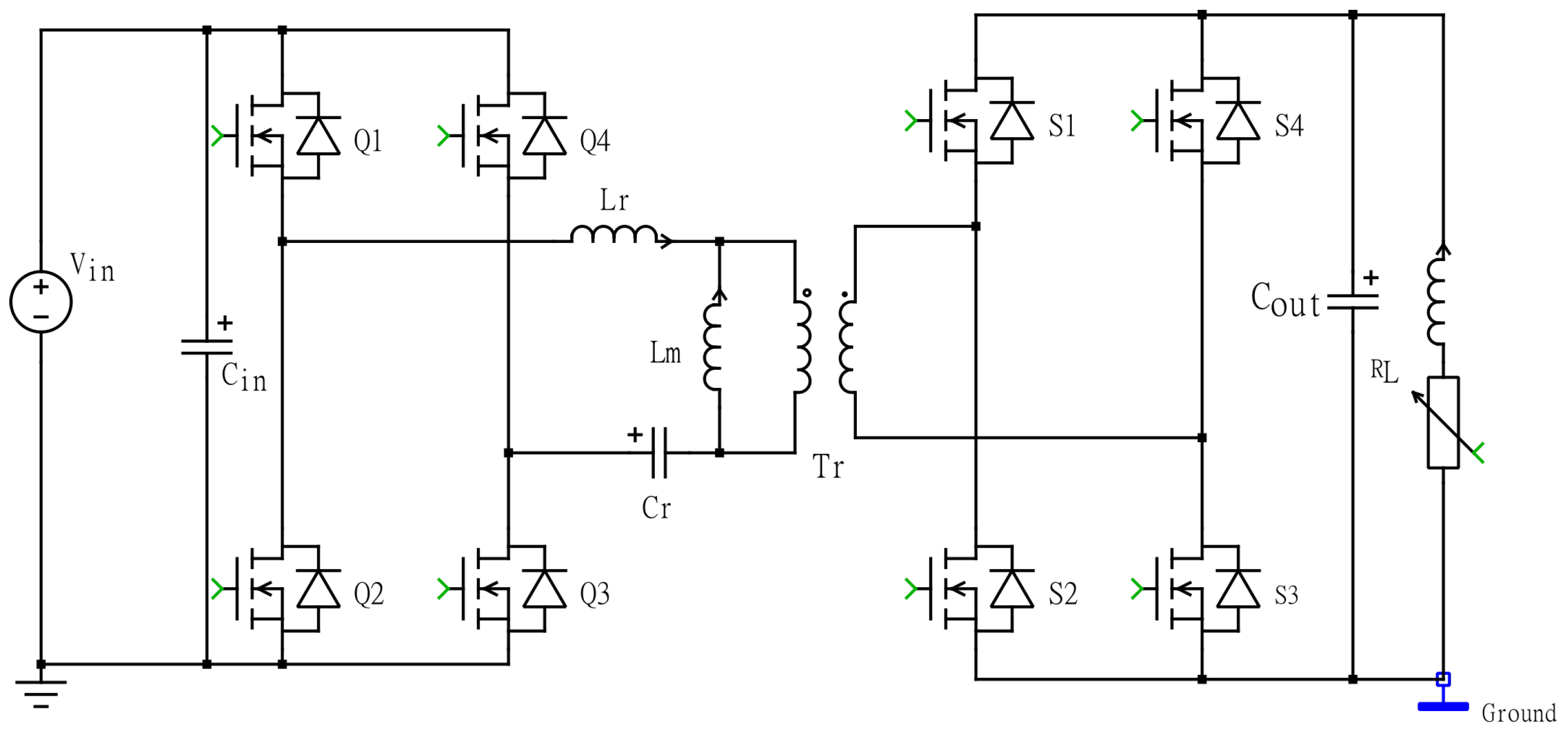
A resonant converter consists of a resonant network made of inductors and capacitors tuned to resonate at a specific switching frequency. The LLC converter consists of a series inductor, a shunt parallel inductor, and a series capacitor, which provide many desired advantages such as the regulation of the output voltage over a wide input voltage variation range and large load fluctuations and the ability to achieve zero-voltage switching (ZVS) over the complete operation area. Figure 2 shows a typical LLC converter circuit schematic. The converter consists of an H-bridge on the primary side and another rectification H-bridge on the secondary side. In order to produce a square-wave voltage waveform, the switches (Q1, Q3) and (Q2, Q4) are gated in a complementary fashion. The switches in question are operated at a fixed 50% duty cycle with an adjustable switching frequency (Fsw). To avoid cross-conduction, a short dead time is usually inserted during the turn-on and turn-off of the complementary switching pairs. The dead time provides a time window for the current to commutate to the body diode to achieve ZVS switching.
The rectification stage consists of full-bridge synchronous rectification FETs operated at the same switching frequency as the primary bridge. The resonant tank is comprised of the resonant capacitance (Cr), and two inductances—the series resonant inductance (Lr) and the transformer’s magnetizing inductance (Lm). When a square-wave voltage is applied to the LLC resonant network, the resonant network produces a sinusoidal current that is amplified or reduced by the transformer and converted to dc in the rectifier circuit. The output capacitor filters the rectified ac signal and outputs a dc voltage. As shown in Figure 2, three unique reactive components make up the resonant tank: Lr, Lm, and Cr. Consequently, the LLC circuits can be attributed to two separate resonance frequencies. The converter normally operates near the main resonance frequency (F0) formed by Lr and Cr (also known as inductive region) to achieve best efficiency. However, if the converter operates below the second resonance frequency F2 created by Lr, Lm, and Cr, the converter enters the capacitive region and the ZVS characteristics are lost. Based on the load condition (full load to partial load) LLC-converter can operate near, under, and beyond the F0 frequency and still achieve ZVS naturally. The converter can obtain gains equal, more, or less than unity based on the operation frequency. It is worth noting that the switching frequency determines the mode of operation. The determination of other key design parameters is discussed in Section 3.

2.2. Proposed Converter

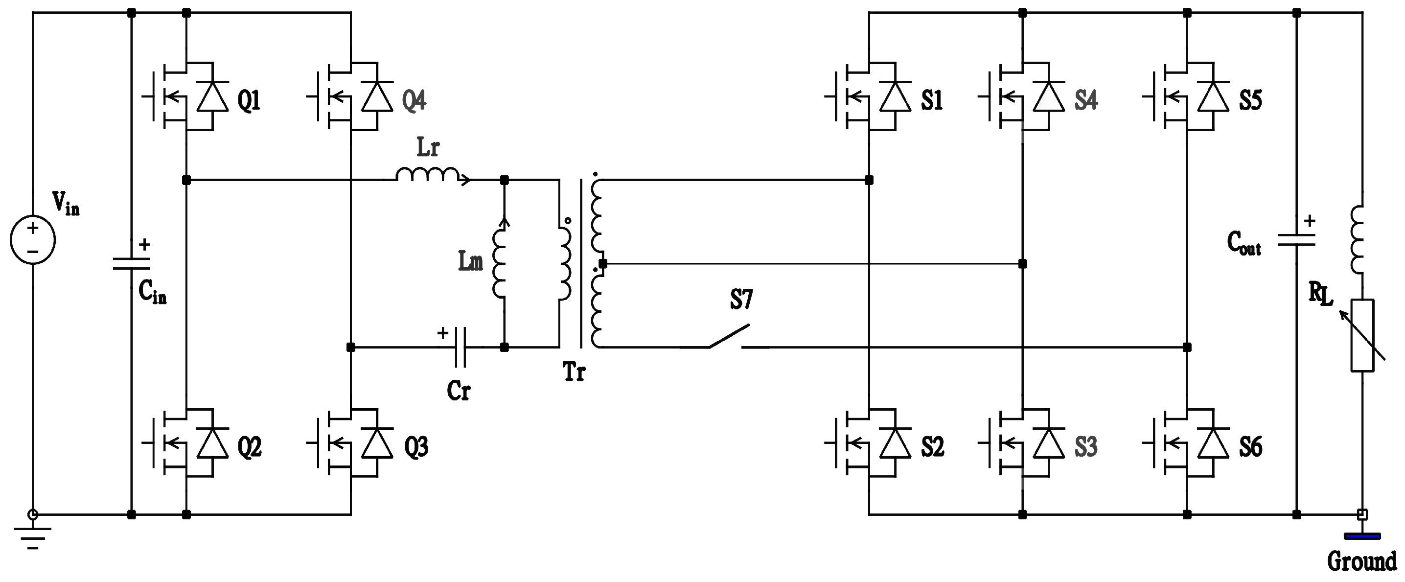
Under permanent failure conditions, SiC switches can go into one of two states: open circuit (OC) or short circuit (SC). Such failures, particularly in the SC situations, might lead to catastrophic destruction to the power source. The auxiliary converter must be switched off in such instances to protect the fuel cell, which will cause power loss in auxiliary components like sensors, and fans/blowers, which are dependent on the said converter’s power supply. When a failure is identified, the proposed converter uses the already failed switches to reconfigure the primary side of the converter to a half bridge (HB). While the converter enters this mode of operation, it should be able to supply limited power to the auxiliary loads without sacrificing its critical functionality. The proposed converter is depicted in Figure 3. The proposed converter has a structure identical to that of a full-bridge LLC converter, except that the secondary side has an extra branch made up of two MOSFETs (S5 and S6). This extra leg is energized when the switch S7 is continuously turned on. The switch S7 can be a semiconductor switch or a fast–acting relay. In addition, the transformer (Tr) has a secondary and tertiary winding with the same turns ratio with respect to the primary side. The three nodes of the transformer windings on the secondary side are connected to the switch nodes of bridges, respectively. In case of a fault, these additional components are utilized to create an active voltage doubler and regain the nominal output voltage and current. The detailed operation principle is described in the next section.

2.3. Operation under Fault

The reconfiguration of the converter is described by using a hypothesized potential fault situation. Here, the switch Q3 in Figure 3 is permanently damaged during operation by a SC fault. As a result, the faulty full bridge does not produce a symmetric waveform. To achieve fault tolerance, the following steps are taken:
  • To reconfigure the primary side of the converter to an HB, the switch Q4 is open–circuited permanently. Since Q3 is permanently short–circuited, the switch Q3 is henceforward assumed as a permanent short–circuited path and utilized as part of the current commutation path as a closed link.
  • The switches Q1 and Q2 are now gated with complimentary PWM control signals, which form the HB circuit. This can be observed by looking at the current paths of the primary side of the converter in Figure 4 and Figure 5.
  • Simultaneously, in the secondary bridge, the switch S7 is turned on continuously, and the bottom node of the transformer is connected to the middle node of the switch–pair S5, S6. Since the switches S4 and S3 are no longer part of the rectification circuit, they are deliberately left open–circuited by turning their respective gate signals off and are unused for the duration of this mode.
  • Since S5 and S6 are available in the secondary rectification path, S1, S6, and S5, S2 are switched in a complementary fashion to achieve a synchronous rectification. Note that by choosing this configuration, both the secondary and the tertiary windings of the transformer are energized.
Topologically, an HB can only produce half of the voltage of an FB configuration. Hence, if the secondary side had not been reconfigured, the voltage gain of the converter would be halved [28]. This difficulty is mitigated by the transformer employed in this converter. As in the reconfiguration mode, the transformer’s secondary and tertiary windings are both simultaneously energized, the effective turns ratio changes from n:1 to n:2 (where n is the turns ratio), effectively doubling the voltage of the half–bridge output. Since the effective turns ratio is halved, the voltage gain doubles, and the nominal output voltage is restored. The current path of the primary and secondary sides in the reconfigured settings during the positive and negative half of the cycle is shown in Figure 4 and Figure 5, respectively. The key switching diagrams for fault–free and under–fault operations are depicted in Figure 6. It is worth mentioning that the resonant inductor will experience double the root–mean–square (RMS) current with respect to the normal operation mode (inductor rating must be increased ), and the resonance capacitor will have double the voltage ripple with a dc offset (it requires capacitors with higher voltage ratings). In summary, in the occurrence of a SC/OC fault, the converter reconfigures itself to an HB configuration and the transformer with a modified turns ratio and, combined with a couple of new switches, doubles the voltage of the output of the rectification stage so that the output voltage at the load side remains the same.
The proposed converter can only withstand a fault in one of the switches on the primary side. If a failure is detected in the secondary side switches, the secondary can be also reconfigured as mentioned in [28]. However, this is not included in the scope of this paper and is not discussed.

2.4. Fault Detection Mechanism

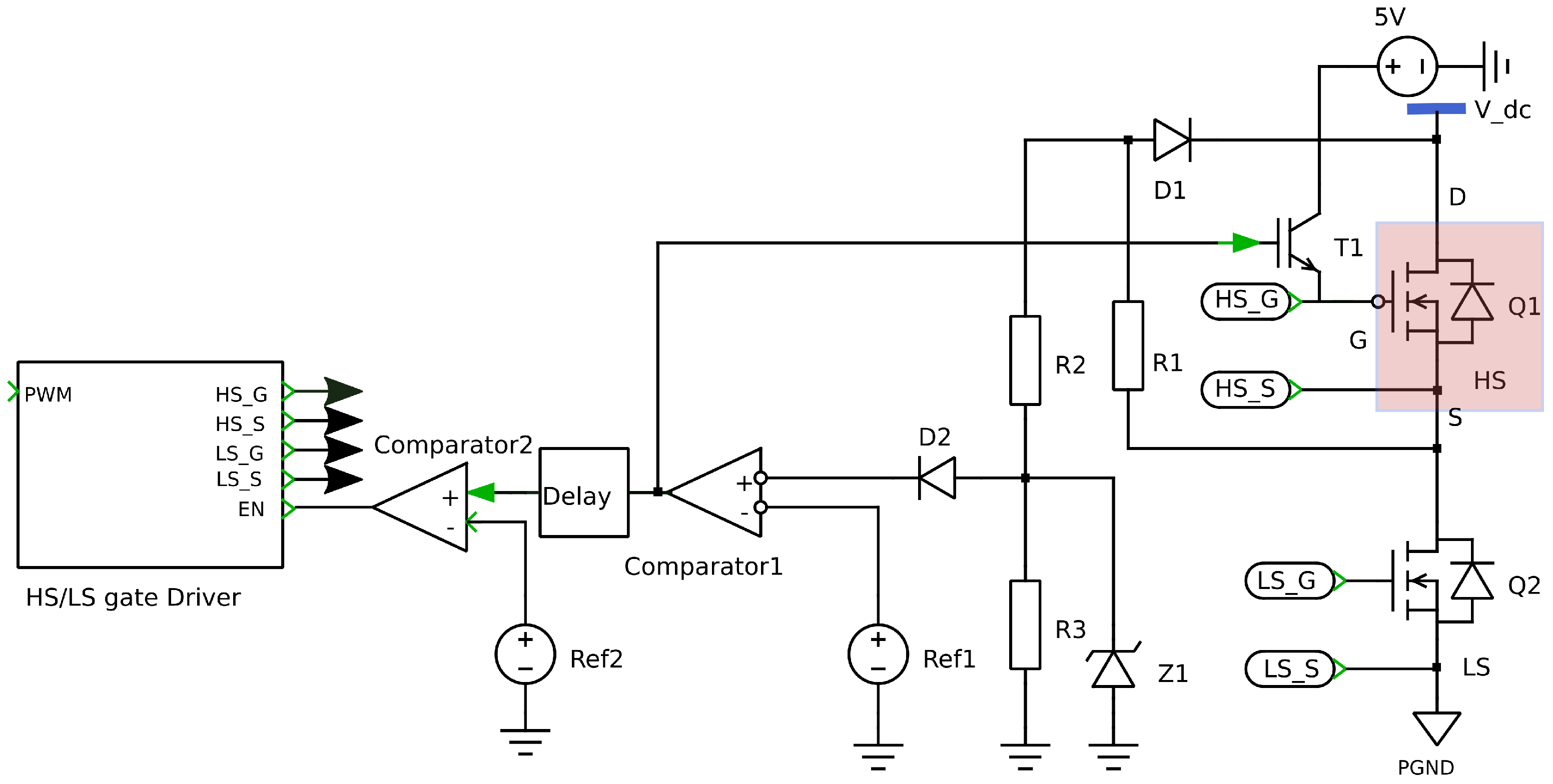
Since the SiC MOSFETs are particularly vulnerable to short circuit currents and typically exhibit limited SC withstand capability, the response time of the fault detection and protection circuit is highly critical. Several methods of fault detection have already been reported [29,30,31,32]. A possible method for detecting short circuits in SiC switches is shown in Figure 7. This method described below can be used to detect overcurrents and short-circuits in SiC switches in each of the H–legs (typically known as high-side (HS) and low-side (LS) switches), with a combination of HS–LS gate drivers [33]. SiC gate drivers normally provide a positive pulse (typically of 15–18 V) to turn on and a negative pulse (typically −3 V to −4.5 V) to turn off the switch. The proposed detection circuit needs access to the gate and source pin of the HS and LS MOSFETs, as well as an additional connection to the drain the pin of the MOSFETs. The fault-detection hardware works in the following way: during the occurrence of an overcurrent fault (OCS) on either of the switches (here only a fault in HS switch Q1 is considered), the current through the HS switch rises rapidly until saturation voltage is reached. Hence, reading the drain-source voltage (VDS) speedily becomes very critical. The high-voltage (HV) diode D1 between drain and source of switch Q1 becomes forward-biased when the gate driver attempts to turn on Q1. The resistance bridges R2 and R3 parallel to D1 sense this voltage drop (VDS + voltage drop across D1) and compare it (Comparator1) with the set reference voltage Ref1 to trigger the protection stage and send a fault flag to the onboard master controller. A similar circuitry can be employed on the low side to detect such faults as well. If the overcurrent fault persists for a predetermined number of cycles, the corresponding switch can be deemed as permanently failed (SC failure). The open-circuit (OC) detection is relatively simpler and can be done by monitoring each of the switching node voltage with respect to ground with a resistive voltage divider and monitoring the pulses with a controller. If the controller no longer detects a square pulse, a switch in the corresponding leg is faulty and has an overcurrent failure.
Beside the detection of large OCS or SC, it is also important to withdraw the gate signal to the affected switch efficiently, in order to try to save it. However, if a SiC MOSFET is turned off hard while it is carrying a high amount of drain current, it will introduce considerable VDS ringing across the switch. In some cases, they can exceed the absolute value of the VDS and may irreversibly damage the switch. Hence, a two-level turn-off system where the gate voltage is pulled down to a lower value first and afterwards pulled down to a negative value provides an excellent way to mitigate the ringing problem [33]. The circuit explained above can be further adapted to implement a two-level turn-off system. In order to achieve a two-level turn-off, the output signal of the comparator is used to bias the base of switch T1. This in turn, ties Vgs to the 5 V source. After a predefined delay, Comparator2 is triggered, and it signals the gate driver (typically through the EN pin) to withdraw the gate signal. Vgs is hence tied to the −3 V, and the affected switch is finally turned off.

3. Converter Design

3.1. Resonant Stage Design

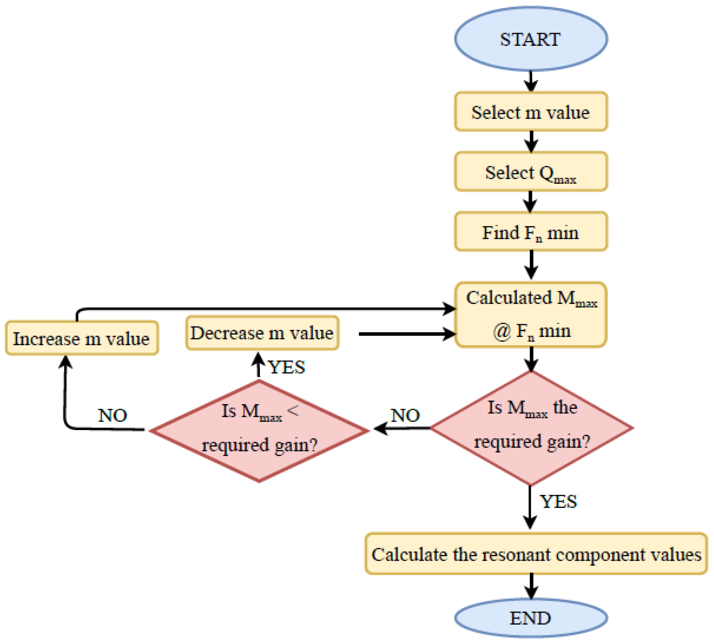
The design of full-bridge resonance converters for different power levels is described in [34,35]. The main design parameters are F0 (resonance frequency), m (magnetization ratio), n (transformer turns ratio), and Qmax (quality factor). However, the design of key design parameters is an iterative process and must be checked against the physical and operational constraints of the converter. The suggested optimization process is shown in Figure 8.
In this section, the design steps to derive the resonant parameters are described in brief:
  • The first step is to obtain the turns ratio of the transformer. The turns ratio of the transformer depends on the nominal input voltage (Vin,nom), output voltage (Vo), forward MOSFET voltage drop (VDS,on), and the diode forward voltage drop (Vf) and can be obtained from Equation (1).
    n eq = V in , nom 2 × V DS , on V o + 2 × V f
  • Alongside, the maximum voltage gain (Mmax) and minimum voltage gain (Mmin) are to be determined. The voltage gain is the ratio of output voltage and input voltage, and is not a fixed value, if the input voltage of the converter fluctuates. These two parameters are calculated based on design constraints based on Equation (2):
    M max = V in , max V in , nom M min = V in , min V in , nom
    In order to deal with overload capacities of the converter, a safety factor of 1.2 is considered.
  • The transformer inductance ratio (m) = (Lm + Lr)/Lr is another important parameter for the design. It is defined by the ratio of the primary magnetization inductance (Lm) and the equivalent leakage inductance (Lr). The transformer inductance ratio (m) is an important parameter that helps shape the gain curve. By selecting a smaller values of m, a higher voltage gain can be achieved with a narrow range of frequency modulation. Hence, lower values of m are more suitable for a wide input voltage range. On the other hand, choosing a small value of m means a very large Lr and a small value of Lm resulting in a very poor transformer coupling and thereby, reducing the efficiency due to a large circulating current [34]. A higher value of m increases the efficiency at the cost of a reduced voltage gain and a narrow range of frequency modulation. Therefore, the value of m is generally set between 3 and 7. An iterative method is normally employed to choose the optimal value of m based on input design parameters.
  • The voltage gain after the integration of the transformer leakage differs from the voltage gain derived in Equation (3) by a multiple of Mv. This is the fixed gain at resonant frequency and it is given by:
    M v = m m 1
    Without the integration of the transformer leakage inductance, the gain in Equation (3) is unity [36]. Therefore, the equivalent turns ratio after the inclusion of the transformer leakage inductance is given by:
    n = n eq M v
  • The final step is to obtain the converter transfer function to attain the gain curve of the system. The time-domain analysis of an LLC converter is a very cumbersome process as the presence of nonlinear reactive elements in the converter and hence the resulting transfer function is typically nonlinear. To simplify the design procedure, first harmonic approximation (FHA) method is often employed. In this methodology, only the first harmonic signals are thought to contribute to power transfer. As a result, all current and voltage waveforms are presumed to be sinusoidal in nature. The FHA also helps determining the necessary constraints for the primary bridge to achieve ZVS. The transfer function H ( j ω ), also known as the voltage-gain function (i.e., ratio of output to input voltage) is shown in Equation (5).
    H ( j ω ) = 1 n · R ac | | j ω L m 1 j ω C r + j ω L r + R ac | | j ω L m
    The real part of Equation (5) can be represented as:
    H ( Q , F n , m ) = F n 2 · ( m 1 ) ( m · F n 2 1 ) 2 + F n 2 · ( F n 2 1 ) 2 · ( m 1 ) 2 · Q
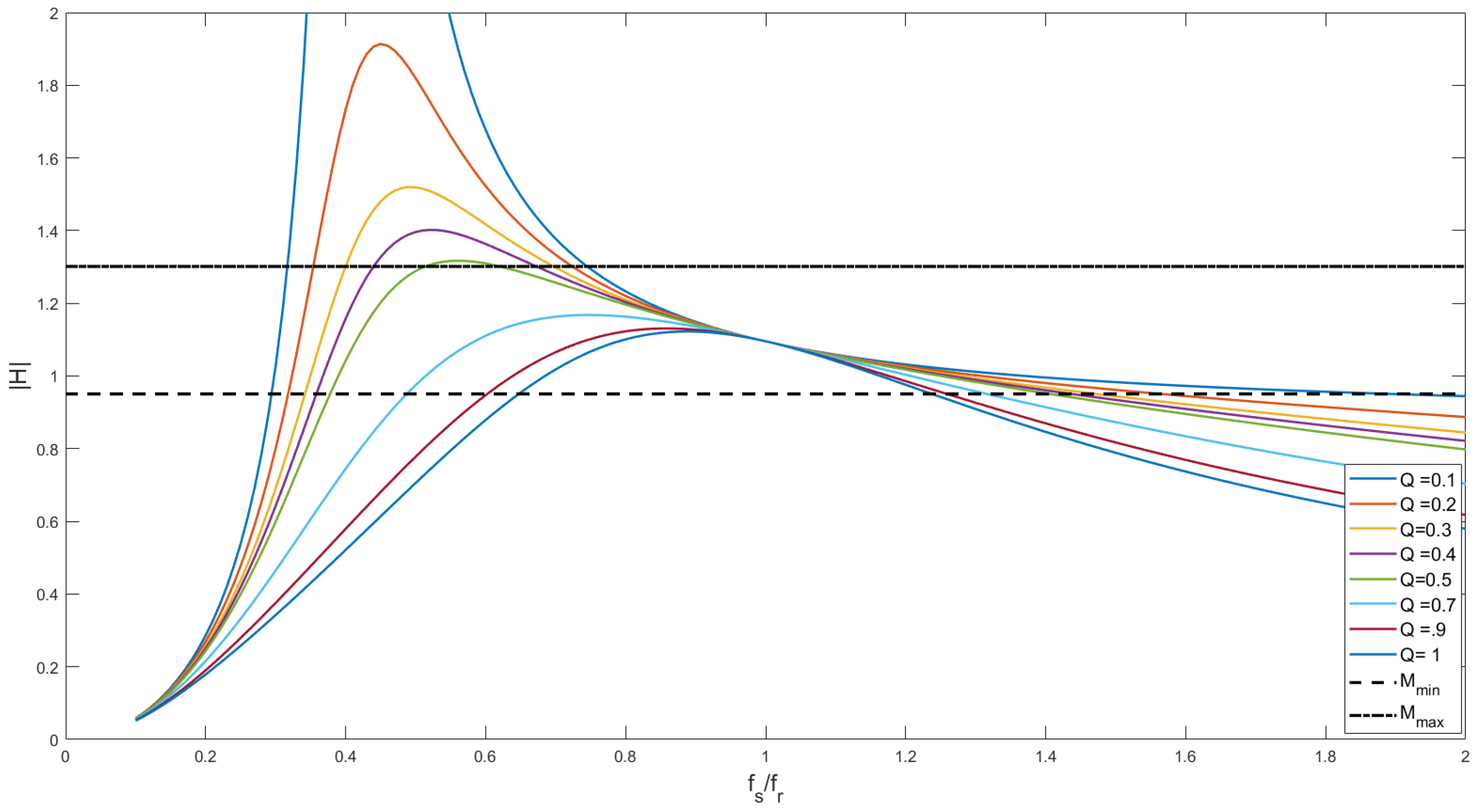
    Plotting the gain vs. the normalized switching frequency with respect to the variable Q values gives an idea of which value of Qmax would satisfy the gain requirement. From Figure 9 it is evident that for m = 6 a Qmax = 0.45 would suffice.
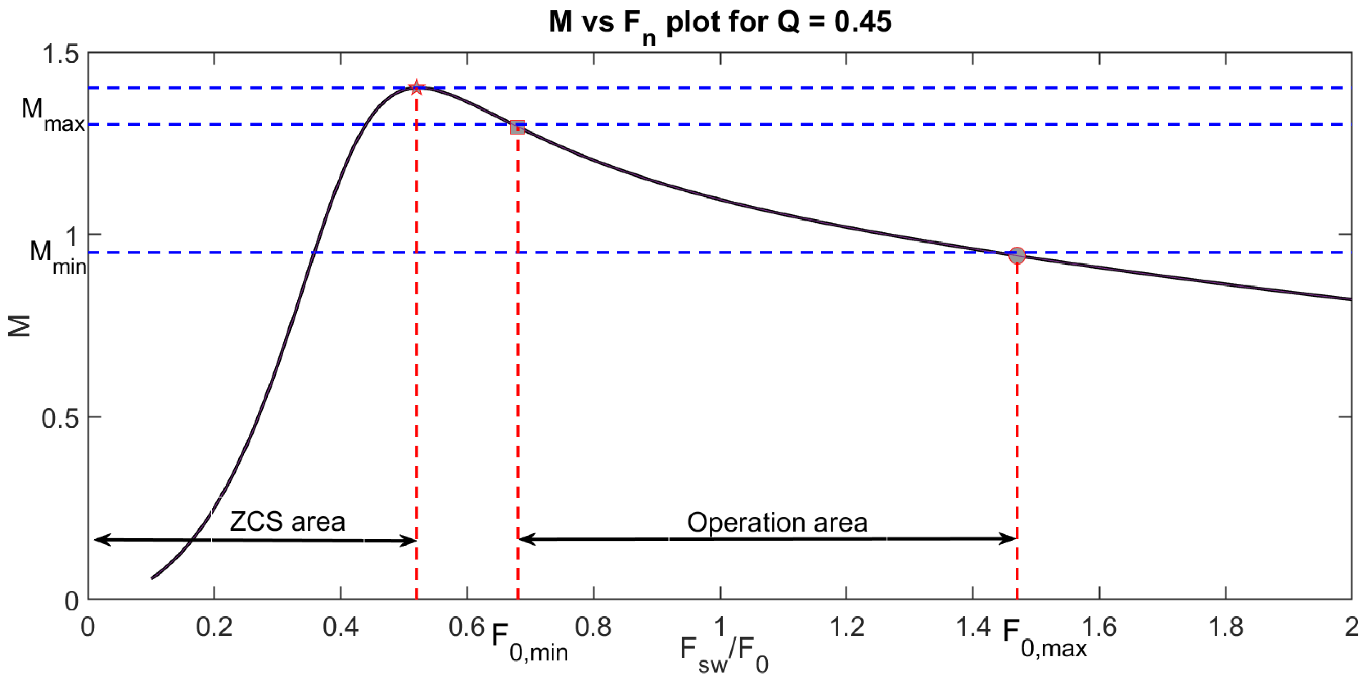
    The gain curve is plotted again with the selected value of Qmax = 0.45 and m = 6 and shown in Figure 10. From the intersection of the maximum and minimum gain values, the frequency limit of inductive ZVS operation can be determined. The switching frequency must never go below the frequency where the peak occurs (as the converter enters a capacitive mode and it is not recommended).
  • Finally the resonant tank parameters can be calculated from the following equations:
    F 0 = 1 2 π L r C r Q max = 1 R ac · L r C r R ac = 8 π 2 V o I o = 8 π 2 R 0
The designed resonant tank parameters based on the input parameters using the optimization technique described above are tabulated in Table 1.

3.2. Secondary Stage Design

The secondary side of the converter design is critical due to the fact that it must be able to handle and safely rectify a high amount of current. In traditional rectifiers, the rectification is done by diodes in half– or full–bridge configuration. As the converter in hand deals with a large amount of current, a full–bridge rectification stage was considered. However, the diodes in the rectification stage would be particularly problematic because the high forward voltage drop and high on–state resistance would cause huge conduction losses (considering static and dynamic losses) and ultimately result in poor converter efficiency. Although parallel SiC diodes would decrease the dynamic losses to a certain extent, it would not affect the static losses. The conduction loss equation for a diode is given by the following equation:
P Diode = V forward × I Diode , avg + R Diode × I Diode , rms 2
Alternatively, instead of the diodes SiC MOSFETs can be used (with very low Ron) and can be operated in synchronous rectification (SR) mode. The conduction loss equation of the synchronous rectifier MOSFET is given by:
P cond , MOS = R DS , on × I Diode , rms 2
A comparison of the conduction losses (based on LTSPLICE model data) between a SiC–based high–current diode GC2X15MPS12–247 [37] and a SiC–based MOSFET C3M0015065K [38], with respect to current and junction temperature was carried out and is shown in Figure 11. The analysis attest to the fact that for high current applications, the MOSFETs are clearly the superior candidate with respect to conduction losses during continuous rectification operation.
When MOSFETs are used in FB SR configuration, a special controller must be used to use the MOSFETs as diodes. The principle of doing so is the following: when the body diode of the MOSFET starts conducting, the corresponding SR detects the positive anode–cathode voltage and fires the main switch, causing the current to commute from the diode over to the main switch. As a result, the body diode conducts for around 2% of the total conduction time, and during the rest of the forward conduction time, the current flows through the main switch. Due to the superior on–state resistance, the conduction losses, as well as the cooling requirements can be significantly reduced. It is worth mentioning that no commercially available single SiC MOSFETs are capable of carrying such a high current, and hence paralleling several MOSFETs is recommended.

4. Control System

The control system of the power converter ensures the desired behavior of the system and increases its stability. The proposed converter in normal operation mode performs just like the conventional LLC converter. Hence, standard control strategies that employ a voltage–controlled oscillator (VCO) to generate a frequency–modulated PWM can be used [39]. In order to simplify the digital control system design process, the control–to–output transfer can be obtained from a simulated small–signal analysis. The principle of a small–signal analysis is simple: in a converter operating in open–loop mode, a very small sinusoidal perturbation (which does not affect the converter operation) with a variable frequency range is added, and the impact of the injected perturbation on the output variable is derived. The frequency analysis obtained (bode plot) can be further used to derive an approximated transfer function of the plant. The transfer function derived can be further used to derive the PI–based digital controller to establish a closed–loop system.

4.1. Gain Parameter Look–Up Table

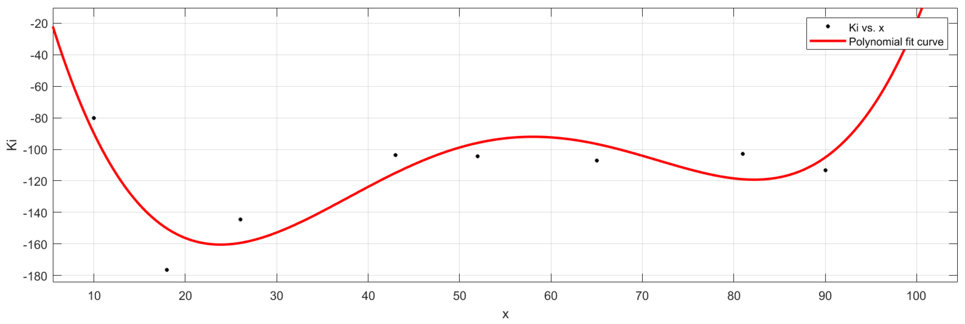
The traditional PI–controllers for LLC converters often suffer from the problem of poor regulation abilities with respect to wide input variations and sudden load changes. The problem lies within the fact that a controller with fixed gain parameters is often unsuitable to tackle such disturbances. In order to deal with this problem, a variable gain controller can be used. In order to obtain appropriate gain values for different per unit (p.u) load values, a small–signal analysis was carried out with different load conditions, and suitable gain parameters were derived using a PI–controller tuner to achieve the best regulation, at least 20 dB gain–margin, more than 60 deg phase–margin, and the same settling time for each case. From the analysis, it was evident that the parameter Kp could be left unchanged, but the parameter Ki had to be changed when the load changed. Finally, these values were plotted, and using a curve fitting tool, the best possible curve equation was obtained. To demonstrate the technique, for a given converter parameters Ki for the given converter were obtained and plotted as shown in Figure 12, and the fitted–equation is shown in Equation (10).
K i ( x ) = p 1 x 4 + p 2 x 3 + p 3 x 2 + p 4 x + p 5
where (Coefficients with 95% confidence bounds),
p1 = 59.85 (30.97, 88.73)
p2 = −1.428 (−22.85, 20)
p3 = −107.9 (−173.3, −42.42)
p4 = 25.83 (−10.64, 62.3)
p5 = −93.41 (−118.8, −67.97)
This equation can be easily used as a look–up table and can be used to determine an appropriate gain value for different p.u load values.

4.2. Control Strategy

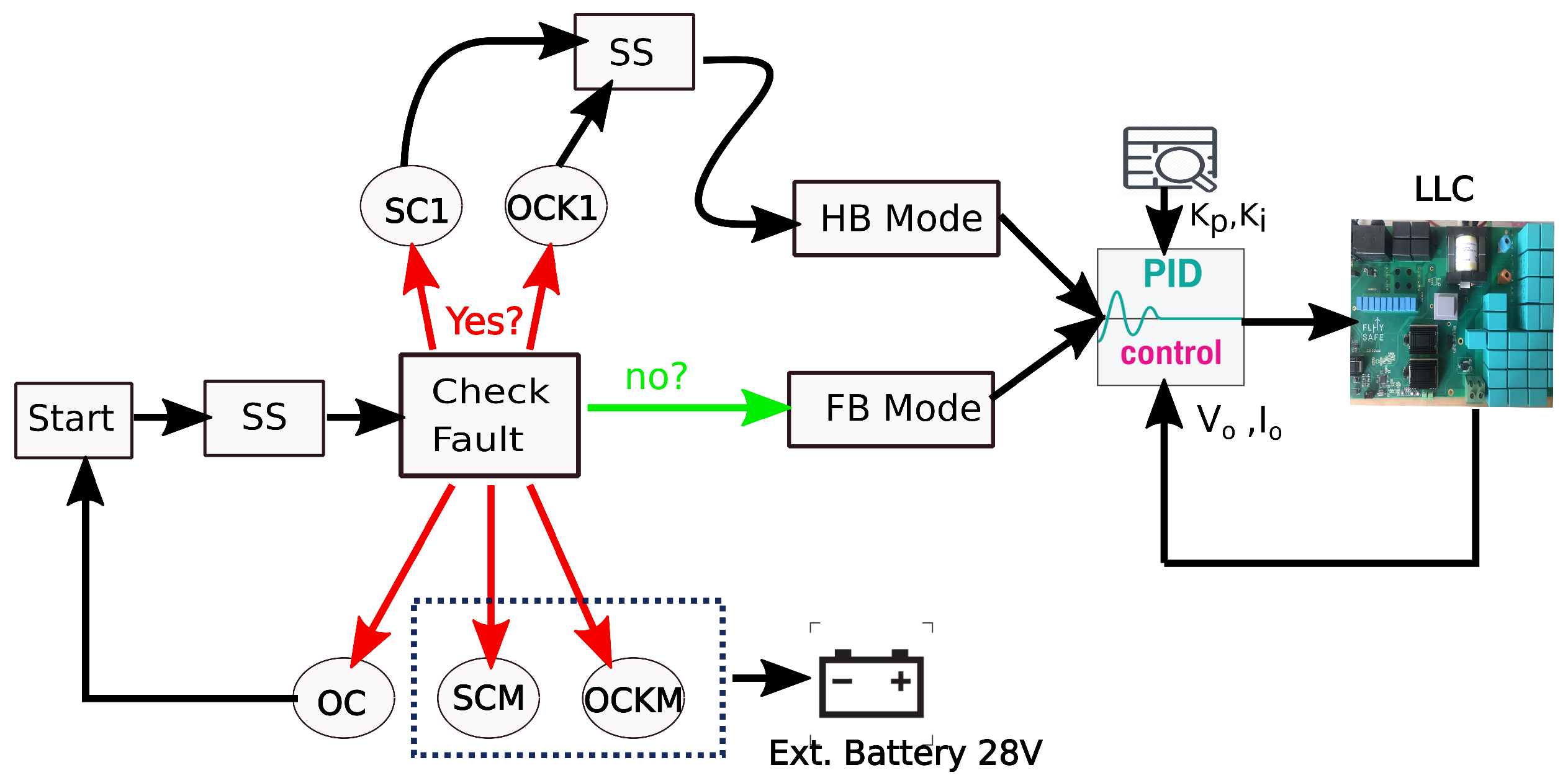
The control algorithm of the proposed converter is shown in Figure 13. Upon initiation of the starting sequence, the converter is powered on with a soft start. Following the start up, a parallel diagnosis state is initiated, which always interacts with the fault–detection circuitry to check for faults in the switches. If there is no fault in the system, the controller enters FB mode, and a look–up table–based PI controller (based on the output voltage and p.u load) generates the PWM signals to drive the LLC converter. In case of a fault, the controller enters one of the following states: overcurrent (OC), short circuit in one switch (SC1), short circuit in multiple switches (SCM), open circuit in one switch (OCK1) or open circuit in multiple switches (OCKM). Upon detection of any of the fault states, the controller shuts down the gate signals and reinitiates the soft–start (SS) sequence to check if the fault persists. If the fault still remains, based on the fault state, the following steps are taken:
  • In case of OC, the load current is limited and it is checked if the fault is cleared. Otherwise, the state is changed to SC1 or SCM based on the number of switches affected.
  • In case of SCM or OCKM, the converter is unusable and the auxiliary battery must be engaged.
  • In case of SC1, the converter enters the HB reconfiguration mode and decides which switches must be used to achieve HB operation based on the logic Table 2. Similar logic can be derived for the OCK1 state.
  • The transition from FB mode to HB mode is accompanied with an SS sequence, in order to reduce the output voltage overshoot caused by the sudden inductive current step.

5. Experimental Results and Discussion

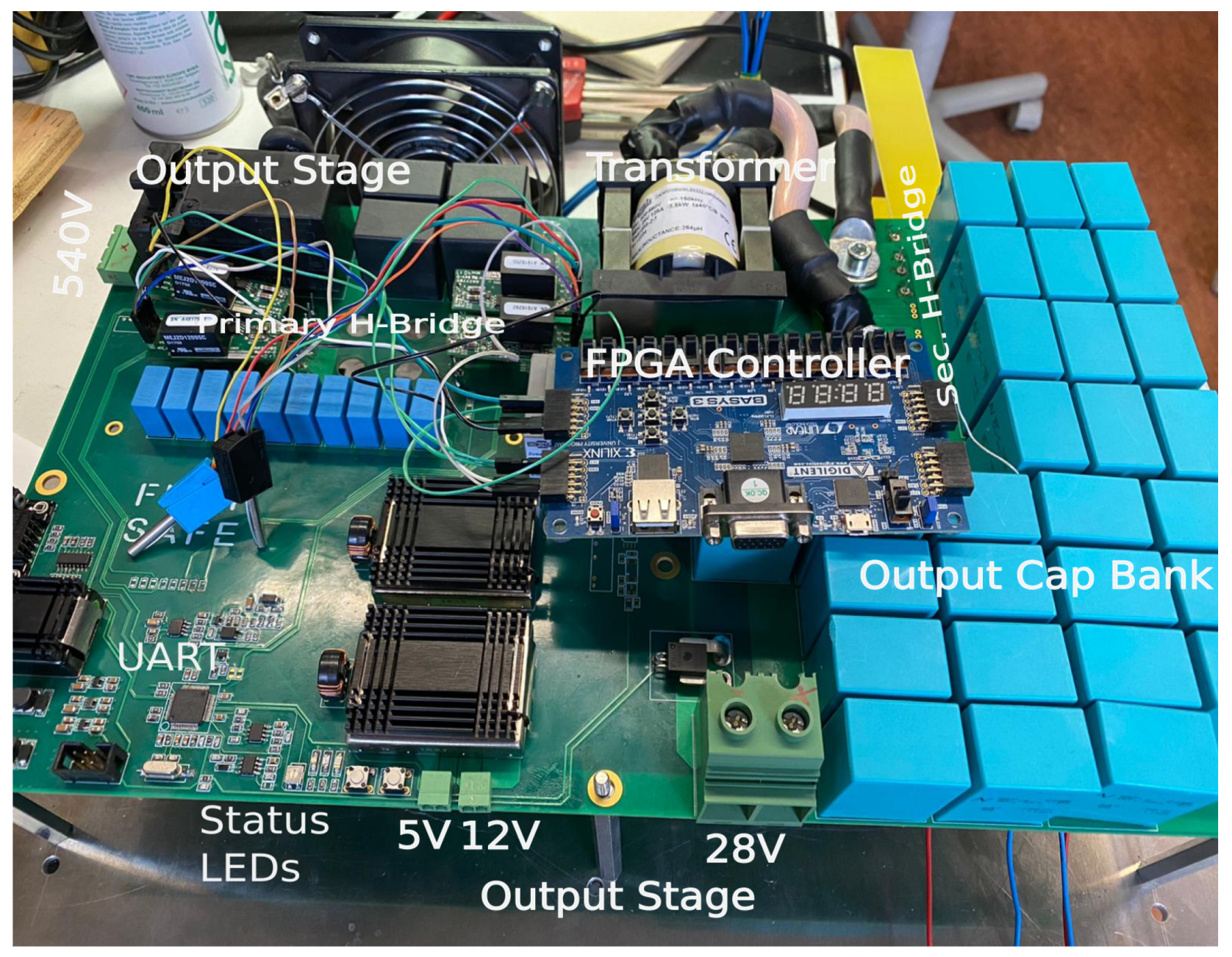
In order to verify the concept and design of the proposed reconfigurable LLC converter, a 2.0 kW converter prototype was built, and experimental results were recorded. This converter was specially modified to conform to popular aircraft and EMI standards. Figure 14 shows a photo of the converter. The input parameters (based on MIL–STD–704) and the resonant tank parameters are listed in Table 1. The converter also featured a precharging circuit for the input capacitors and auxiliary 5 V and 12 V outputs alongside the main 28 V output. These extra power outputs can be directly accessed by different sensors and meters inside the aircraft. The primary side H–bridge consisted of C3M0015065K–based SiC MOSFETs (with a Kelvin connection), which can block up to 650 V and exhibit a very low RDS,on. The secondary side synchronous rectifier consisted of 16 CSD18532KCS [40] MOSFETs (four per leg) and these MOSFETs were controlled by an LM74670–Q1–based [41] dedicated controllers. To ensure clean switching of the primary–side SiC MOSFETs and to avoid cross–talk, CGD15SG00D2 [42] gate drivers were used to drive them. The switch S7 was recreated by using two high–current IGBTs connected in an opposite back–to–back series fashion (capable of blocking current in both directions when turned off). The output capacitor bank consisted of multiple polypropylene film capacitors to deal with very high current ripple requirements. The control algorithm was implemented with an Artix–7–based FPGA board [43], with additional controllable user action buttons and frequency/output voltage/fault display. The look–up–table–based digital PI controller (two–pole and two–zero based) was implemented onto the FPGA. The converter always operated in a closed–loop under all conditions. The embedded code was generated using the Embedded Coder Support Package for the Xilinx Zynq Platform for Matlab 2019a version [36].
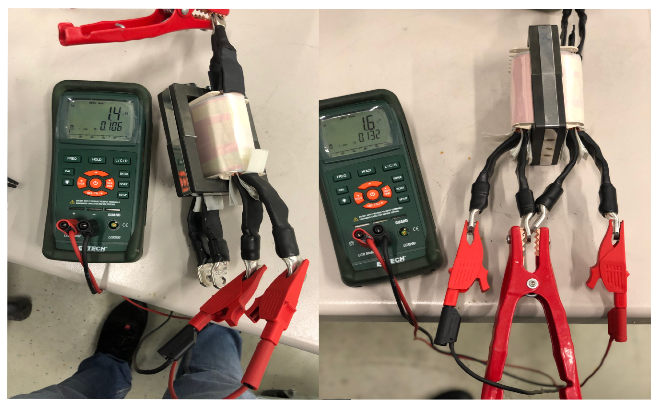
The transformer used to achieve fault–tolerance is shown in Figure 15. The transformer was designed with an E–E core (EE100/27.5) and made from SIFERRIT N87 material. The transformer had copper–foil–based secondary and tertiary windings. The windings were arranged in a double–helical winding arrangement. The leakage inductance was achieved with an air gap of 0.75 mm. The measurement of leakage inductance revealed no significant change in leakage inductance when only one or both windings were engaged. Hence, irrespective of whether only the secondary winding or both the primary and the secondary windings were energized, the LLC converter transfer function remained unchanged, and no modification of the control algorithm was necessary.
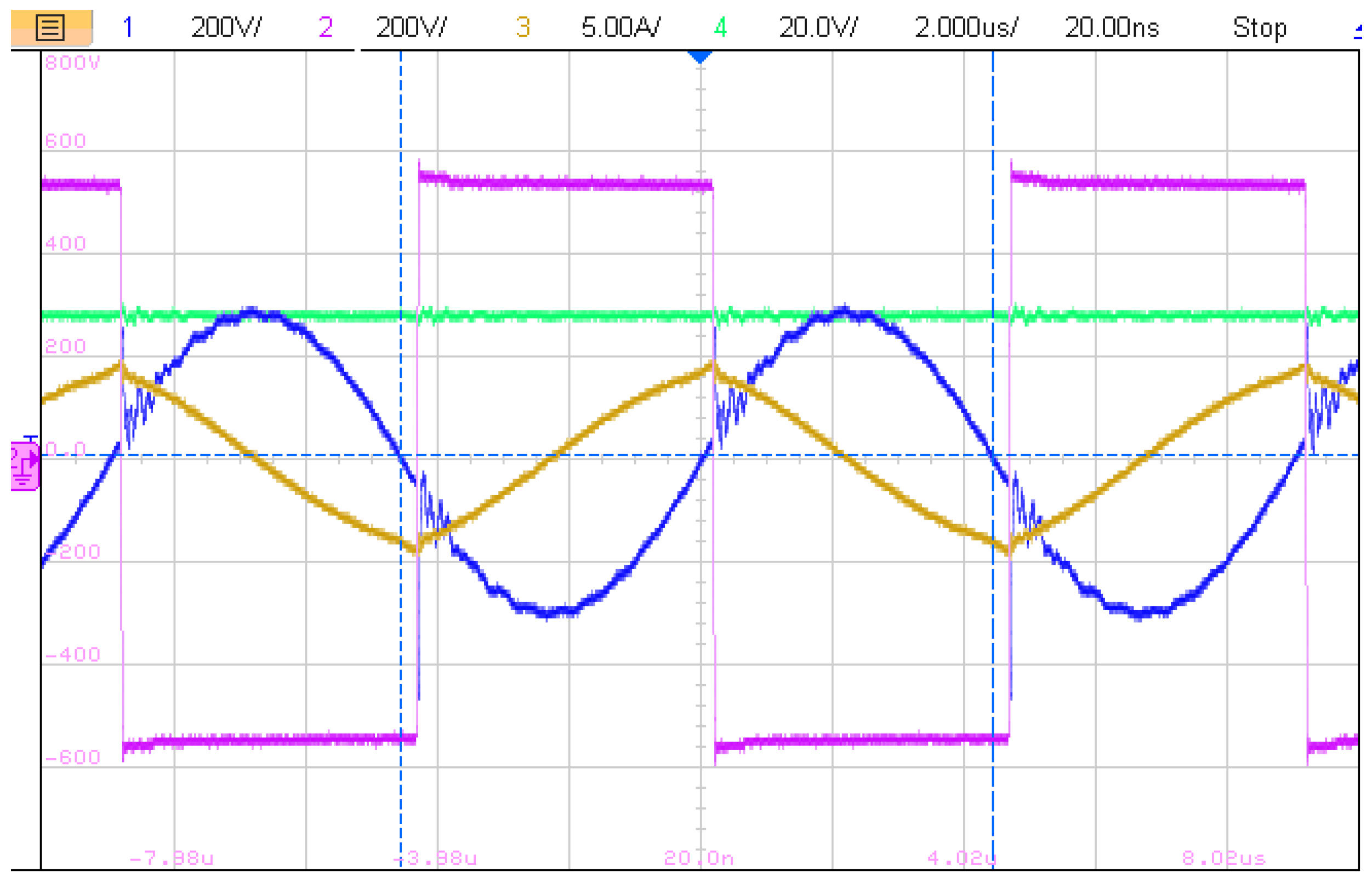
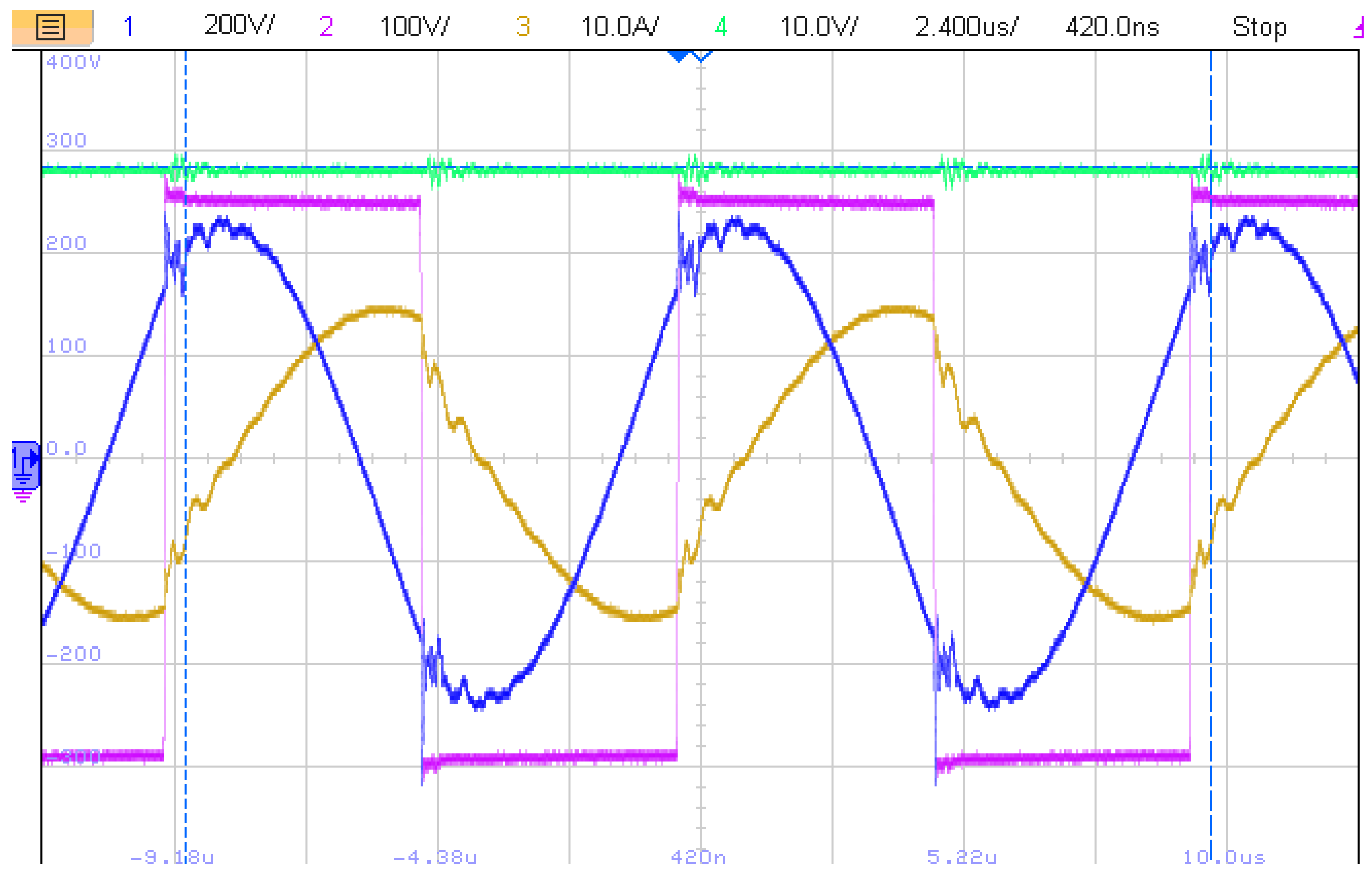
Initially, the converter was tested for normal operating conditions at full load, where it was excited by a 540 V dc supply and the primary side transformer voltage (Vpri), resonant capacitor voltage (VCr), output voltage (Vo) and inductor current (Ir) waveforms were observed under full load condition. As seen in Figure 16, a 100 kHz square wave switching from +540 V to −540 V is impressed upon the primary side of the transformer, and as a result, the secondary side produces a scaled–down square wave of the same frequency (not shown), and a dc output voltage (o) of +28 V is obtained after the rectification stage. The inductor current is also shown, which has an RMS value of around 4.8 A. It can be seen that near resonance frequency, the ZVS is achieved, which attests to the theoretical analysis.
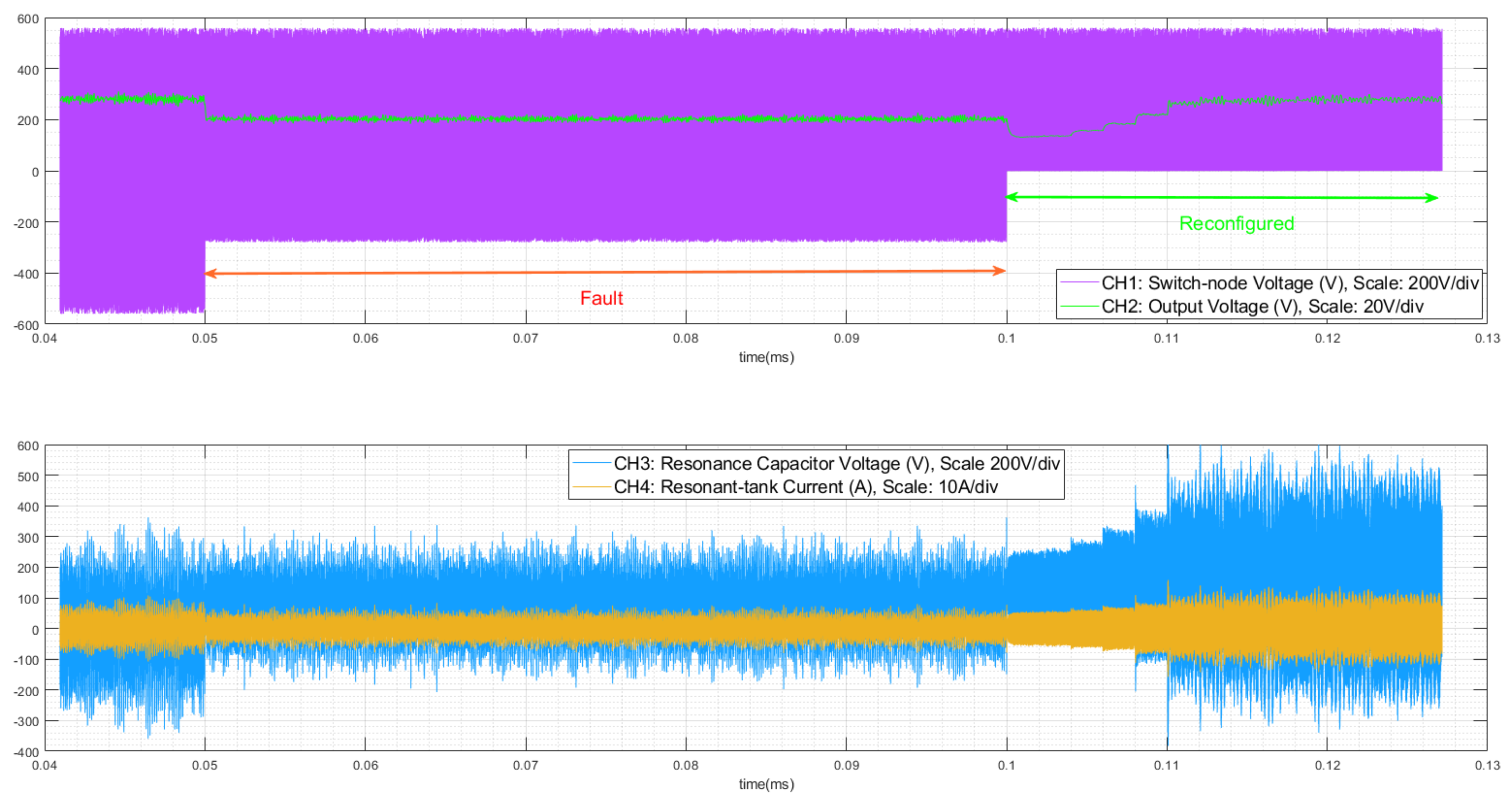
Finally, the reconfiguration circuit concept was evaluated. A test profile was loaded onto the FPGA and the results imported from the data logger of the oscilloscope are shown in Figure 17. The converter was first powered on to artificially evaluate the fault scenario until it reached the nominal 28 V steady stage. Afterward, switch Q3 was forcefully short–circuited by the controller. As a result, the voltage dipped to around 14 V and stayed there until the detection circuit confirmed the fault diagnosis. The fault situation can also be ascertained from looking at the voltage waveform at the switch node, which no longer produced a symmetric ±540 V waveform. Next, the primary side circuit was reconfigured to an HB, and the secondary side transformer enable switch (S7) was activated, along with a soft start, and as can be seen in Figure 17 the output voltage recovered without sharp overshoots. The current stress on the resonant inductor and the voltage stress on the resonance capacitor was increased when the converter operated in this mode.
The converter waveforms after the fault are shown in Figure 18. As can be seen in the figure, the voltage across the transformer is now ±250 V, which is half of the magnitude compared to that in Figure 16. This is typical for an HB topology. However, due to the activation of both transformer windings, the voltage gain is doubled, and the nominal output voltage is regained. The resonant tank current and the capacitor voltage almost doubled while maintaining the sinusoidal form, and the ZVS characteristics are still retained.
The converter’s efficiency under various load conditions for normal and fault conditions was measured and is shown in Figure 19. The efficiency of the experiments ranges from 90.5 percent to 95 percent during normal operation. Several measurements were carried out to observe the input voltage variation in the range of 500–560 V. Low load conditions on the converter resulted in a lower efficiency since the converter had to switch at a very high frequency to achieve the necessary gain. The fault–mode measurements revealed a drop of efficiency of around 1.5% for high–load conditions. These additional losses can be attributed to the conduction losses in the S7 switch and heavier conduction losses on the primary side due to higher currents.

6. Conclusions

This paper presented a novel fault–tolerant resonant converter concept for high–current low–voltage applications. The mode of operation and reconfiguration strategy was discussed in detail. The converter design steps, fault detection technique, and a look–up–table–based dynamic control strategy were presented. Finally, a 2.0 kW SiC–MOSFETs–based converter was designed with the aid of the aforementioned concepts and experimental results were obtained. The experimental results proved that the converter regained the output voltage under fault and a soft start eliminated any voltage surges during the reconfiguration process. The proposed converter is ideally suited for future full–electric aircraft, where permanent power loss can be avoided in the case of failure in power electronics switches and the need for a bulky external backup battery can be eliminated.

Author Contributions

Conceptualization, S.B.; funding acquisition, J.K.; investigation, S.B.; methodology, S.B.; project administration, C.W. and S.B.; supervision, J.K. and C.W.; validation, S.B.; visualization, S.B.; writing—original draft, S.B.; writing—review and editing, C.W. All authors have read and agreed to the published version of the manuscript.

Funding

This project has received funding from the Fuel Cell and Hydrogen 2 Joint Undertaking under the European Union’s Horizon 2020 research and innovation programme under grant agreement No. 779576. This Joint Undertaking receives support from the European Union’s Horizon 2020 research and innovation programme and Hydrogen Europe and Hydrogen Europe Research.

Institutional Review Board Statement

Not applicable.

Informed Consent Statement

Not applicable.

Data Availability Statement

Not applicable.

Acknowledgments

The authors would like to thank our laboratory assistant Fatih Türk for the technical support during soldering and experiments.

Conflicts of Interest

The authors declare no conflict of interest.

References

  1. Rosero, J.A.; Ortega, J.A.; Aldabas, E.; Romeral, L. Moving towards a more electric aircraft. IEEE Trans. Aerosp. Electron. Mag. 2007, 22, 3–9. [Google Scholar] [CrossRef] [Green Version]
  2. Revol, B.; Azzopardi, S.; Youssef, T.; Teu, J.S.N.; Gautier, C.; Khazaka, R.; Roggia, S. Overview and new trends in technology bricks for reliability enhancement in future wide band gap power converters for More Electrical Aircraft (MEA) and More Electrical Propulsion (MEP) systems. In Proceedings of the IECON 2019—45th Annual Conference of the IEEE Industrial Electronics Society, Lisbon, Portugal, 14–17 October 2019; pp. 7128–7134. [Google Scholar]
  3. Nawawi, A.; Tong, C.F.; Liu, Y.; Sakanova, A.; Yin, S.; Liu, Y.; Men, K.; See, K.Y.; Tseng, K.J.; Simanjorang, R.; et al. Design of high power density converter for aircraft applications. In Proceedings of the 2015 International Conference on Electrical Systems for Aircraft, Railway, Ship Propulsion and Road Vehicles (ESARS), Aachen, Germany, 3–5 March 2015; pp. 1–6. [Google Scholar]
  4. Swaminathan, N.; Cao, Y. An Overview of High-Conversion High-Voltage DC–DC Converters for Electrified Aviation Power Distribution System. IEEE Trans. Transp. Electrif. 2020, 6, 1740–1754. [Google Scholar] [CrossRef]
  5. Clements, R.; Jones, R.W. DC-DC convertor design for the 270 volts DC ‘More Electric Aircraft’. In Proceedings of the 2018 13th IEEE Conference on Industrial Electronics and Applications (ICIEA), Wuhan, China, 31 May–2 June 2018; pp. 1847–1852. [Google Scholar]
  6. Mastromauro, R.A.; Pugliese, S.; Stasi, S. An advanced active rectifier based on the single–star bridge cells modular multilevel cascade converter for more–electric–aircrafts applications. In Proceedings of the 2015 International Conference on Electrical Systems for Aircraft, Railway, Ship Propulsion and Road Vehicles (ESARS), Aachen, Germany, 3–5 March 2015; pp. 1–6. [Google Scholar]
  7. Hoenicke, P.; Ghosh, D.; Muhandes, A.; Bhattacharya, S.; Bauer, C.; Kallo, J.; Willich, C. Power management control and delivery module for a hybrid electric aircraft using fuel cell and battery. Energy Convers. Manag. 2021, 244, 114445. [Google Scholar] [CrossRef]
  8. Shi, B.; Zhou, B.; Hu, D. A novel dual–output indirect matrix converter for more electric aircraft. In Proceedings of the IECON 2017–43rd Annual Conference of the IEEE Industrial Electronics Society, Beijing, China, 29 October–1 November 2017; pp. 4083–4087. [Google Scholar]
  9. Raghavendra, K.V.G.; Zeb, K.; Muthusamy, A.; Krishna, T.N.V.; Kumar, S.V.S.V.P.; Kim, D.-H.; Kim, M.-S.; Cho, H.-G.; Kim, H.-J. A Comprehensive Review of DC–DC Converter Topologies and Modulation Strategies with Recent Advances in Solar Photovoltaic Systems. Electronics 2020, 9, 31. [Google Scholar] [CrossRef] [Green Version]
  10. Krishna, T.N.V.; Sathishkumar, P.; Himasree, P.; Punnoose, D.; Raghavendra, K.V.G.; Himanshu; Naresh, B.; Rana, R.A.; Kim, H.-J. 4T Analog MOS Control–High Voltage High Frequency (HVHF) Plasma Switching Power Supply for Water Purification in Industrial Applications. Electronics 2018, 7, 245. [Google Scholar] [CrossRef] [Green Version]
  11. Pugliese, S.; Mastromauro, R.A.; Stasi, S. 270 V/28 V wide bandgap device–based DAB converter for more–electric–aircrafts: Feasibility and optimization. In Proceedings of the 2016 International Conference on Electrical Systems for Aircraft, Railway, Ship Propulsion and Road Vehicles amd International Transportation Electrification Conference (ESARS–ITEC), Toulouse, France, 2–4 November 2016; pp. 1–6. [Google Scholar]
  12. Buticchi, G.; Costa, L.; Liserre, M. Improving System Efficiency for the More Electric Aircraft. IEEE Ind. Electron. Mag. 2017, 11, 26–36. [Google Scholar] [CrossRef]
  13. Rahrovi, B.; Ehsani, M. A Review of the More Electric Aircraft Power Electronics. In Proceedings of the 2019 IEEE Texas Power and Energy Conference (TPEC), College Station, TX, USA, 7–8 February 2019; pp. 1–6. [Google Scholar] [CrossRef]
  14. Peng, G.O.H.; Zhang, Y.; Dasgupta, S.; Husband, M.; Di, W.; Changyun, W. Fault Tolerant More Electric Engine/Aircraft Architecture with Integrated Condition–Based Control. In Proceedings of the 2018 IEEE International Conference on Electrical Systems for Aircraft, Railway, Ship Propulsion and Road Vehicles and International Transportation Electrification Conference (ESARS–ITEC), Nottingham, UK, 7–9 November 2018; pp. 1–6. [Google Scholar]
  15. Weimer, J.A. Electrical power technology for the more electric aircraft. In Proceedings of the AIAA/IEEE Digital Avionics Systems Conference, Fort Worth, TX, USA, 25–28 October 1993; pp. 445–450. [Google Scholar]
  16. Zhang, W.; Xu, D.; Enjeti, P.N.; Li, H.; Hawke, J.T.; Krishnamoorthy, H.S. Survey on fault–tolerant techniques for power electronic converters. IEEE Trans. Power Electron. 2014, 29, 6319–6331. [Google Scholar] [CrossRef]
  17. Ni, K.; Liu, Y.; Mei, Z.; Wu, T.; Hu, Y.; Wen, H.; Wang, Y. Electrical and Electronic Technologies in More–Electric Aircraft: A Review. IEEE Access 2019, 7, 76145–76166. [Google Scholar] [CrossRef]
  18. Pazouki, E.; de Abreu-Garcia, J.A.; Sozer, Y. Fault tolerant control method for interleaved DC–DC converters under open and short circuit switch faults. In Proceedings of the 2017 IEEE Energy Conversion Congress and Exposition (ECCE), Cincinnati, OH, USA, 1–5 October 2017; pp. 1137–1142. [Google Scholar]
  19. Palma, L.; Enjeti, P.N. A modular fuel cell, modular DC–DC converter concept for high performance and enhanced reliability. IEEE Trans. Power Electron. 2009, 24, 1437–1443. [Google Scholar] [CrossRef]
  20. Lian, Y.; Adam, G.; Holliday, D.; Finney, S. Modular input–parallel output-series DC/DC converter control with fault detection and redundancy. IET Gener. Transmiss. Distrib. 2016, 10, 1361–1369. [Google Scholar] [CrossRef] [Green Version]
  21. Haghnazari, S.; Vahedi, H.; Zolghadri, M.R. Fault tolerant operation strategy design for modular multilevel converters. In Proceedings of the IECON 2016–42nd Annual Conference of the IEEE Industrial Electronics Society, Florence, Italy, 23–26 October 2016; pp. 2172–2176. [Google Scholar]
  22. Deng, F.; Lü, Y.; Liu, C.; Heng, Q.; Yu, Q.; Zhao, J. Overview on submodule topologies, modeling, modulation, control schemes, fault diagnosis, and tolerant control strategies of modular multilevel converters. Chin. J. Electr. Eng. 2020, 6, 1–21. [Google Scholar] [CrossRef]
  23. Chen, G.; Chen, L.; Deng, Y.; Wang, K.; Qing, X. Topology-Reconfigurable Fault-Tolerant LLC Converter with High Reliability and Low Cost for More Electric Aircraft. IEEE Trans. Power Electron. 2019, 34, 2479–2493. [Google Scholar] [CrossRef]
  24. Zhao, N.; Liu, J.; Shi, Y.; Yang, J.; Zhang, J.; You, X. Mode Analysis and Fault–Tolerant Method of Open-Circuit Fault for a Dual Active-Bridge DC–DC Converter. IEEE Trans. Ind. Electron. 2020, 67, 6916–6926. [Google Scholar] [CrossRef]
  25. Huang, J.; Chen, G.; Shi, H. A Cost-Reliability Trade-Off Fault-Tolerant Series-Resonant Converter Combining Redundancy and Reconstruction. IEEE Trans. Power Electron. 2021, 36, 11543–11554. [Google Scholar] [CrossRef]
  26. Soon, J.L.; Lu, D.D. Design of Fuse–MOSFET Pair for Fault-Tolerant DC/DC Converters. IEEE Trans. Power Electron. 2016, 31, 6069–6074. [Google Scholar] [CrossRef]
  27. Costa, L.; Buticchi, G.; Liserre, M. A Fault-Tolerant Series-Resonant DC–DC Converter. IEEE Trans. Power Electron. 2017, 32, 900–905. [Google Scholar] [CrossRef] [Green Version]
  28. Bhattacharya, S.; Willich, C.; Hoenicke, P.; Kallo, J. A Novel Re-configurable LLC Converter for Electric Aircraft. In Proceedings of the 2021 IEEE 12th Energy Conversion Congress and Exposition-Asia (ECCE-Asia), Singapore, 24–27 May 2021; pp. 32–37. [Google Scholar] [CrossRef]
  29. Santini, T.; Sebastien, M.; Florent, M.; Phung, L.; Allard, B. Gate oxide reliability assessment of a SiC MOSFET for high temperature aeronautic applications. In Proceedings of the 2013 IEEE ECCE Asia Downunder—5th IEEE Annual International Energy Conversion Congress and Exhibition, Melbourne, VIC, Australia, 3–6 June 2013; pp. 385–391. [Google Scholar]
  30. Friedrichs, P.; Rupp, R. Silicon carbide power devices—Current developments and potential applications. In Proceedings of the 2005 European Conference on Power Electronics and Applications, Dresden, Germany, 11–14 September 2005. [Google Scholar]
  31. Musavi, F.; Craciun, M.; Gautam, D.S.; Eberle, W. Control Strategies for Wide Output Voltage Range LLC Resonant DC–DC Converters in Battery Chargers. IEEE Trans. Veh. Technol. 2014, 63, 1117–1125. [Google Scholar] [CrossRef]
  32. Miftakhutdinov, R.; Li, X.; Mukhopadhyay, R.; Wang, G. How to Protect SiC FETs from Short Circuit Faults–Overview. In Proceedings of the 2018 20th European Conference on Power Electronics and Applications (EPE’18 ECCE Europe), Riga, Latvia, 17–21 September 2018; pp. P.1–P.10. [Google Scholar]
  33. Texas Instruments Incorporated, Bi–Directional, Dual Active Bridge Reference Design for Level 3 Electric Vehicle Charging Stations, (Application Node: TIDUES0B–JUNE 2019–REVISED OCTOBER 2021). Available online: https://www.ti.com/tool/TIDA--010054 (accessed on 1 February 2021).
  34. Infineon Technologies Asia Pacific, Design Guide for LLC Converter with ICE2HS01G (Application Note, V1.0, July 2011). Available online: https://www.infineon.com/ (accessed on 1 February 2021).
  35. Texas Instruments Incorporated, Designing an LLC Resonant Half–Bridge Power Converter. Available online: https://www.ti.com/seclit/ml/slup263/slup263.pdf (accessed on 20 April 2022).
  36. Zeb, K.; Busarello, T.D.C.; Ul Islam, S.; Uddin, W.; Raghavendra, K.V.G.; Khan, M.A.; Kim, H.-J. Design of Super Twisting Sliding Mode Controller for a Three–Phase Grid–connected Photovoltaic System under Normal and Abnormal Conditions. Energies 2020, 13, 3773. [Google Scholar] [CrossRef]
  37. GeneSiC Semiconductor Inc. GC2X15MPS12–247 1200V 30A SiC Schottky MPS Diode (Datasheet, Revised July 2021). Available online: https://www.genesicsemi.com/ja/sic-schottky-mps/GC2X15MPS12-247/GC2X15MPS12-247.pdf (accessed on 20 April 2022).
  38. Wolfspeed Inc. C3M0015065K Silicon Carbide Power MOSFET C3M MOSFET Technology (Datasheet. Rev. 4.02.2021). Available online: https://assets.wolfspeed.com/uploads/2020/12/C3M0015065K.pdf (accessed on 20 April 2022).
  39. Gopiyani, A.; Patel, V. A closed–loop control of high power LLC Resonant Converter for DC–DC applications. In Proceedings of the 2011 Nirma University International Conference on Engineering, Gujarat, India, 8–10 December 2011; pp. 1–6. [Google Scholar] [CrossRef]
  40. Texas Instruments Inc. CSD18532KCS 60-V N–Channel NexFET Power MOSFET (Datasheet), August 2012–Revised July 2014. Available online: https://www.ti.com/product/CSD18532KCS (accessed on 20 April 2022).
  41. Texas Instruments Inc. LM74670–Q1 Zero IQ Smart Diode Rectifier Controller (74HC4051) Datasheet, October 2015. Available online: https://www.ti.com/product/LM74670-Q1 (accessed on 20 April 2022).
  42. Wolfspeed Inc. CGD15SG00D2 Gate Driver for Cree’s 3rd Generation (C3MTM) SiC MOSFET, Datasheet (CPWR–AN21, Rev. B.). Available online: https://www.wolfspeed.com/cgd15sg00d2/ (accessed on 20 April 2022).
  43. Digilent Inc. Basys 3 FPGA Board Reference Manual, Revised on 12.08.2014. Available online: https://digilent.com/ (accessed on 20 April 2022).
Figure 1. MEA architecture demonstrating voltage standards.
Electronics 11 01382 g001
Figure 2. Full-bridge LLC converter topology.
Electronics 11 01382 g002
Figure 3. Proposed reconfigurable LLC converter topology.
Electronics 11 01382 g003
Figure 4. Fault-case: direction of current flow during positive excitation voltage on the resonant network.
Electronics 11 01382 g004
Figure 5. Fault-case: direction of current flow during negative excitation voltage on the resonant network.
Electronics 11 01382 g005
Figure 6. Wave-form for (left) fault-free operation (right) under-fault operation.
Electronics 11 01382 g006
Figure 7. Short-circuit detection and turn-off circuit.
Electronics 11 01382 g007
Figure 8. Iterative optimization process for LLC converter design.
Electronics 11 01382 g008
Figure 9. Gain curve of LLC converter plotted with m = 6 and variable Qmax
Electronics 11 01382 g009
Figure 10. Gain curve for m = 6 and Q = 0.4.
Electronics 11 01382 g010
Figure 11. Conduction losses in (left) diode and (right) MOSFET.
Electronics 11 01382 g011
Figure 12. Determined Ki vs. % p.u load(x) and the fitted curve.
Electronics 11 01382 g012
Figure 13. Simplified control logic of the proposed converter.
Electronics 11 01382 g013
Figure 14. Developed 2.0 kW LLC converter prototype with 28 V/120 A main output and 5 V and 12 V extra outputs.
Electronics 11 01382 g014
Figure 15. Developed 2.0 kW HF transformer with secondary and tertiary windings and the measurement of leakage inductance.
Electronics 11 01382 g015
Figure 16. Experimental result of the prototype LLC converter demonstrating: 1. resonant capacitor voltage (VCr), 2. primary side transformer voltage (Vpri), 3. resonant inductor current (Ir), and 4. output voltage (Vo) before fault.
Electronics 11 01382 g016
Figure 17. Transition of the transformer primary side switch node voltage, output voltage, resonant capacitor voltage, and inductor current, from fault–free to under–fault condition.
Electronics 11 01382 g017
Figure 18. Experimental result of the prototype LLC converter demonstrating 1. resonant capacitor voltage (VCr), 2. primary side transformer voltage (Vpri), 3. resonant inductor current (Ir), and 4. output voltage (Vo) after fault.
Electronics 11 01382 g018
Figure 19. Measured efficiency of the prototype converter for different load values and input voltages for normal condition (left) and fault condition (right).
Electronics 11 01382 g019
Table 1. Design Parameters.
ParameterValueUnit
InputInput voltage max (nom.)560V
Input voltage min (nom.)500V
Abnormal Input voltage max (abnormal at 0.02 s)660V
Abnormal Input voltage min (abnormal at 0.02 s)400V
Preferred switching freq.50–200kHz
OutputOutput voltage (nom.)28V
Output voltage range22–29V
Voltage ripple max1.5V
Output power (nom.)2.0kW
Output power (max)2.3kW
Distortion factor (max)0.035
DesignedLeakage inductance50 μ H
ResonantMagnetizing inductance275 μ H
tankResonance capacitance47nF
Transformer turns ratio18:1:1
Dead time350ns
Resonance frequency98kHz
Switching frequency max145kHz
Switching frequency min67kHz
Table 2. FB to HB reconfiguration logic.
Q1 SC FaultQ3 PWMQ4 PWMQ2 Open
Q2 SC FaultQ3 PWMQ4 PWMQ1 Open
Q3 SC FaultQ1 PWMQ2 PWMQ4 Open
Q4 SC FaultQ1 PWMQ2 PWMQ3 Open
Publisher’s Note: MDPI stays neutral with regard to jurisdictional claims in published maps and institutional affiliations.