Article

Design and Control of a Three-Level Rectifier in LCC/S-Compensated IPT for Wide Output Voltage Regulation over Various Magnetic Couplings

1
National Defense Engineering College, Army Engineering University of PLA, Nanjing 211101, China
2
School of Automation, Nanjing University of Science & Technology (NUST), Nanjing 210094, China
3
School of Communication Engineering, Army Engineering University of PLA, Nanjing 211101, China
*
Authors to whom correspondence should be addressed.
Electronics 2022, 11(9), 1426; https://doi.org/10.3390/electronics11091426
Submission received: 31 March 2022 / Revised: 21 April 2022 / Accepted: 26 April 2022 / Published: 28 April 2022
(This article belongs to the Section Power Electronics)

Abstract

:
Conventional inductive power transfer (IPT) employs primary control via phase shift, frequency tuning, or voltage tuning, whereas closed-loop control requires real-time wireless feedback communication. However, the long propagation delay results in small bandwidth. In this paper, a three-level (TL) rectifier is studied to implement secondary control and wide output voltage regulation in an inductor–capacitor–capacitor/series (LCC/S)-compensated IPT system over various magnetic couplings. The periodical operation behavior is analyzed, and a generic analytical expression of the system voltage gain including the TL rectifier is derived based on the Fourier series. A control strategy of an optimal control trajectory is proposed to maximize the power factor in the TL rectifier. The control variables are the duty cycles of the zero-level and one-level voltage in the TL rectifier. Either one remains at zero, while another one is utilized to modulate the output voltage in the proposed control strategy. A 2 kW prototype is designed and built to validate the theoretic analysis. The wide output voltage range between 100 V and 200 V under different magnetic coupling coefficients (0.16 and 0.23), a peak efficiency of 95.8% at 100 V and misaligned position, as well as a faster response of 1.3 ms are experimentally validated.

1. Introduction

Inductive power transfer (IPT) systems utilize the high-frequency alternating magnetic fields between two coils to transfer power without physical contact. This technique has been widely used in various applications, such as electric vehicles (EVs), LED lighting, and portable devices [1,2,3]. Moreover, it is appealing to implement the IPT for extensive applications such as electric propulsion systems, energy storage systems, and energy harvesting [4,5,6]. Most of these applications require a profile of the wide output voltage.
Numerous compensation networks, i.e., series–series (SS) [7,8], series–parallel [9], double-sided inductor–capacitor–capacitor (LCC) [10], and inductor–capacitor–capacitor/series (LCC/S) [11,12], have been studied to compensate for the loosely coupled coils. The magnetic coupling coefficient varies significantly for different positions between the transmitter coil and receiver coil. Various methods are studied to achieve a wide voltage range over different load conditions and magnetic couplings. An extra DC–DC stage is added to the secondary side for wide output voltage regulation in [13,14,15]. However, the extra DC–DC stage deteriorates the power density and also degrades the power efficiency due to power losses on additional components.
For a single-stage IPT system, frequency tuning and voltage tuning are widely used to modulate the wide output voltage [16]. Frequency tuning is used to adjust the output voltage in [7]. Both frequency tuning and phase shift control are proposed in [17] to realize wide output voltage regulation with ZVS. In addition, a doubled-sided LCC is proposed in [10] to achieve CC and CV at different frequencies. Nevertheless, the voltage gain and frequency vary at different magnetic couplings, and the bulky resonant inductor on the secondary side is not suitable for portable devices. Moreover, the frequency range is limited to 79–90 kHz by SAE2954 [18]. LCC/S network in [11] eliminates the secondary inductor and achieves load-independent voltage. A hybrid control strategy of LCC/S-compensated IPT system using a switch-controlled capacitor (SCC) is studied in [19] to implement wide output voltage regulation and ZVS range with minimized reactive current. The SCC is adopted in both the primary and secondary resonant networks to improve the output characteristics [20]. However, all these methods require the output signal transferred wirelessly from the secondary side to close the control loop. The long propagation delay in the real-time wireless feedback communication (RTWFC) leads to small bandwidth and safety issues.
A primary-side control method based on the phase-shift of the full-bridge inverter and the laminated magnetic coupler is proposed in [21]; nevertheless, the estimation precision of the output voltage and current is low. A control strategy of the parity–time circuit with a power-adjustable negative resistor based on a single-stage inverter is implemented in [22] to achieve load-independent CC–CV output without the additional DC–DC converter and dual-side communication. However, the operating frequency varies in different modes, and the inverter suffers hard switching. An active rectifier with phase-shift control is used to regulate the output voltage on the secondary side [23]. The switches operate at hard switching and the voltage gain is limited by the phase shift. A three-level (TL) LLC resonant converter with pulse width and amplitude control is proposed in [24] to extend the voltage gain, while there exist mode transitions among different structures and frequencies.
To overcome the abovementioned problems, a control strategy of the TL rectifier for wide output voltage regulation is proposed in this paper for the LCC/S-compensated IPT system. The main contributions of this study are as follows:
(1) Independent secondary control is realized by adopting the TL rectifier, and wide output voltage regulation is obtained through adjusting the duty cycles of zero-level and one-level voltage in the TL rectifier. Moreover, a generic analytical expression of the system voltage gain is derived.
(2) An optimal control method with a detailed control trajectory to minimize the reactive power of the TL rectifier is proposed for higher power transfer efficiency.
This article is organized as follows: Section 2 analyzes the LCC/S compensation network and the TL rectifier. Section 3 presents the circuit design procedure and implementation of controllers. Section 4 validates the proposed system experimentally. Section 5 presents the discussion. Additionally, Section 6 concludes the article.

2. Analysis of the LCC/S-Compensated DAB Converter with a Three-Level Rectifier

The voltage gain of the LCC/S-compensated IPT including the TL rectifier was analyzed and derived in detail. The periodical operation of the TL rectifier was studied in the form of a current-conducting circuit and key waveforms in each mode. Key symbols used in the study are defined in Table 1.

2.1. Voltage Gain of LCC/S Compensation Network

The circuit diagram of the LCC/S-compensated IPT is shown in Figure 1. It consists of a full-bridge inverter, an LCC resonant network in the primary, a series-connected resonant capacitor in the receiver, and a neutral-point-clamped TL rectifier. The circuit diagram can be simplified to an equivalent circuit in Figure 2 based on the fundamental harmonic approximation method. The fundamental components of VAB and VCD are denoted as V1 and V2, respectively. In case the inverter’s phase shift is π, V1 can be solved as follows:
V 1 = 2 2 π V I N
The voltage relationship of the equivalent circuit can be expressed as
{     ( j X L F ) I F + ( j X C F ) ( I F I 1 ) = V 1 ( j X 1 ) I 1 + ( j X C F ) ( I 1 I F ) = ( j ω s M ) I 2 ( j X 2 + R A C ) I 2 = ( j ω s M ) I 1
The LCC/S compensation network in [11] is utilized to implement load-independent output voltage at a constant frequency and unity power factor in the inverter, when the following conditions are met:
{       X 2 = 0 X C F + X L F = 0 X 1 + X C F = 0   .
The voltage gain of the LCC/S compensation network between V1 and V2 can be solved by combing (1), (2), (3), and V 2 = R A C I 2 .
G L C C / S = V 2 V 1 = M L F
where M is the mutual inductance, i.e., M = k L 1 L 2 , and k is the coupling coefficient. Thus, the voltage gain G L C C / S is proportional to the mutual inductance, and the output voltage changes in various magnetic couplings. Instead of a full-bridge rectifier, a TL rectifier is adopted to modulate the output voltage as desired.

2.2. Operation of the TL Rectifier

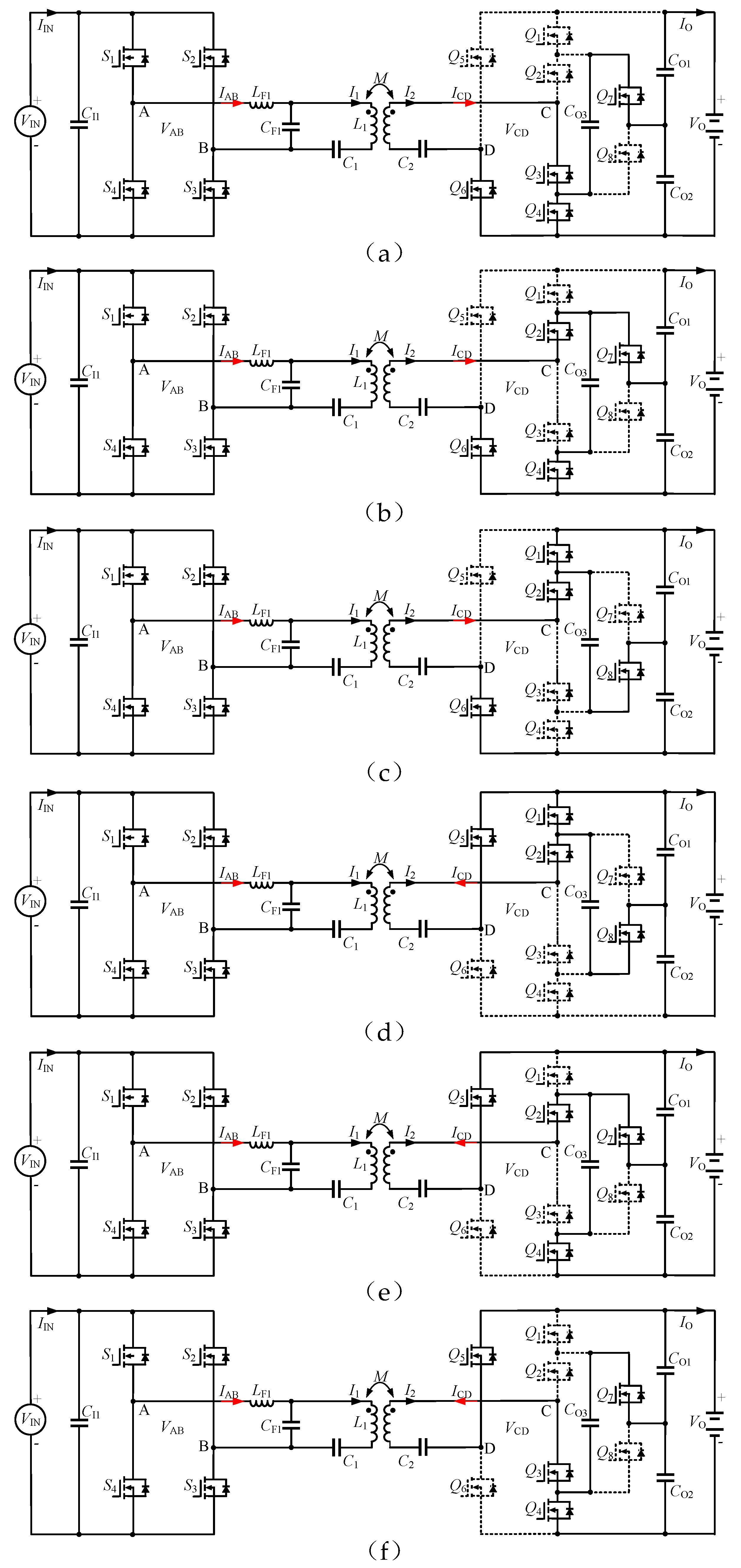
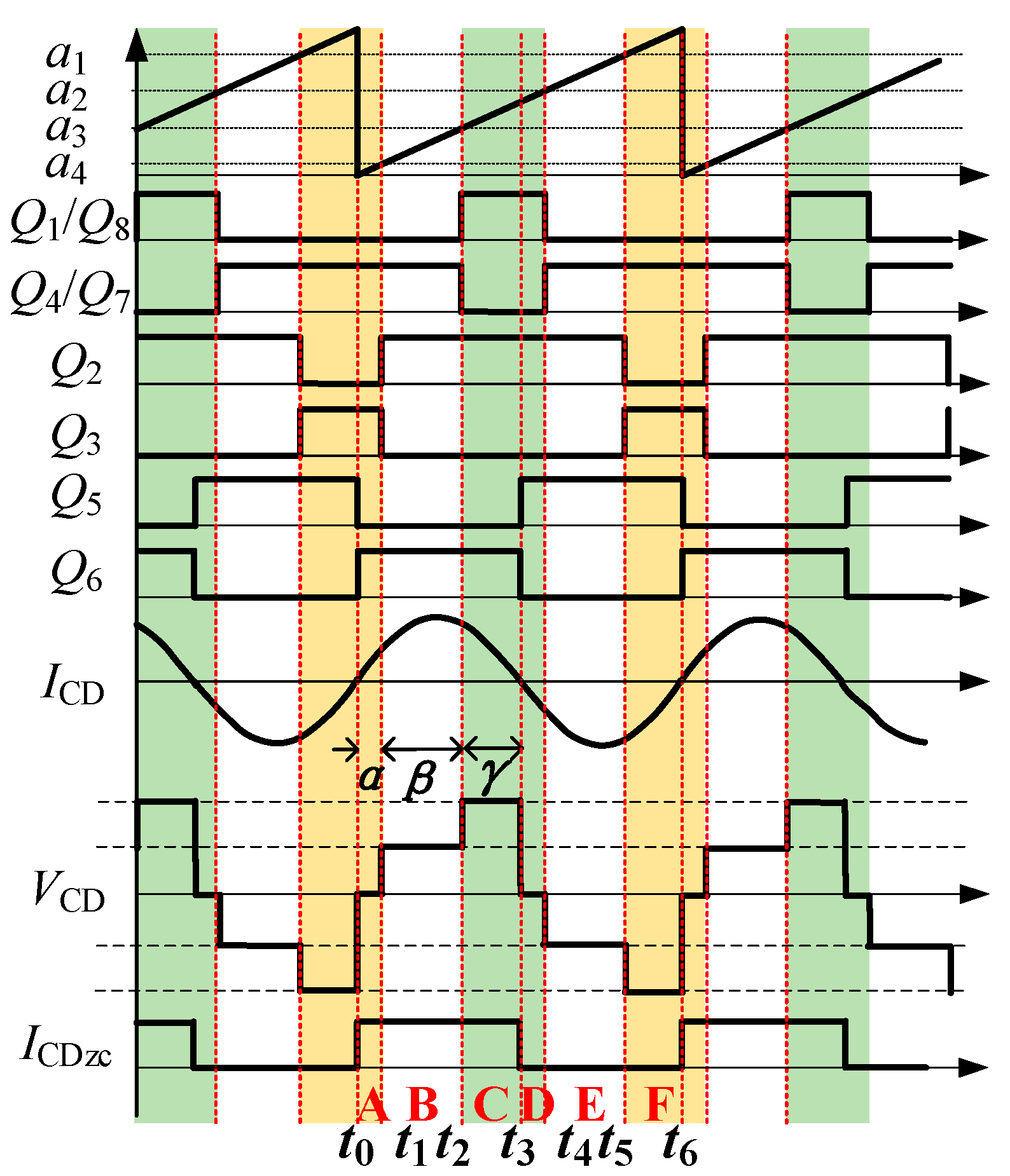
The secondary resonant current ICD is fed into the TL rectifier, as shown in Figure 1. Six modes exist in one switching cycle Ts without consideration of the dead time; the corresponding conducting circuits and key waveforms are illustrated in Figure 3 and Figure 4, respectively. Moreover, the driving signals of each MOSFET pair, i.e., Q1 and Q4, Q2 and Q3, Q5 and Q6, and Q7 and Q8, are controlled complementarily. Moreover, MOSFETs Q1 and Q8 share the same driving signal, and MOSFETs Q5 and Q6 can be replaced by diodes. VCD has five levels, i.e., 0, ±0.5VO, and ±VO, with the duration of αTs, βTs, and γTs, respectively. The sum of α, β, and γ is 0.5. The rising edge of the zero-crossing pulse ICDzc aligns with the rising edge of VCD from negative to zero at t0.
Mode A (t0–t1): VCD is zero, since the resonant network is shorted by Q3, Q4, and Q6, and the voltage of the flying capacitor CO3 is clamped to 0.5VO by connecting to CO2 in parallel;
Mode B (t1–t2): The resonant current ICD charges CO3 and CO2 through Q2, Q4, Q6, and Q7, so VCD is equal to 0.5VO;
Mode C (t2–t3): VCD is equal to VO, since the resonant current is fed to both CO1 and CO2 through Q1, Q2, and Q6, and ICD reduces to zero at t3. Moreover, the flying capacitor CO3 is connected to CO1 in parallel for the voltage clamp;
Mode D (t3–t4): ICD goes toward negative from t3, and the resonant network is shorted by Q1, Q2, and Q5; thus, VCD is equal to zero;
Mode E (t4–t5): Similar to Mode B, the negative current ICD charges CO1 instead of CO2 by flowing through Q2, Q5, and Q7;
Mode F (t5–t6): The negative current ICD proceeds toward charging both CO1 and CO2 by conducting Q3, Q4, and Q5; therefore, VCD is equal to VO. Moreover, ICD turns to zero at t6.

2.3. Voltage Gain of the TL Rectifier

The input voltage VCD of the TL rectifier is periodical in six modes and can be expressed as
V CD = { 0 0.5 V O V O 0 0.5 V O V O   ( 0.5 T s t ( α 0.5 ) T s ) ( ( α 0.5 ) T s t ( α + β 0.5 ) T s ) ( ( α + β 0.5 ) T s t 0 ) ( 0 t α T s ) ( α T s t ( α + β ) T s ) ( ( α + β ) T s t 0.5 T s )
V CD ( t ) = n = 1 [ a n cos ( 2 n π f s t ) + b n sin ( 2 n π f s t ) ] { a n = 2 f s 0.5 T s 0.5 T s V C D cos ( 2 n π f s t ) dt b n = 2 f s 0.5 T s 0.5 T s V C D sin ( 2 n π f s t ) dt
The expression in the time-domain can be obtained in (6) by the Fourier series with the Fourier coefficients an and bn. Substituting (5) into (6), the fundamental component VCD1 (t) can be derived as
V CD 1 ( t ) = V O π [ ( sin ( 2 π γ ) + sin ( 2 π α ) ) cos ( 2 n π f s t ) + ( cos ( 2 π γ ) 2 cos ( 2 π α ) ) sin ( 2 n π f s t ) ] .
V CD 1 ( t ) = V O 2 π sin ( 2 π f s t + φ ) 3 2 cos ( 2 π γ ) + 2 cos ( 2 π α ) cos ( 2 π ( α + γ ) ) φ = a r c t a n ( sin ( 2 π γ ) + sin ( 2 π α ) cos ( 2 π γ ) 2 cos ( 2 π α ) )
The sinusoidal form of (7) is rewritten in (8) with the phase angle φ, which can be recognized as the phase difference between ICD and VCD1. Thus, the root-mean-square (RMS) value of VCD1 can be obtained as V2 in (9).
V 2 = V O π 3 2 cos ( 2 π γ ) + 2 cos ( 2 π α ) cos ( 2 π ( α + γ ) ) { 0 α 0.5 0 γ 0.5
G V = V I N V O = L F M 2 2 3 2 cos ( 2 π γ ) + 2 cos ( 2 π α ) cos ( 2 π ( α + γ ) )
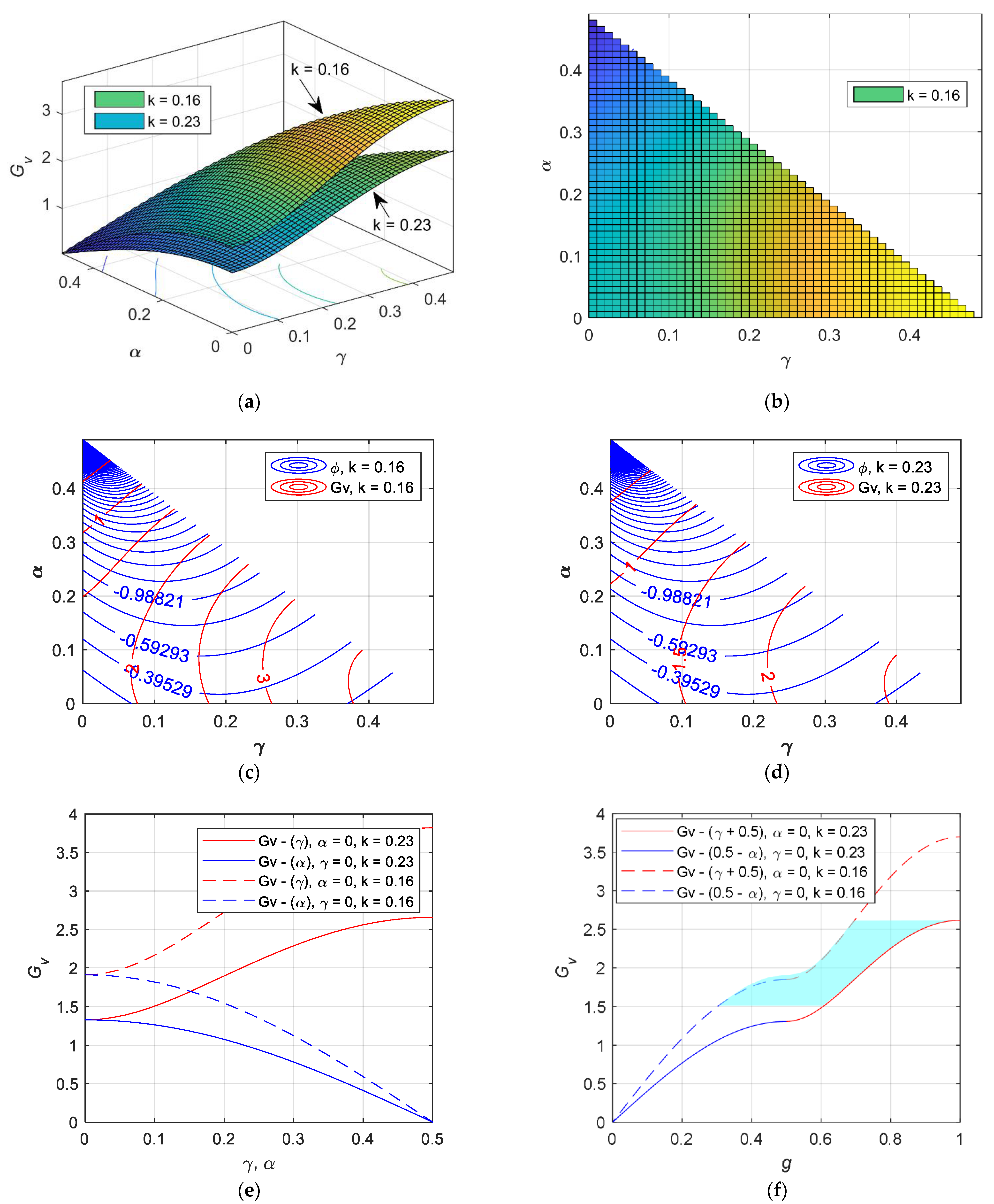
Combing (1), (4) and (9), the system voltage gain between VIN and VO can be derived in (10) approximately and plotted in Figure 5a,b, under different coupling coefficients. Figure 5a graphically shows that GV is proportional to the coupling coefficient k, and higher k results in lower GV. Moreover, both α and γ can be adopted to monotonically tune GV. Figure 5c,d show a relationship between φ and GV over various α, γ, and k. The GV trajectories in Figure 5c,d illustrate that smaller α and larger γ result in high GV, and the φ trajectories in Figure 5c,d show that the absolute value of φ becomes smaller with decreasing α. It is observed that the optimal trajectory with minimum φ follows zero α and zero γ for continuous voltage gain. The optimal trajectory of GV under different coupling coefficients is shown in Figure 5e. The optimal trajectory is marked in red for α = 0, and in blue for γ = 0. Both red curves, and blue curves interact at α = 0 and γ = 0. The optimal trajectory in Figure 5e can be represented in Figure 5f, where the operating region is highlighted in blue. To illustrate the continuous operating region of the optimal trajectory under the specified k range, the horizontal coordinate g can be formulated according to (11). The horizontal axis in the curve of GV-(γ) in Figure 5e is shifted to (0.5 + γ) in Figure 5f, and the curve of GV-(α) is mirrored at the line of α = 0.25 in Figure 5f by adopting the horizontal axis with (0.5-α), resulting in an optimal trajectory region in a closed shape.
g = { 0.5 α ( 0 g < 0.5 ) γ + 0.5 ( 0.5 g 1 )

3. Design and Implementation

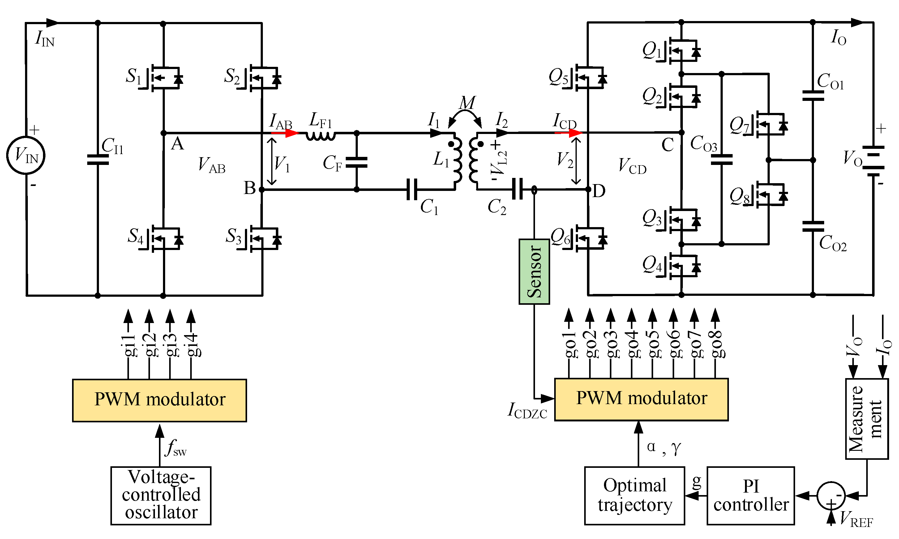
In order to achieve the desired output voltage range, a design procedure for the key parameters is proposed. In addition, the control of the inverter and rectifier is decoupled by the proposed independent control strategy without RTWFC between them. Figure 6 presents the block diagram of the proposed control strategy.

3.1. Parameter Design

Given the power level and air gap, both the transmitter coil and receiver coil are mainly limited by the physical constraints. The minimum LF can be solved from (12) with γ = 0.5 and α = 0 in (10) and should be maximized to reduce the peak current in the transmitter coil. In particular, in order to perform an inductive network for the inverter’s soft-switching, a slightly larger LF is selected [10].
L F _ m i n = V IN V O _ m i n M m a x
The resonant capacitors CF, C1, and C2 can be obtained by substituting (12) into the resonant conditions in (3).
{       C F = 1 / ( ω s 2 L F ) C 1 = C F / ( ω s 2 L 1 C F 1 ) C 2 = 1 / ( ω s 2 L 2 )

3.2. Primary Controller

As shown in Figure 6, on the transmitter side, four switches, S1, S2, S3, and S4, in the full-bridge inverter are driven by the gate signals gi1, gi2, gi3, and gi4, respectively. The gate signals gi1 and gi4 are complementary, and gi2 and gi3 are also complementary. The switching of the inverter is set to 85 kHz, which is close to the resonant frequency. The phase-shift angle of the inverter was fixed to its maximum value π . Moreover, the inverter output voltage and current are approximately in phase, due to resonant operation.

3.3. Secondary Controller

On the receiver side, eight switches—Q1, Q2, Q3, Q4, Q5, Q6, Q7, and Q8—are controlled by gate signals go1, go2, go3, go4, go5, go6, go7, and go8, respectively. As shown in Figure 4, both Q1 and Q8 share the same gate signal (go1), and Q4 and Q7 share the same gate signal (go4). The gate signals go1 and go4 are complementary. The control variables of the rectifier are the duty cycles of the zero-level voltage and one-level voltage in the TL rectifier. The output voltage is regulated by a proportional–integral (PI) controller to its desired value by adjusting the control variables according to the optimal trajectory, as shown in Figure 5f. As shown in Figure 4 and Figure 6, the receiver coil current ICD is sensed by a current transducer, and the zero-crossing signal ICDzc of ICD is obtained by a voltage comparator. All driving signals of the TL rectifier are synchronized to ICDzc. In addition, a dead-time of 200 ns is inserted in the driving signals of the MOSFET pair to enable the ZVS turn-on of the MOSFET.

4. Experimental Verification

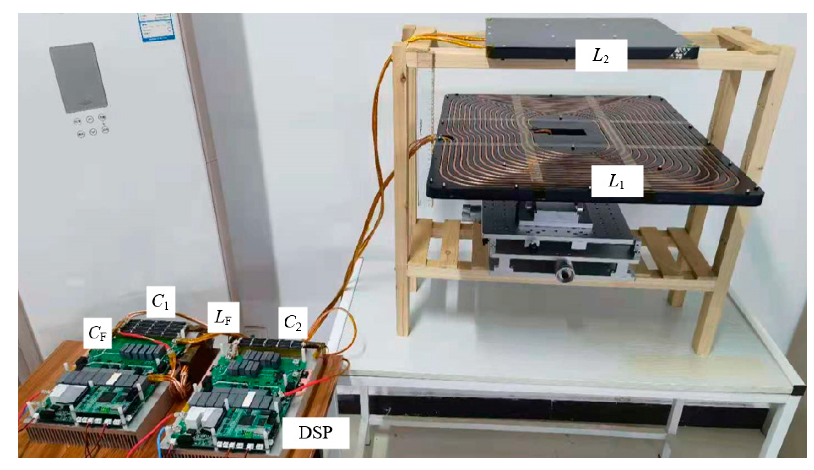
As shown in Figure 7, a 2 kW prototype was built based on the parameters in Table 2. The input voltage was 280 V, and the output voltage range was from 100 V to 200 V. Both the transmitter coil and receiver coil were fabricated according to SAE2954. Moreover, the resonant components were calculated based on the analysis in Section 3.1. The digital signal controller TMS320F28335 from TI was used to implement the control in both the transmitter and receiver. Moreover, the silicon carbide (SiC) MOSFET C3M0021120D from Cree was selected for both the inverter and rectifier. The normal operating position was horizontally aligned with a 140 mm air gap between coils in the vertical direction, and k was measured as 0.23 under such conditions. Moreover, the misaligned operating position was horizontally aligned with a 180 mm air gap between coils in the vertical direction, and the measured k became 0.16.
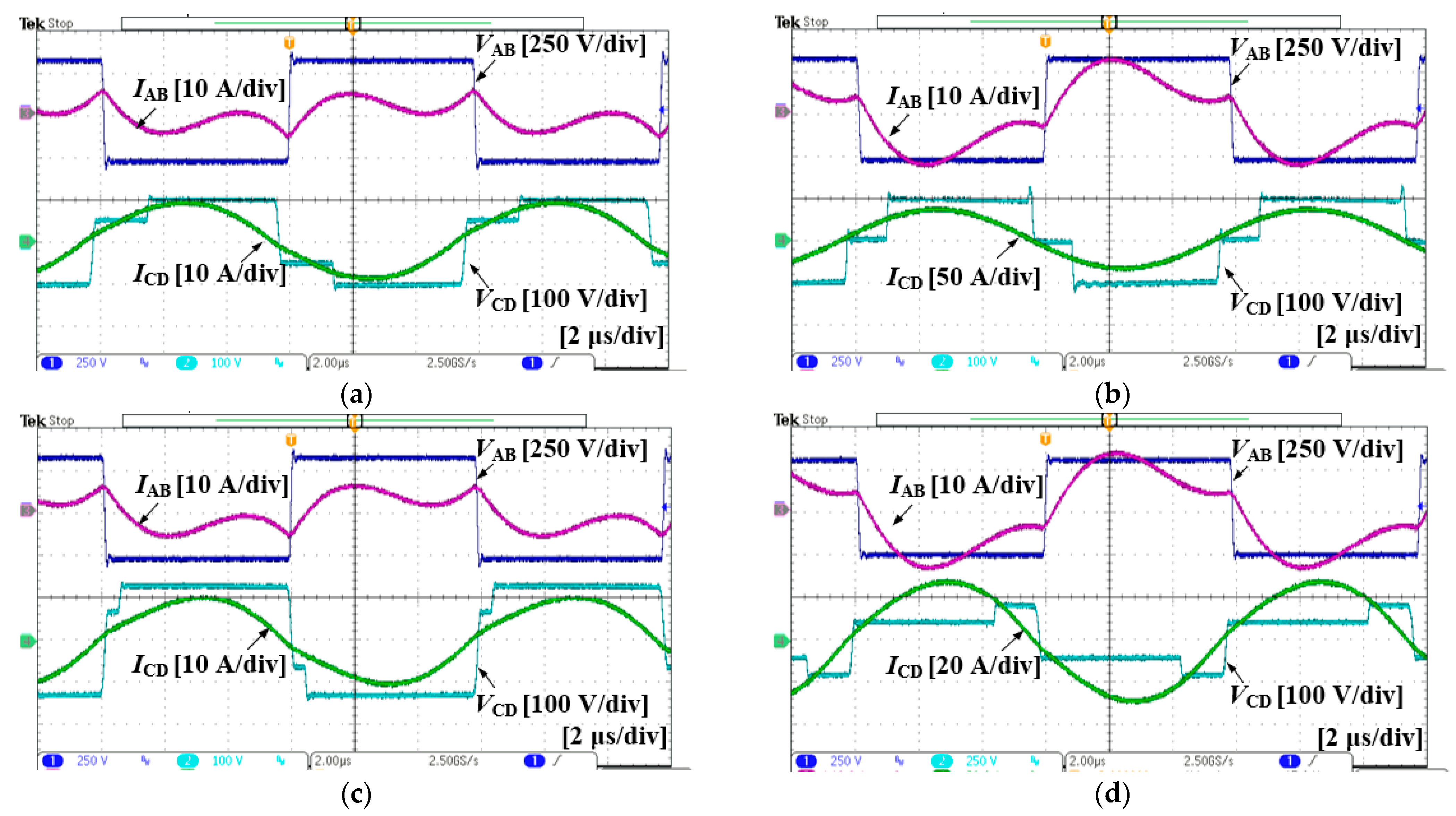
Figure 8 illustrates the operational waveforms of the inverter and TL rectifier at different output voltages in both normal positions and misalignment. The phase shift of the inverter remained at a constant of π. When k was 0.16, γ was adopted to regulate the low output voltage of 100 V, with α = 0, shown in Figure 8a, while α was utilized to tune the high output voltage of 200 V, with γ = 0, shown in Figure 8b. When k was 0.23, the output voltage was only regulated by adjusting γ, with α = 0, shown in Figure 8c,d; the larger γ corresponded to a lower output voltage. Thus, the measured waveforms of the rectifier voltage and current in Figure 8 match the optimal control trajectory in Figure 5e. The measured transient response of the load step from 7.5 A to 11.5 A is shown in Figure 9a, in which VO, IO, and ICD are captured. The output voltage presented a short settling time of 1.3 ms due to the implemented independent secondary control. In addition, the gate-source and drain-source voltage of both Q1 and Q3 were measured and are presented in Figure 9b. It is observed that no overlap exists between the falling edge of VDS and the rising edge of VGS. Thus, both Q1 and Q3 were turned on at ZVS as desired.
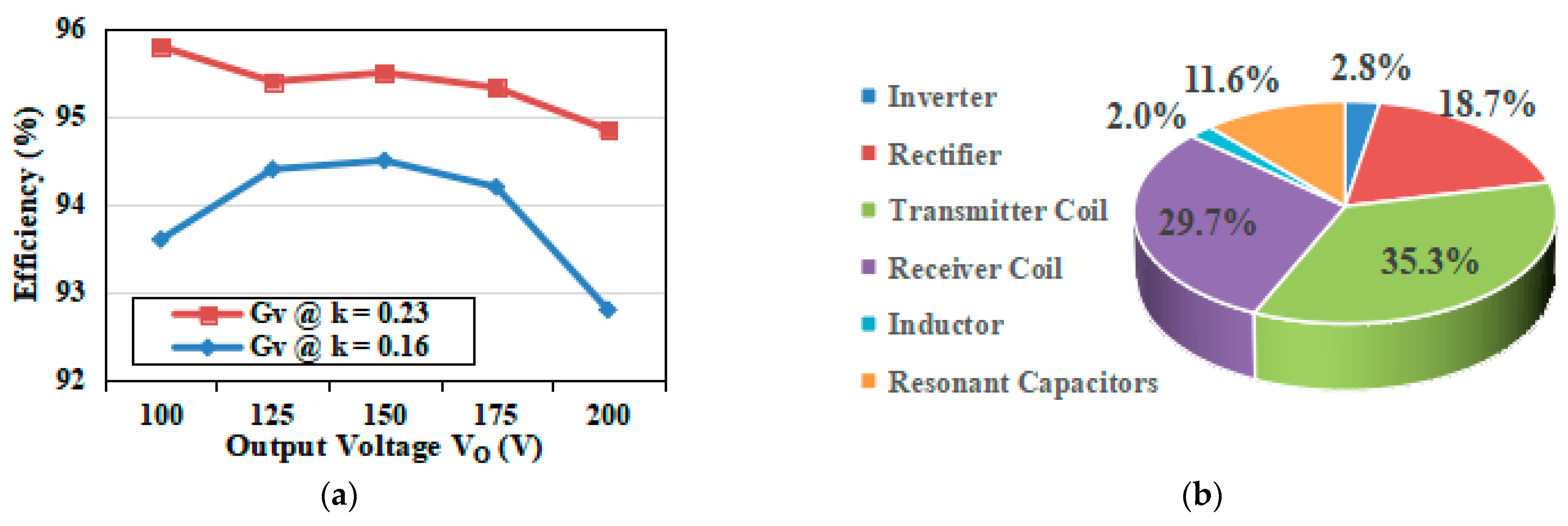
The system efficiency at full load with different k and VO was measured, which is plotted in Figure 10a. The high secondary resonant current resulted in a significant efficiency drop under misalignment. When k was 0.23, the control trajectory for the voltage gain between 1.4 and 2.8 was located on the γ axis, with α = 0, shown in Figure 5d, which is proven in Figure 8c,d. Additionally, the voltage V2 was 94 V, which is close to the minimum output voltage of 100 V. Thus, the system demonstrated the highest efficiency when the voltage conversion ratio of the TL rectifier between V2 and VO was close to one. The efficiency dropped when VO increased because the voltage conversion ratio of the TL rectifier became smaller, and the reactive power in the TL rectifier increased. When k was 0.16, the control trajectory for the voltage gain between 1.4 and 2.8 is located on the bottom left corner of the α and γ axes, shown in Figure 5c, which is proven in Figure 8a,b. The efficiency reached its lowest point at the maximum output voltage VO of 200 V because the secondary resonant network was shortened by the TL rectifier in both Modes A and D of Figure 3, when α was not zero, as shown in Figure 8b. In addition, a larger α resulted in more reactive power losses of the TL rectifier according to Figure 5c.
Conduction losses of transistors, capacitors, and coils were mainly considered to analyze the power losses in the system. The conduction losses of coils and inductor were calculated based on the measured resistance by LCR meter and measured RMS current by power analyzer PW6001. The power losses in coils were dominant according to the power loss distribution in Figure 10b. In future studies, Litz wire with more strands can be used to reduce the conduction losses of coils due to lower resistance. Moreover, more efforts can be carried out in the future to minimize the reactive power further for efficiency improvement.

5. Discussion

The experimental results presented in the previous section prove that the proposed control strategy can perform a wide output voltage regulation between 100 V and 200 V over the coupling coefficients from 0.16 to 0.23. A wide and continuous system voltage gain between the input voltage and output voltage could be achieved by tuning only one variable between α and γ, while another one remained zero, resulting in the minimization of the reactive power in the TL rectifier. Generally, a larger γ is used to reduce the output voltage monotonously for strong magnetic couplings, while α is increased to boost the output voltage under weak magnetic couplings. In addition, the experimental efficiencies at full load were measured over various output voltages. The peak efficiency was at the maximum point of γ, while the minimum efficiency was located at the maximum point of α; this is because the reactive power in the TL rectifier dominated, with a larger α.
A comparison of the key features between this study and previous publications is presented in Table 3. Using an additional DC–DC stage on the secondary side is an easy way to modulate the output voltage directly. However, an extra DC–DC stage is not desirable for the consideration of the power density and power transfer efficiency. In the literature, various compensation networks and control methods have been studied to realize the output regulation in a single-stage converter, while most of them rely on the primary control with RTWFC from the secondary side. Although a multistage converter with an extra DC–DC stage in the secondary side [25] could realize independent secondary control, the concern of power density and efficiency cannot be addressed. Moreover, the ability of the output voltage regulation is limited by the phase shift of the full-bridge active rectifier. Hence, previous studies fail to achieve a balance among features, such as wide output voltage regulation, independent secondary control, and various magnetic couplings. Compared with the previous studies, all the key features presented in Table 3 can be realized in a single-stage converter based on the proposed control strategy.

6. Conclusions

In this paper, a control strategy of the TL rectifier was proposed for wide output voltage regulation with minimization of reactive power for the LCC/S-compensated IPT system. The voltage gains of the LCC/S compensation network, TL rectifier, and the system were derived in a generic analytical expression and analyzed in detail. The operating principle of the TL rectifier was explained by circuit diagrams and waveforms. In addition, a design procedure of key parameters and an optimal control trajectory for reactive power minimization were provided to design and control a 2 kW prototype. The voltage range between 100 V and 200 V was achieved in both aligned (k = 0.23) and misaligned (k = 0.16) positions by modulating the duty cycles of zero-level and one-level voltage in the TL rectifier. The prototype realized a wide output regulation between 100 V and 200 V, demonstrated a fast response with a settling time of 1.3 ms, and presented a peak DC–DC efficiency of 95.8% at the low output voltage of 100 V. Future research will be carried out to include the bidirectional power transfer and efficiency optimization.

Author Contributions

Conceptualization, J.L. (Jianting Li); methodology, J.L. (Jianke Li); validation, J.L. (Jianting Li), J.C. and P.W.; writing—review and editing, J.L. (Jianting Li), P.W., S.C. and J.W.; supervision, J.W. All authors have read and agreed to the published version of the manuscript.

Funding

This research received no external funding.

Conflicts of Interest

The authors declare no conflict of interest. The funders had no role in the design of the study; in the collection, analyses, or interpretation of data; in the writing of the manuscript; or in the decision to publish the results.

References

  1. Zhao, L.; Thrimawithana, D.; Madawala, U. Hybrid bidirectional wireless EV charging system tolerant to pad misalignment. IEEE Trans. Ind. Electron. 2017, 64, 7079–7086. [Google Scholar] [CrossRef]
  2. Qu, X.; Zhang, W.; Wong, S.; Tse, C. Design of a current-source-output inductive power transfer LED lighting system. IEEE J. Emerg. Sel. Top. Power Electron. 2015, 3, 306–314. [Google Scholar]
  3. Bito, J.; Jeong, S.; Tentzeris, M. A real-time electrically controlled active matching circuit utilizing genetic algorithms for wireless power transfer to biomedical implants. IEEE Trans. Microw. Theory Tech. 2016, 64, 365–374. [Google Scholar] [CrossRef]
  4. Bian, B.; Wei, Y.; Li, Y. Key Technologies for the Application of the Electric Propulsion System on the GEO Satellite Platform. Meas. Control. 2008, 41, 85–87. [Google Scholar]
  5. Liu, Y.; Sun, Y.; Su, M.; Zhou, M.; Zhu, Q.; Li, X. A single-phase PFC rectifier with wide output voltage and low-frequency ripple power decoupling. IEEE Trans. Power Electron. 2018, 33, 5076–5086. [Google Scholar] [CrossRef] [Green Version]
  6. Wang, Y.; Wei, G.; Dong, S.; Dong, Y.; Yu, X.; Li, X. A High-Efficiency Self-Synchronous RF–DC Rectifier Based on Time-Reversal Duality for Wireless Power Transfer Applications. Electronics 2022, 11, 90. [Google Scholar] [CrossRef]
  7. Lu, M.; Ngo, K. Systematic design of coils in series–series inductive power transfer for power transferability and efficiency. IEEE Trans. Power Electron. 2018, 33, 3333–3345. [Google Scholar] [CrossRef]
  8. Cheng, B.; He, L. Realize Load-Independent Output with Soft Switching Based on Switched Capacitor for Wireless Charger System. IEEE Access 2022, 10, 10094–10104. [Google Scholar] [CrossRef]
  9. Simonazzi, M.; Campanini, A.; Sandrolini, L.; Rossi, C. Design Procedure Based on Maximum Efficiency for Wireless Power Transfer Battery Chargers with Lightweight Vehicle Assembly. Energies 2022, 15, 70. [Google Scholar] [CrossRef]
  10. Li, S.; Li, W.; Deng, J.; Nguyen, T.; Mi, C. A double-sided LCC compensation network and its tuning method for wireless power transfer. IEEE Trans. Veh. Technol. 2015, 64, 2261–2273. [Google Scholar] [CrossRef]
  11. Lu, J.; Zhu, G.; Lin, D.; Zhang, Y.; Jiang, J.; Mi, C. Unified Load-Independent ZPA Analysis and Design in CC and CV Modes of Higher Order Resonant Circuits for WPT Systems. IEEE Trans. Transp. Electric 2019, 5, 977–987. [Google Scholar] [CrossRef]
  12. Zhang, L.; Li, H.; Guo, Q.; Xie, S.; Yang, Y. Research on Constant Voltage/Current Output of LCC–S Envelope Modulation Wireless Power Transfer System. Energies 2022, 15, 1562. [Google Scholar] [CrossRef]
  13. Wu, H.; Gilchrist, A.; Sealy, K.; Bronson, D. A High Efficiency 5 kW Inductive Charger for EVs Using Dual Side Control. IEEE Trans. Indust. Inform. 2012, 8, 585–595. [Google Scholar] [CrossRef] [Green Version]
  14. Kim, M.; Joo, D.; Lee, B. Design and Control of Inductive Power Transfer System for Electric Vehicles Considering Wide Variation of Output Voltage and Coupling Coefficient. IEEE Trans. Power Electron. 2019, 34, 1197–1208. [Google Scholar] [CrossRef]
  15. Stoyka, K.; Vitale, A.; Costarella, M.; Avella, A.; Pucciarelli, M.; Visconti, P. Development of a Digitally Controlled Inductive Power Transfer System with Post-Regulation for Variable Load Demand. Electronics 2022, 11, 58. [Google Scholar] [CrossRef]
  16. Zhang, Y.; Kan, T.; Yan, Z.; Mi, C. Frequency and Voltage Tuning of Series–Series Compensated Wireless Power Transfer System to Sustain Rated Power Under Various Conditions. IEEE J. Emerg. Sel. Top. Power Electron. 2019, 7, 1311–1317. [Google Scholar] [CrossRef]
  17. Hu, H.; Cai, T.; Duan, S.; Zhang, X.; Niu, J.; Feng, H. An optimal variable frequency phase shift control strategy for ZVS operation within wide power range in IPT systems. IEEE Trans. Power Electron. 2020, 35, 5517–5530. [Google Scholar] [CrossRef]
  18. Wireless Power Transfer for Light-Duty Plug-In/Electric Vehicles and Alignment Methodology. Available online: https://www.sae.org/standards/content/j2954_201904/ (accessed on 20 October 2020).
  19. Wang, X.; Xu, J.; Leng, M.; Ma, H.; He, S. A Hybrid Control Strategy of LCC-S Compensated WPT System for Wide Output Voltage and ZVS Range with Minimized Reactive Current. IEEE Trans. Ind. Electron. 2021, 68, 7908–7920. [Google Scholar] [CrossRef]
  20. Zhang, J.; Zhao, J.; Zhang, Y.; Deng, F. A Wireless Power Transfer System with Dual Switch-Controlled Capacitors for Efficiency Optimization. IEEE Trans. Power Electron. 2019, 35, 6091–6101. [Google Scholar] [CrossRef]
  21. Li, Z.; Liu, H.; Tian, Y.; Liu, Y. Constant Current/Voltage Charging for Primary-Side Controlled Wireless Charging System Without Using Dual-Side Communication. IEEE Trans. Power Electron. 2021, 36, 13562–13577. [Google Scholar] [CrossRef]
  22. Wu, L.; Zhang, B.; Jiang, Y. Position-Independent Constant Current or Constant Voltage Wireless Electric Vehicles Charging System Without Dual-Side Communication and DC–DC Converter. IEEE Trans. Ind. Electron. 2022, 69, 7930–7939. [Google Scholar] [CrossRef]
  23. Iam, I.-W.; Hoi, I.-U.; Huang, Z.; Gong, C.; Lam, C.-S.; Mak, P.-I.; Da Silva Martins, R.P. Constant-Frequency and Non-Communication-Based Inductive Power Transfer Converter for Battery Charging. IEEE J. Emerg. Sel. Top. Power Electron. 2020, 10, 2147–2162. [Google Scholar] [CrossRef]
  24. Jiang, T.; Zhang, J.; Wu, X.; Sheng, K.; Wang, Y. A Bidirectional Three-Level LLC Resonant Converter with PWAM Control. IEEE Trans. Power Electron. 2016, 31, 2213–2225. [Google Scholar] [CrossRef]
  25. Li, K.; Tan, S.; Hui, S. Overshoot Damping and Dynamics Improvement in Wireless Power Transfer Systems Via Receiver-Side Controller Design. IEEE Trans. Power Electron. 2022, 37, 2362–2371. [Google Scholar] [CrossRef]
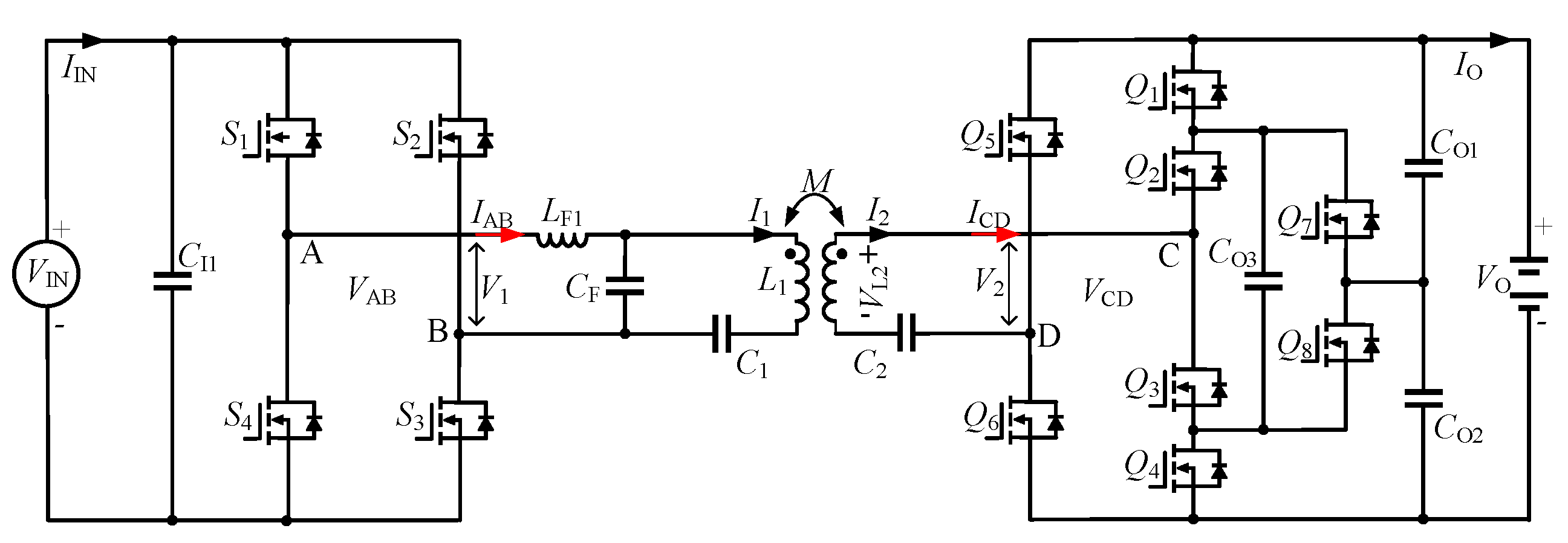
Figure 1. Circuit topology of the LCC/S-compensated IPT with TL rectifier.
Electronics 11 01426 g001
Figure 2. Equivalent circuit of the converter.
Electronics 11 01426 g002
Figure 3. Operating modes in one switching cycle: (a) Mode A, (b) Mode B, (c) Mode C, (d) Mode D, (e) Mode E, and (f) Mode F.
Electronics 11 01426 g003
Figure 4. Key waveforms of the TL rectifier.
Electronics 11 01426 g004
Figure 5. The voltage gain of TL rectifier: (a) a 3D plot of voltage gain for k = 0.23 and 0.16; (b) a 2D plot of voltage gain for k = 0.16; (c) plot of GV and φ for k = 0.16; (d) plot of GV and φ for k = 0.23; (e) plot of GV in optimal trajectory; (f) plot of GV operating region in optimal trajectory.
Electronics 11 01426 g005
Figure 6. Block diagram of the control strategy.
Electronics 11 01426 g006
Figure 7. Photo of the prototype. L1: Transmitter coil; L2: Receiver coil; C1, CF: Resonant capacitors on the transmitter side; LF: Resonant inductor on the transmitter side; C2: Resonant capacitor on the receiver side; DSP: digital signal processor TMS TMS320F28335.
Electronics 11 01426 g007
Figure 8. Measured waveforms of inverter and rectifier: (a) V O = 100   V ,   k = 0.16 ; (b) V O = 200   V ,   k = 0.16 ; (c) V O = 100   V ,   k = 0.23 ; (d) V O = 200   V ,   k = 0.23 .
Electronics 11 01426 g008
Figure 9. Measured waveforms: (a) transient response and (b) soft-switching.
Electronics 11 01426 g009
Figure 10. Measured efficiency (a) and power losses distribution (b) at 150 V, k = 0.16.
Electronics 11 01426 g010
Table 1. Definition of the key symbols.
SymbolDescription
αDuty cycle of zero-level voltage in the TL rectifier
βDuty cycle of half-level voltage in the TL rectifier
γDuty cycle of one-level voltage in the TL rectifier
φPhase difference between ICD and VCD1
TsSwitching period
VAB, IABInverter output voltage and current
VCD, ICDRectifier input voltage and current
VCD1Fundament component of VCD
ICDZCZero-crossing pulse signal of ICD
V1Fundament component in RMS of VAB
V2Fundament component in RMS of VCD
I1RMS current in the transmitter coil
I2RMS current in the receiver coil
VINInput DC voltage
VOOutput DC voltage
L1Inductance of the transmitter coil
L2Inductance of the receiver coil
LFInductance of the series resonant inductor in transmitter
CFCapacitance of the parallel resonant capacitor in transmitter
C1Capacitance of the series resonant capacitor in transmitter
C2Capacitance of the series resonant capacitor in receiver
S1, S2, S3, S4Switches in the inverter
Q1, Q2, Q3, Q4, Q5, Q6, Q7, Q8Switches in the TL rectifier
Table 2. List of circuit parameters.
L1L2LFCFC1C2VINVO
44 µH61 µH32 µH122 nF222 nF57.5 nF280 V100–200 V
Table 3. Comparison with studies in the literature.
ReferenceCompensationNo Extra DC–DCActive RectifierNo Wireless Feedback CommunicationVO Range
(V)
k Range
[15]SS×××120.34–0.75
[16]SS××1200.16–0.54
[19]LCC/S××100–1800.15–0.2
[20]SS×65–1300.12
[22]SS×CC/CV0.1–0.43
[23]SS60–1700.255
[25]SS××15.3–19.2-
This studyLCC/S100–2000.16–0.23
√: yes. ×: no.
Publisher’s Note: MDPI stays neutral with regard to jurisdictional claims in published maps and institutional affiliations.