Article

A Novel Improved Coordinate Rotated Algorithm for PWM Rectifier THD Reduction

School of Information Engineering, Southwest University of Science and Technology, Mianyang 621010, China
*
Author to whom correspondence should be addressed.
Electronics 2022, 11(9), 1435; https://doi.org/10.3390/electronics11091435
Submission received: 11 April 2022 / Revised: 25 April 2022 / Accepted: 26 April 2022 / Published: 29 April 2022
(This article belongs to the Section Power Electronics)

Abstract

:
In this paper, a novel algorithm with a rotating coordinate system is proposed to improve the total harmonic distortion (THD) of PWM rectifiers. Aiming at solving the disadvantages of poor dynamic response, unstable switching frequency, and a large calculation burden in some current control methods, the proposed method employs the rotating coordinate system to control the active current and reactive current separately while modifying the calculation error. The proposed method is verified through a single-phase PWM rectifier. Based on the measured results and compared with many other algorithms, such as the peak current mode control (PCMC), average current mode control (ACMC), one cycle control (OCC), and modulating duty ratio (MDR), the proposed method not only effectively reduces the intermediate variables during calculation, but also improves the THD and reliability of the circuit. The proposed method can be applied in single-phase PWM rectifiers applied in household-distributed energy storage systems.

1. Introduction

In recent years, the development and improvement of new energy have attracted much attention. Many new energy resources have great potential to compete with traditional power sources. However, new energy sources can make power generation unstable and lower the power factor. In order to solve that problem, many new energy distributed generation systems are equipped with energy storage devices for suppressing power fluctuations, peak clipping, and energy scheduling [1,2,3,4,5,6,7,8]. Pulse width modulation (PWM) rectifiers are widely used in new energy storage devices and have become an important component between energy storage devices and the power grid [9,10,11,12,13,14,15]. The block diagram of the hybrid power generation system of new energy and energy storage devices is shown in Figure 1. Electric energy is distributed through high-voltage transmission lines, transformers, and power distribution cabinets. The rectifiers modulate the electric energy and finally transmit it to electrical equipment.
A low power factor will cause the grid and equipment not to be fully utilized. It can increase the burden on the grid and additional line losses. At present, all countries have mandatory requirements for the power factor of electrical equipment. In order to achieve unity power factor and a low harmonic current of electrical equipment, rectifier equipment began to use Power Factor Correction (PFC) technology. Among them, passive PFC passively reduces current distortion and current harmonics by connecting capacitors, series inductors, diodes, and other components in parallel in the rectifier loop. Passive PFC has a simple structure, high reliability, and no electromagnetic interference (EMI). However, the current distortion correction capability of passive PFC is limited, and it is gradually replaced by active PFC. Active PFC modulates the Boost circuit through PWM, so that the grid-side current waveform follows the grid-side voltage waveform, thereby eliminating current harmonics and achieving a unity power factor. Compared with passive PFC, the correction effect is much better than that of passive PFC. Compared with the traditional PFC circuit, this kind of circuit has the following characteristics: 1. There is an uncontrollable rectifier bridge in the front stage of the traditional PFC circuit, and the energy loss of the uncontrollable rectifier bridge is very high, resulting in low overall transmission efficiency. 2. More PFC circuit devices and lower transmission efficiency 3. The circuit designed in this design is more controllable, with a lower THD value and higher PF value.
In rectification techniques, due to the stable voltage of the support capacitor, the forward conduction time of the rectifier diode accounts for a small proportion of the entire AC half-wave cycle. Therefore, the input current often has a very short-time and high-peak current spike [16,17,18,19,20,21]. The current suddenly changes at the moment when the transistor is triggered and turned on, which will not only cause current distortion and harmonic pollution but also reduce the power factor. Moreover, it causes additional energy losses which can result in some other problems such as overheating, local resonance, overvoltage, and overcurrent [22,23,24,25,26,27].
In order to solve this problem, many researchers have proposed different methodologies such as peak current mode control (PCMC), average current mode control (ACMC), and one cycle control (OCC) [28,29,30,31,32,33,34]. For PCMC, when the switching period starts, the transistor is switched on and the voltage drop across the inductance is positive. Therefore, its current will increase accordingly. This current is compared to the control current provided by the voltage loop regulator, and when the inductance current reaches the transistor, it is switched off, and the inductance current slope becomes negative. The main drawback of this control technique is its noise susceptibility, which may cause a premature reset of the latch. Consequently, the appearance of subharmonic oscillations may lead to instabilities. For ACMC, it requires that the total waveform of the current be reconstructed for the control loop. Therefore, the comparison between the sawtooth waveform and the amplified error output takes place more than once in each switching period resulting in subharmonic oscillations. This drawback cannot be ignored, especially for rectifiers. As for OCC, it can be used in both halves of the supply voltage. This method is a non-linear control technique to control the duty ratio of the switch in real-time. However, in each half cycle, the average value of the chopped waveform is made equal to the reference value resulting in a greater response. The modulating duty ratio method (MDR) has also been proposed. The THD of the utility line currents depends on the amplitude and phase-shift of the six-order component injected to the duty ratio of the boost converter.
Still, some other new technologies have also been proposed in recent years. [35] proposed an electro-thermal model. It incorporates in the same simulation environment in both models of the electrical and thermal behavior of switching devices. The validation of the models and control loops is also enhanced by an exhaustive robustness analysis of the parametric variations of the model with respect to the nominal case. [36] proposed a formal verification and co-simulation method which can be applied in an industrial setting. [37] proposed adaptive controller exploiting learning concepts which takes the ideas from the theory of adaptive control techniques and the theory of statistical learning at the same time. It can ensure trajectory tracking while allowing for disturbance rejection with different disturbance signal amplitudes.
This paper designs an improved predictive current control algorithm under the rotating coordinate system. The proposed method can achieve the same frequency and phase of the grid-side current and grid-side voltage, unit power factor, fast current response, and lower harmonic current. The basic principle is to decouple the dq-axis current of the input AC into active current and reactive current. At the same time, on the basis of the current decoupling control, the predictive current control strategy is further simplified and improved. The active current and reactive current are precisely controlled.
This paper is organized as follows:
Section 1 is the introduction, which mainly introduces the research background and significance of the single-phase PWM rectifier and analyzes the research status of its topology and control strategy in recent years.
Section 2 studies the control strategy of the single-phase PWM rectifier. Since the control strategy is the key to the single-phase PWM rectifier, the appropriate control method is the guarantee the performance of the single-phase PWM rectifier. Aiming at some existing problems, an improved current control strategy based on a rotating coordinate system is proposed. The mathematical model is established, and the current instantaneous control algorithm of the single-phase PWM rectifier is deduced.
Section 3 is the main circuit parameter calculation. Specifically, it includes a detailed analysis and calculation of the AC-side inductance and DC-side capacitance under the rated parameters of the system.
Section 4 is the system simulation analysis. The simulation is performed on the MATLAB/SIMULINK platform. The calculated circuit parameters are input into the simulation to verify the simulation effects of the proposed current control algorithm with three other current control algorithms. The simulation proves that the proposed algorithm can achieve a low THD with unit power factor correction.
Section 5 is the design of the circuit and test of the experimental platform. The experimental platform is built for an experimental demonstration to test the effectiveness of the proposed current control algorithm.
Section 6 is the conclusion, which completes the whole paper.

2. Theory and Derivation

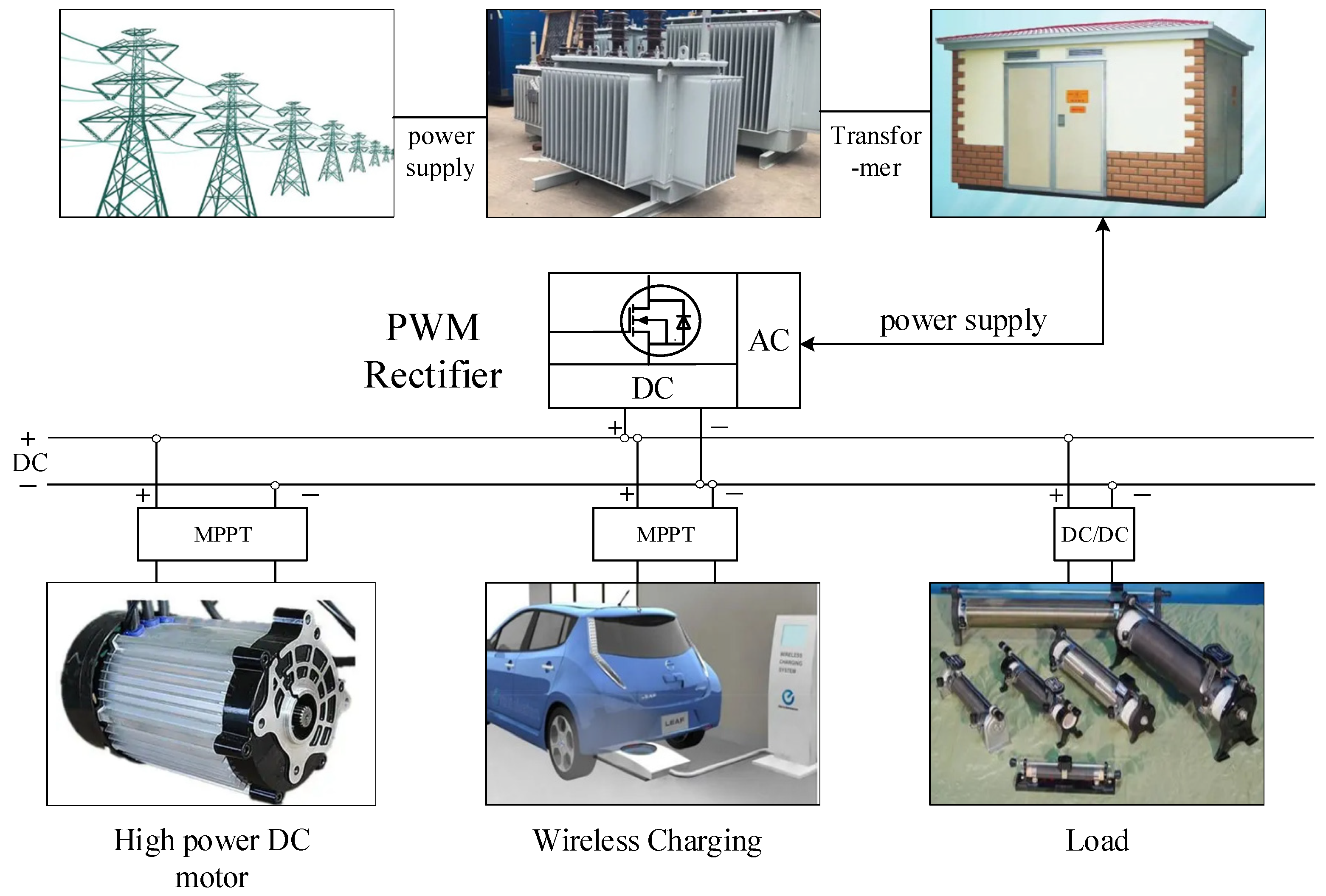
2.1. The Structure of a PWM Rectifier

The topology of the single-phase PWM rectifier is shown in Figure 2. The topology is mainly composed of a Boost inductor and four fully controlled power switching devices. Us is the AC input voltage; Uo is DC output voltage; is is the input current; LS is the input boost inductor; RS is the equivalent resistance; CB is the output filter capacitor; RL is the output load; and the controller controls are S1, S2, S3, and S4 through the PWM signal with on and off states to achieve rectification and PFC.

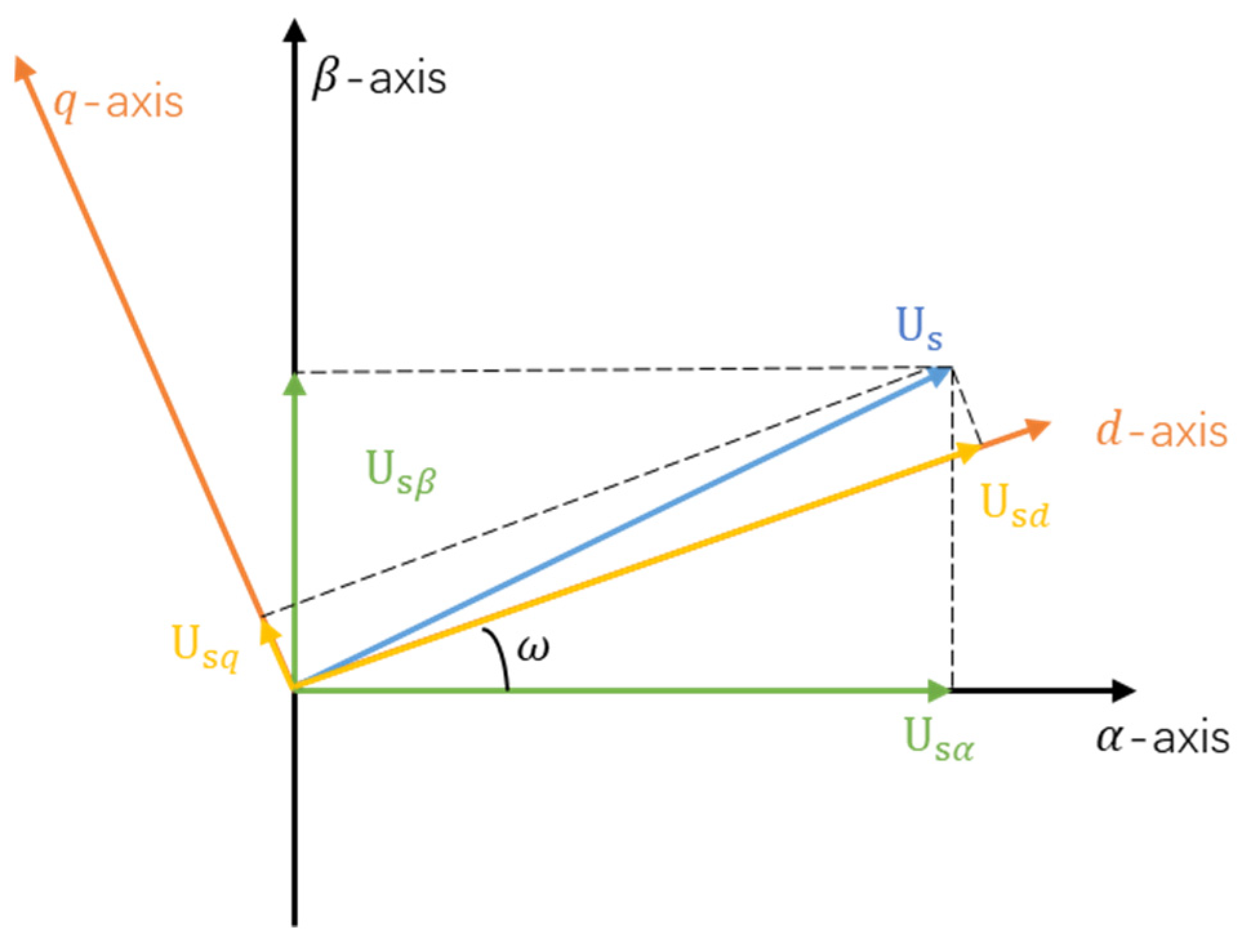
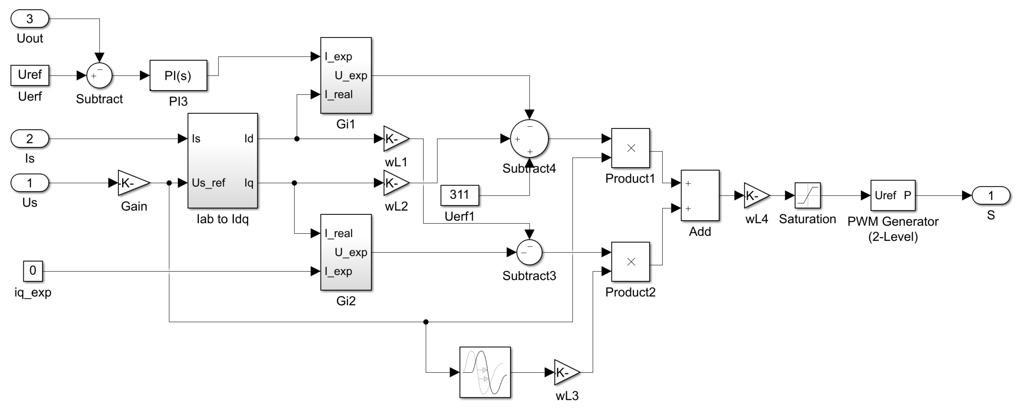
2.2. d-q Axis Current Decoupling Control

There are several common algorithms being used. The triangular wave comparison method can fix the switching frequency, but the PI controller is used in the current inner loop. There is also a a steady-state current error. It fluctuates in a sinusoidal cycle, so when the current inner loop adopts the PI controller to track and control the fast-changing sinusoidal signal, the system is theoretically a differential system. At the same time, when the load is suddenly changed, the stability of the triangular wave comparison method is poor. These shortcomings limit its application in high-stability applications. The hysteresis comparison method has a simple control method and a fast system response speed, but the switching frequency is not fixed. The wide distribution of harmonics is not conducive to the design of filters. The predictive current control has the characteristics of a fixed switching frequency and high dynamic performance, but due to a large amount of calculations, the sampling time and calculation time will lead to delay errors. Therefore, in view of the above problems, this paper designs an improved predictive current control algorithm under the rotating coordinate system to achieve the same frequency and phase of the grid-side current and grid-side voltage, unit power factor, fast current response, and lower harmonic current. The basic principle is to decouple the d-q axis current of the input AC into active current and reactive current. At the same time, based on the current decoupling control, the traditional predictive current control strategy is further simplified and improved. The active current and reactive current are precisely controlled. In this case, the design of the decoupler network for a process is obtained by specifying n elements of the decoupler or the n desired transfer functions of the apparent process. The most extended forms of conventional decoupling are termed ideal and simplified decoupling.
According to the power calculation, the three-phase voltage and current vectors are subjected to the Park transformation or Clarke transformation to obtain the instantaneous power of the system. To convert the single-phase system structure into a three-phase system, it is necessary to lead and lag the single-phase AC voltage us by 120° to obtain ua and ub. Then the three-phased voltages can be expressed as
{ u s = 2 U sin ( ω t ) u a = 2 U sin ( ω t 120 ° ) u b = 2 U sin ( ω t + 120 ° )
where U is the effective value of the phase voltage. In order to construct the three-phased current, we can set the grid-side current is = ic with a lead and lag of 120°, respectively, to obtain ia and ib. The grid-side current is contains many n-th harmonic currents, and then the three-phased currents can be expressed as
{ i c = 2 n = 1 I n sin ( n ω t + θ n ) i a = 2 n = 1 I n sin [ ( n ω t 120 ° ) + θ n ] i b = 2 n = 1 I n sin [ ( n ω t + 120 ° ) + θ n ]
where In is the effective value of each harmonic current and θn is the initial phase of each harmonic current. Then, the correspondence between the three-phase coordinate system a-b-c and the two-phase coordinate system x-y can be established, as shown in Figure 3.
In the coordinate systems, the a-b-c coordinate axes form a 120° phase angle. The x-y coordinate axes form a 90° phase angle. The a-axis superimposes with the x-axis. The effective turn number of each phase winding of the three-phase coordinate system is set to be N3. The current of each phase are ic, ia, and ib, respectively. The effective number of turns of each phase of the two-phase coordinate system is set to be N2 and the currents of each phase are ix and iy, respectively. Subsequently, through the definition of active current and reactive current, the two-phase plane coordinate system can be transformed into the d-q coordinate system to control the overall power. This algorithm is sensitive to grid-side harmonics. When the side harmonics are large, it is difficult to obtain the correct system parameters.
The essence of the algorithm for constructing the coordinate system is to imitate the composition of the three-phase system. After the three-phase coordinate system is constructed, it is still necessary to perform a triangular transformation and convert it to the x-y coordinate axis. Therefore, the grid-side voltage and current can be directly lagged by a 90° phase angle to form an orthogonal virtual voltage and current. After superimposing the two, the vectors of us and is can be obtained which can be calculated directly, as shown in Figure 4.
In practical applications, the grid-side current is in the single-phase system and the PWM rectifier AC-side voltage uon have a lag of 90°. Then, in the α-β static coordinate system, the voltage and current can be expressed as
{ u s α = u s = 2 U cos ( ω t ) u s β = 2 U sin ( ω t )
{ i s α = i s = 2 I cos ( ω t φ ) i s β = 2 I sin ( ω t φ )
where usα and usβ are the components of the grid-side voltage in the α-β static coordinate system; isα, isβ are the components of the grid-side current in the α-β static coordinate system; and φ is the initial phase of the grid-side current. Through the Park transformation, the components of grid-side voltage and current in the α-β static coordinate system are converted into the components in the d-q rotating coordinate system which can be expressed as
[ u s d u s q ] = [ cos ( ω t ) sin ( ω t ) sin ( ω t ) cos ( ω t ) ] [ u s α u s β ]
[ i s d i s q ] = [ cos ( ω t ) sin ( ω t ) sin ( ω t ) cos ( ω t ) ] [ i s α i s β ]
where usd, usq are the components of the grid-side voltage in the d-q rotating coordinate system and isd, isq are the grid-side current components in the d-q rotating coordinate system. The improved predictive current control adopts a virtual orthogonal coordinate system. The model of the single-phase PWM rectifier in the α-β static coordinate system can be obtained as
{ d i s α d t = 1 L ( u s α u a b α R S i s α ) d i s β d t = 1 L ( u s β u a b β R S i s β )
where uabα and uabβ are the components of the grid-side voltage in the α-β static coordinate system. Through the conversion relationship, the mathematical model in the d-q rotating coordinate system can be expressed as
{ d i s d d t = 1 L ( u s d u a b d ) ω i s q d i s q d t = 1 L ( u s q u a b q ) + ω i s d
The control variable can realize the decoupling control of active current and reactive current. The specific control block diagram is shown in Figure 5, where Gci(s) is the current of the d-axis and the q-axis in the inner loop controllers.

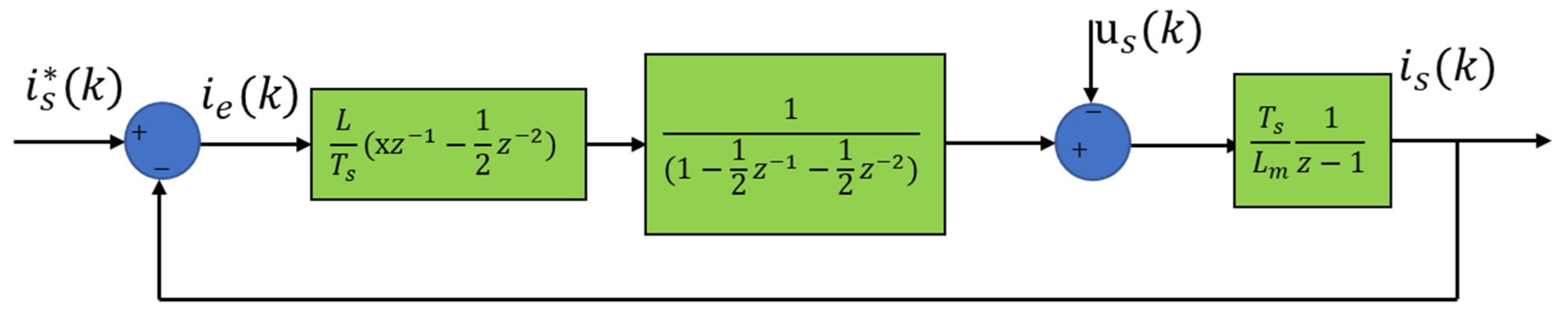
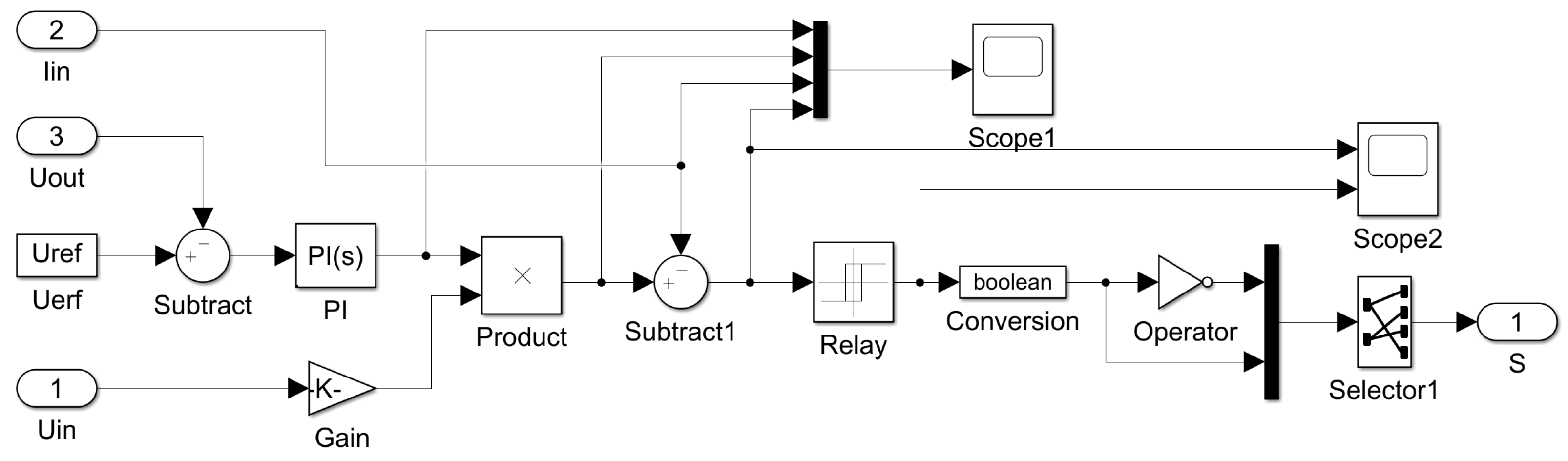
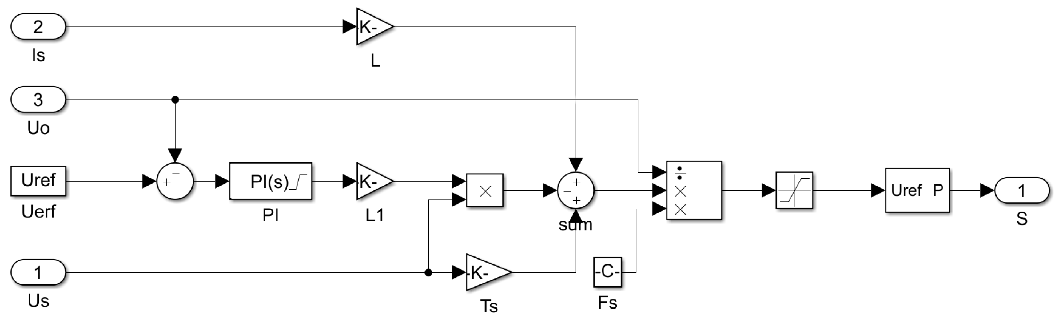
2.3. Predictive Current Control Strategy Improvement

The predictive current control algorithm is to discretize voltage and current. Since the discrete time is very short, the predicted current on the grid-side in the next cycle can be calculated as
{ i s d ( k ) = T s L [ u s d ( k 1 ) u a b d ( k 1 ) ] ω T s i s q ( k 1 ) + i s d ( k 1 ) i s q ( k ) = T s L [ u s q ( k 1 ) u a b q ( k 1 ) ] + ω T s i s d ( k 1 ) + i s q ( k 1 )
where Ts is the switching period of the bridge circuit in the PWM rectifier.
The basic idea of the current prediction strategy is to sample the grid-side current is at the beginning of each switching cycle; the reference value is of the current at the beginning of the next cycle can be predicted. Then, from the difference isis, is can be set equal to is at the beginning of the next cycle. This method has the characteristics of fixed switching frequency and fast dynamic response, but the computation is relatively complicated.
Since sampling and calculation will lead to the delay error of system control, to solve this problem, the control target of the controller is set as the current at the k + 1th sampling point equal to the end of the switching cycle [k, k + 1], equal to the expected current at the time. This improved algorithm plays a role in compensating for the delay error, but the stability of the algorithm is not ideal, and a certain understanding of the system parameters is required, otherwise, the control accuracy will be reduced due to parameter mismatch. It can be improved with the first-order difference equation of the rectifier by implementing the calculation of the error (k) between the system output and the predicted output. Then the error can be corrected by feedback to obtain the predicted output value isp(k + 1) by comparing it with the given value is(k + 1) at the next moment. The control action of the system can be calculated at the current moment by rolling optimization. After the moment k + 1 arrives, we repeat the process of predicting the current. The proposed algorithm greatly improves the stability of the system, but the problem of inductance parameter mismatch can deteriorate the accuracy.
Various predictive current control algorithms do not research the mismatch of inductance parameters, so we have proposed an improved predictive current control algorithm for voltage-type single-phase PWM rectifiers in a rotating coordinate system.
The proposed discretization processing is given as follows
u s ( k ) T s L [ i s ( k + 1 ) i s ( k ) ] R S i s ( k + 1 ) + i s ( k ) 2 = u a b ( k )
At the condition is* = is*(t) of the target output current of the rectifier, then
u s L d i s d t R S i s = u a b
After discretization, we can get
u s ( k ) T s L [ i s ( k + 1 ) i s ( k ) ] R S i s ( k + 1 ) + i s ( k ) 2 = u a b ( k )
where uab∗ is the ideal average voltage at point ab of the rectifier during the switching period [k, k + 1]. Then, we can have
u a b ( k ) = u a b ( k ) T s L [ i e ( k + 1 ) i e ( k ) ]
where ie(k) and ie(k + 1) are the current errors of the k and k + 1 sampling points, respectively.
For conventional prediction current algorithms, the value of i(k + 1) is zero. That is, the current at the next sampling point is equal to the ideal current is*(k + 1). Then
u a b ( k ) = u a b ( k ) + T s L [ i e ( k ) ]
It can be seen that when the duty cycle of the PWM rectifier is adjusted at the ab points, then, under the action of this voltage, the current error at the end of the next switching cycle will be zero.
To calculate the ideal average voltage ua(k) for a PWM rectifier, we first estimate the value of uab*(k). By substitution, we have
u a b ( k ) = u a b ( k 1 ) + T s L [ i e ( k ) i e ( k 1 ) ]
Since the algorithm described above includes the term (k), i(k) can only be obtained when the switching period [k, k + 1] ends. The time k is also the control point of the PWM rectifier. Therefore, in the previous switching cycle [k − 1], it is necessary to consider all the sampling current errors and complete the entire calculation result. Therefore, this equation cannot be directly implemented in digital circuits, and it is necessary to convert i(k) is approximately replaced by the value of the first two switching cycles. Then, the expression can be rewritten as
u a b ( k ) = u a b ( k 1 ) + 2 u a b ( k 2 ) + T s L [ 3 i e ( k 1 ) 2 i e ( k 2 ) ]
Then, the average voltage ua(k) of the PWM rectifier in the next cycle can be obtained as
u a b ( k ) = u a b ( k 1 ) + 5 u a b ( k 2 ) 3 u a b ( k 3 ) + T s L [ 6 i e ( k 1 ) 8 i e ( k 2 ) + 3 i e ( k 3 ) ]
It can be concluded that two aspects affect the mismatch between the real inductance and the model inductance. One is the approximate depth, assuming uab*(k) = uab*(k − 1), and the other is the predicted ideal average voltage weights. Through the design of the system, i(k) is eliminated in the iterative process and further approximation is avoided while retaining the advantages of the current prediction algorithm. In the improved predictive current control algorithm, by introducing intermediate variables, the target current error becomes
i e ( k + 1 ) = 3 i e ( k ) 2 x i e ( k 1 ) 2
where x is the intermediate variable. It can then be solved by the characteristic equation. Then, the voltage of the PWM rectifier can be expressed as
u a b ( k ) = u a b ( k ) T s L [ 1 2 i e ( k ) x i e ( k 1 ) ]
When estimating i(k) in the forward direction, uab*(k) uses linear prediction for smooth estimation as
u a b ( k ) = u a b ( k 1 ) + u a b ( k 2 ) 2
Then, ua(k) can be calculated as
u a b ( k ) = 1 2 u a b ( k 1 ) + 1 2 u a b ( k 2 ) + T s L [ x i e ( k 1 ) 1 2 i e ( k 2 ) ]
It can be seen from the above expression that the improved predictive current control algorithm reduces the weight coefficients of various items and the degree of dependence on the forward state. The order of the system is reduced to the third order. The voltage ua(k) and the current is(k + 1) of the system at time k + 1 can be calculated as
i s ( k + 1 ) = T s L m [ u s ( k ) u a b ( k ) ] + i s ( k )
Then, the current errors can be derived as
i e ( k 1 ) = i s ( k 1 ) i s ( k 1 )
i e ( k 2 ) = i s ( k 2 ) i s ( k 2 )
Therefore, the closed-loop feedback system block diagram of the algorithm can be obtained, as shown in Figure 6.
The (k) in the figure is equivalent to a disturbance in this closed-loop feedback control system, which is not considered when solving the closed-loop transfer function. Therefore, the closed-loop transfer function of the system under this algorithm can be obtained as
I ( z ) I ( z ) = L L m ( x z 1 2 ) z 3 3 2 z 2 + x L L m z + 1 2 ( 1 L L m )
where x has a great influence on the pole distribution. In order to satisfy the solution of x, L/Lm should be changed within the largest possible range, and then the roots of its characteristic equations will all be within the unit circle to achieve stability. The mathematical expression of x can be written as
x = 2 z 3 + 3 z 2 1 + L L m 2 L L m z
It should satisfy the following constraints as
{ | z | 1 a L L m b
where a is the lower limit of the estimated value of the model inductance and b is the upper limit of the estimated value of the model inductance. In MATLAB, by substituting the above expression, all x values that satisfy the constraints of the above formula can be calculated and the optimal real number solution is selected as x ≈ 0.55. L/Lm satisfies the characteristics within the range of less than 2.8 times than the solution of the equation inside the unit circle. It can then be seen that the PWM rectifier can still maintain stability in the case of mismatched inductances. Finally, the improved control strategy simplifies the calculation on the basis of retaining the traditional predictive current control algorithm. When the model inductance does not match within a certain range, the system can still have strong stability.

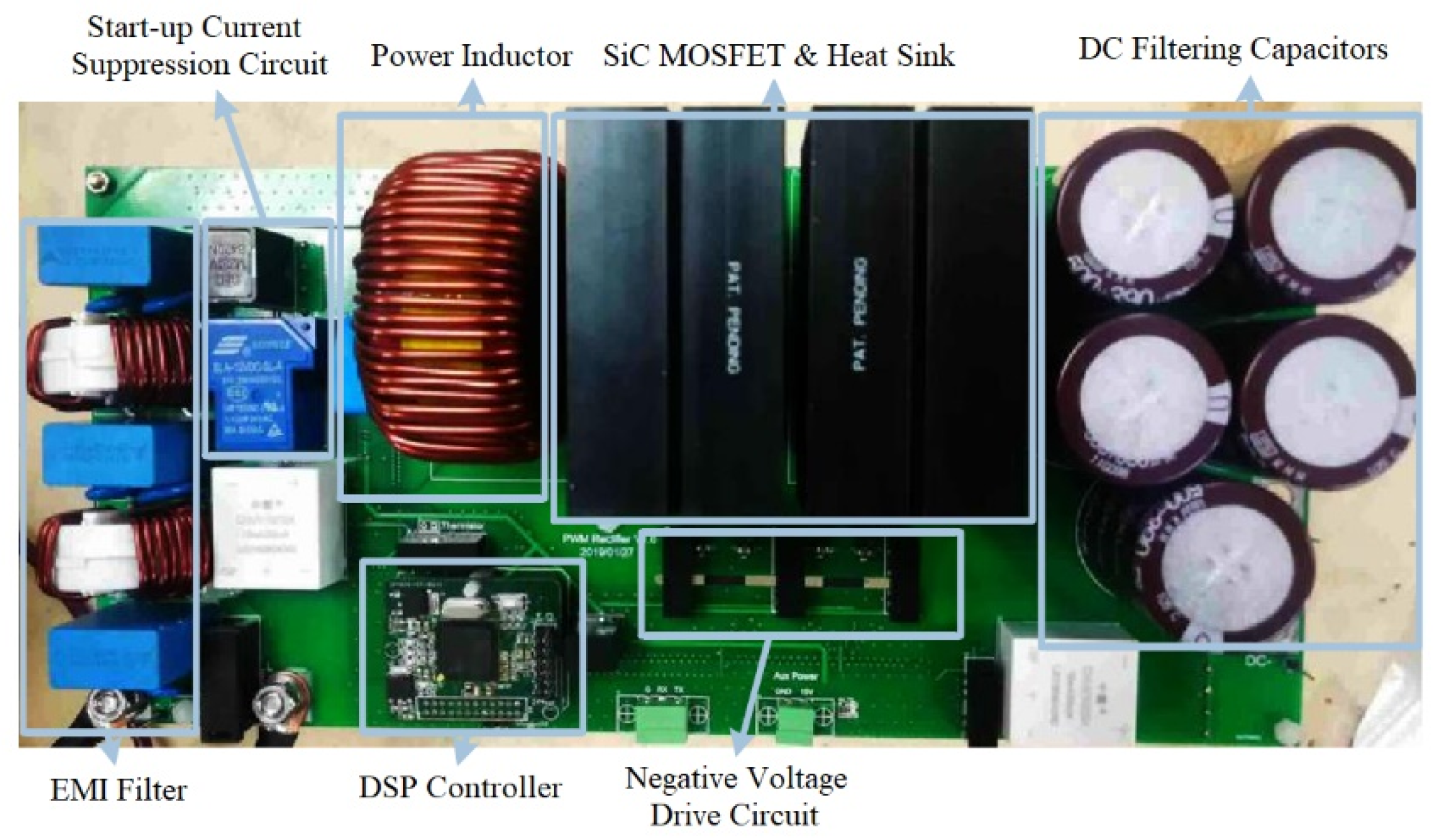
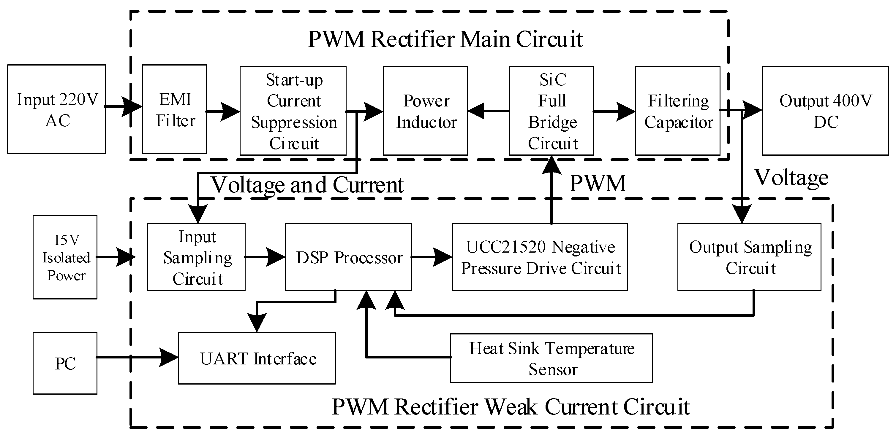
3. Circuit Component Analysis and Calculation

The role of the input inductor on the AC-side is to filter the switching current ripple and act as an energy storage inductor for the boost. The larger the inductance value is, the smaller the input current ripple becomes. Therefore, in the actual selection of the inductance, it is necessary to calculate the value range of the inductance according to the circuit parameters to meet the current ripple requirements and obtain better dynamic performance.

3.1. Analysis and Calculation of Inductance

To analyze the inductance, the switching period of the PWM rectifier is set at T with the duty cycle being D. It is set in one switching period, first mode I, followed by mode II. Taking the start time of a switching cycle as time 0, the equivalent transformation can be obtained
d i s d t = 1 L ( u a b u s )
Integrating both sides of the equation, we can get
i s ( t ) = 1 L ( u a b u s ) t + i s ( t 0 )
In mode I, the time t is [0, DT], and the input current is(t) can be calculated as
i s ( t ) = 1 L ( u o u S ) t + I min
where Imin is i(0). The rising value Δis+ of the input current in mode I is
i s + = i s ( D T ) i s ( 0 ) = 1 L ( u o u s ) D T
In Mode II, the time t is [DT, T], and the input current is(t) is
i S ( t ) = 1 L ( u o u s ) t + I max
where Imax is i(DT). The drop value Δis of the input current in Mode II is
i s = i s ( T ) i s ( D T ) = 1 L ( u o u s ) ( 1 D ) T
The rising value Δis+ of the ripple current is opposite to the negative sign of the falling value Δis, and the absolute value is the same as the value of Δis, namely
i s = i s + = i s
Then, T can be obtained as
T = D T + ( 1 D ) T = 2 L i s u o u 0 2 u s 2
and L can be calculated as
L = u o 2 u s 2 2 i s u o f
where f is the switching frequency. The optional minimum value of the inductance Lmn needs to be satisfied within the range of all us. The ripple current Δis can be adjusted within the requirements. When us = 0, the ripple current Δis is the largest. If the inductance L can meet the requirements at this time, ripple requirements can ensure that the ripple current Δis is within the range of the index requirements at any time. Based on this, we have
L min = u o 2 i s f
After determining the AC-side input current ripple size Δis, we can combine the switching frequency f and the DC-side output voltage uo to determine the minimum required inductance Lmn. It should not be smaller than the calculated Lmn.
The designed current ripple is 20% with a power of 3 kW when the input voltage is 220 V, and the effective value of the input current is 13 A. With the ripple current Δis = 2.6 A and the switching frequency of 100 kHz, we can get
L min = 400 2 × 2.6 × 100000 770   μ H

3.2. Analysis and Calculation of Capacitance

Considering that the input current can track the input voltage, high-order harmonics are introduced when the MOSFET is turned on and off and are filtered out. In practice, we have set the inductance value to be 820 μH.
The function of the DC-side output capacitor is to filter the switching voltage ripple. It can also absorb the rectified pulsating energy at the same time, supporting the DC-side voltage and the output voltage. The output capacitance value can be calculated based on the peak-to-peak value of the output DC voltage. When the capacitor absorbs the pulsating energy, the voltage across the capacitor will fluctuate on the final output.
The input voltage us and the input current is are expressed as
u s ( t ) = U S sin ( ω t )
i S ( t ) = I S sin ( ω t + φ )
where Us is the maximum value of the input voltage and Is is the maximum value of the input current. The input power can be calculated as
P i n = u s ( t ) i s ( t ) = U s I S 2 cos φ U S I S 2 cos ( 2 ω t φ )
The energy and power of the inductor are expressed as
E L = 1 2 L i S 2 ( t ) = 1 2 L I S 2 sin 2 ( ω t φ )
P L = ω L i S 2 ( t ) = ω L I S 2 sin ( ω t φ ) cos ( ω t φ )
The input power can be decomposed into constant power Po and fluctuating power Pr
P i n = P o + P r = U s I s 2 cos φ ( U s I s 2 cos ( 2 ω t φ ) + ω L I s 2 2 sin ( 2 ω t 2 φ ) )
where Po and Pr can be expressed as
P o = U S I S 2 cos φ
P r = ( U s I s 2 cos ( 2 ω t φ ) + ω L I s 2 2 sin ( 2 ω t 2 φ ) )
Po is the constant part of the output power. Pr is the fluctuating part of the output power, which is a power that changes periodically. The frequency of change is twice the power frequency. When the periodically fluctuating energy is applied to the capacitor, the voltage across the capacitor will also fluctuate. It will eventually appear as the ripple of the output voltage. The function of the output capacitor is to buffer and absorb the output voltage change caused by this part of the energy. Then, Pr can be transformed into
P r = U S 2 I s 2 4 cos 2 φ + ( ω L I s 2 2 U s I s 2 sin φ ) 2 × sin ( 2 ω t 2 φ + ψ )
where
ψ = arctan U S I S cos φ ω L I S 2 U S I S sin φ
Then, the wave energy can be calculated as
E r = 2 P r p e a k ω = 2 P o 2 + ( 2 ω L P o 2 U s 2 cos 2 φ P o sin φ cos φ ) 2 ω
When the output voltage is Uo, the energy stored on the support capacitor can be calculated as
E b 0 = 1 2 C b U o 2
where Cb is the capacitance of the support capacitor. When the voltage across the support capacitor rises at a value of ΔUo, the amount of change in the energy stored in the support capacitor ΔEb is
E b = E b 1 E b 0 = 1 2 C b ( U o + U o ) 2 1 2 C b U o 2 C b U o U o
The equivalent transformation can be obtained as
C b = E b U o U o
When the energy fluctuation stored in the support capacitor satisfies ΔEb = Er, we get
C b = E r U o U o = P o 2 + ( 2 ω L P o 2 U s 2 cos 2 φ P o ( sin φ cos φ ) ) 2 U o U o ω
Under the condition in which unity power factor φ = 0, we can get
C b = P o 2 + ( 2 ω L P o 2 U S 2 ) 2 U o U o ω
It can be seen that the capacitance of the output capacitor is mainly related to the output voltage and voltage ripple. In our design, the maximum output power Po = 3 kW; the output voltage is Uo; and the maximum voltage ripple is 3% or ΔUo = 12 V. Then, we can calculate Cb to be 1990 μF. Considering the relationship between a certain voltage margin and the size of the PWM rectifier board, five electrolytic capacitors with a withstand voltage of 390 μF of 500 V have been selected in parallel. The total capacitance value is Cb = 1950 μF.

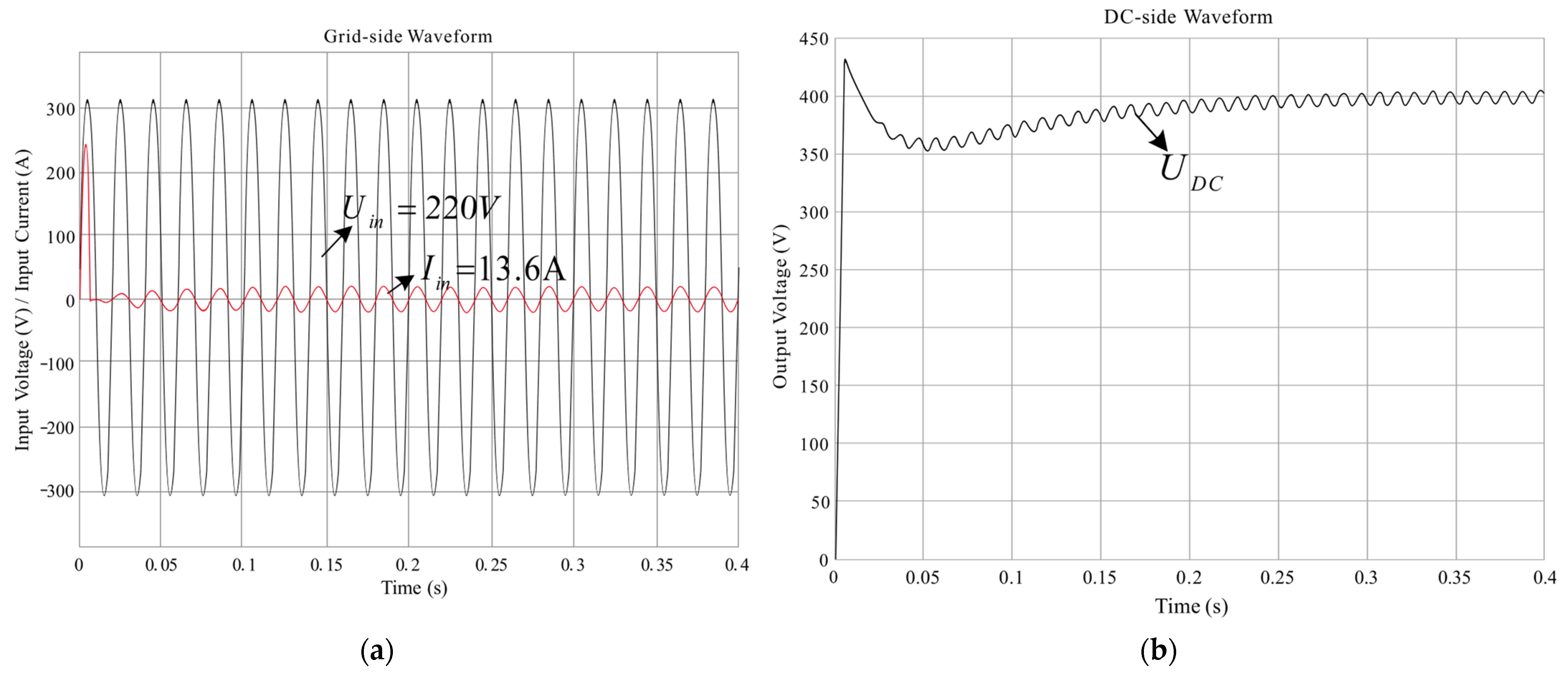
4. Simulation and Performance Comparison

The internal structure of the control module of the triangular wave comparison method is shown in Figure 7. The PI controller is used to adjust the output voltage. The input of the PI controller is the deviation between the expected output voltage and the actual output voltage. The output is the maximum value of the expected sinusoidal current. The output of the Product module is the expected input current that changes sinusoidally. After differentiating between the input current and the actual input current, the deviation value of the input current is obtained. After the deviation value is amplified by the Gain1 amplifier, it is sent to the PWM Generator module and modulated to generate 4 channels of PWM. The control signal is output to the full-bridge circuit in the main circuit as the final control signal.
Table 1 gives the simulation parameters. The waveforms of input voltage and current of the triangular wave comparison method are shown in Figure 8a. At 0.2 s, the rectifier has entered a steady-state, and the input current and input voltage waveforms are basically the same. The frequency is in the same phase, which achieves the purpose of power factor correction and harmonic current elimination. The DC-side voltage waveform is shown in Figure 8b. It can be seen that the output voltage rises rapidly to about 410 V. Then, due to integral action, the voltage value drops. Finally, the output voltage reaches around 400 V of the expected voltage in about 0.2 s. Then, the final output voltage tends to be stable.
The triangular wave current spectrum diagram is shown in Figure 9. The maximum harmonic frequency is limited to 1000 Hz, and the THD of the grid-side current is 3.53%.
The internal structure of the controller of the hysteresis current control method is shown in Figure 10. The structure of the voltage outer loop is the same as that of the triangular wave comparison method, but the current inner loop is different. In the hysteresis current control, the current inner loop sends the input current deviation to a hysteresis comparator relay and it uses the output of the hysteresis comparator as a switch tube control signal.
The switching frequency of the hysteresis current control is not fixed. In the simulation, the width of the current loop is set to 2 A. The waveform diagram of the hysteresis current control method is shown in Figure 11. The waveform diagram of the hysteresis current control method is basically the same as that of the triangular wave comparison method, except that the DC-side voltage waveform starts from 0 s, and the output voltage rises rapidly to 430 V. The initial voltage is higher than that of the triangle wave comparison method. The THD of the grid-side current is 6.62%, as shown in Figure 12.
The internal structure of the control module of the predictive current control method is shown in Figure 13. The PI control of the voltage outer loop is the same as that of the triangular wave comparison method. The current inner loop is constructed according to the predictive current control method. Through the operation, the duty cycle of the PWM is obtained, and then the rectifier is controlled.
The waveform diagram of the predictive current control method is shown in Figure 14. The dynamic response of the predictive current control method is better than the previous two traditional current control methods. The voltage reaches 390 V at 0 s due to the charging of the capacitor. The output voltages reached the expected value of 400 V and remained stable. The THD of the grid-side current is 1.86%, as shown in Figure 15.
Compared with the previous two control strategies, the THD of the predicted current control method is smaller. The total current harmonic distortion rate THD of the hysteresis current control is the highest. The current harmonic total distortion rate THD of the triangular wave comparison method and the predictive current control method are both relatively low. Among the three current control strategies, the predicted current control method has the smallest total current harmonic distortion rate THD. However, there is still room for improvement. When the value of the model inductance changes, the stability of the predictive current control method can be affected.
The simulation of the improved predictive current control strategy in the rotating coordinate system is shown in Figure 16.
The waveform diagram of the improved predictive current control method is shown in Figure 17. The THD of the grid-side current is 1.81%, as shown in Figure 18. Under the double closed-loop control, the output voltage can be stabilized near the required value, but the control effect of the predicted current and the improved predictive current control strategy is relatively better, and the latter can further simplify the calculation. In the initial stage, the start-up current is large. The reason for this is that due to the large capacitance of the latter stage, the energy in the capacitor is 0. The voltage on the capacitor cannot be abruptly changed, resulting in a large start-up current. When the voltage on the capacitor rises, the energy in the capacitor increases due to the relationship of Q = CU. Finally, the amplitude of the input current gradually tends to be stable. The waveform of the final steady-state input current is consistent with the input voltage in the same phase, achieving a unity power factor and eliminating current harmonics.
To simulate the situation when the inductance is not matched, we have replaced the 820 μH with 410 μH. Additionally, in order to simulate the results under the 110 V/60 Hz input condition, we have set the inductance at 400 μH and 200 μH in the matched and mismatched conditions. The performance comparison is shown in Table 2.
The algorithm is tested by simulation [35], and the robustness of the output voltage of the circuit is analyzed; the resulting data are shown in Table 3. When the input voltage is at 220 Vrms, 50 Hz, the expected output voltage is 400 V and the overshoot is 2.3%. When the output is 500 V, the overshoot is about 3.3%. Both outputs have a very fast rise and settling time. At the 110 Vrms, 60 Hz input condition with an output voltage of 400 V, the overshoot value is about 8.1%. At an output voltage of 500 V, the overshoot value is about 6.7%. Their rise and settling time are slightly longer than that of the 200 Vrms, 50 Hz input condition. Based on the results, the method still performs well.
In order to apply the algorithm on the embedded platform, its computational complexity needs to be considered when using the Simulink profiler [36,37]. After testing, the average time required for each invocation of the control function is 0.0000468 s. This preliminary complexity is suitable for DSP 28335, which is based on a 32-bit processor.

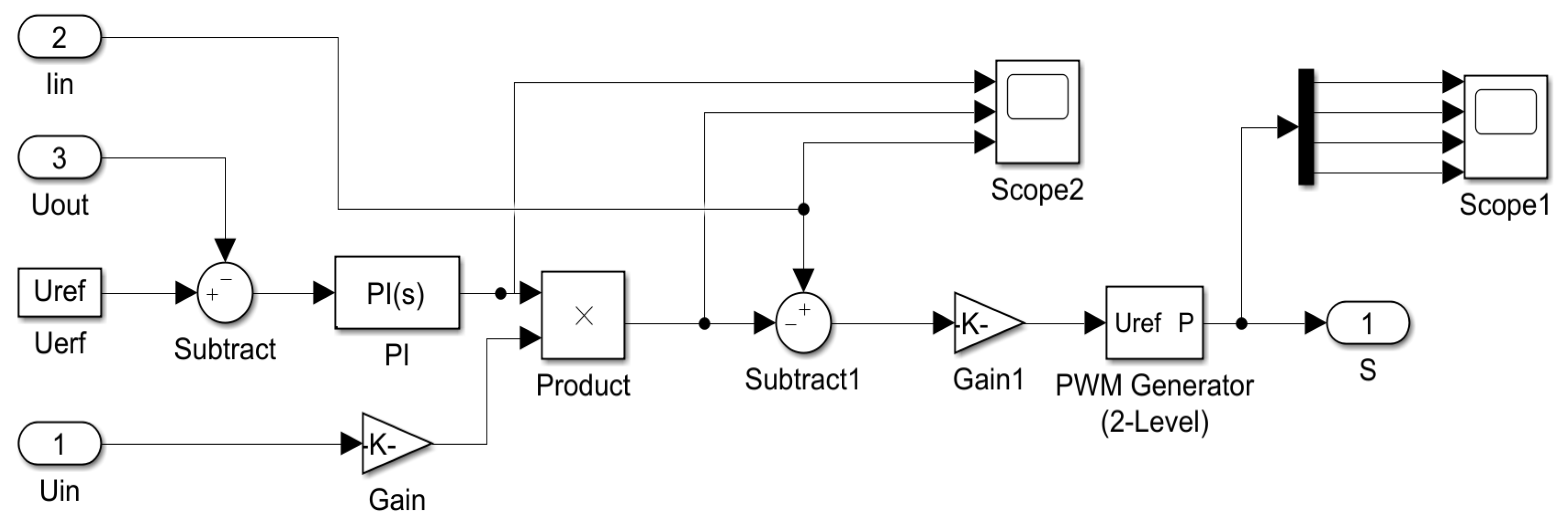
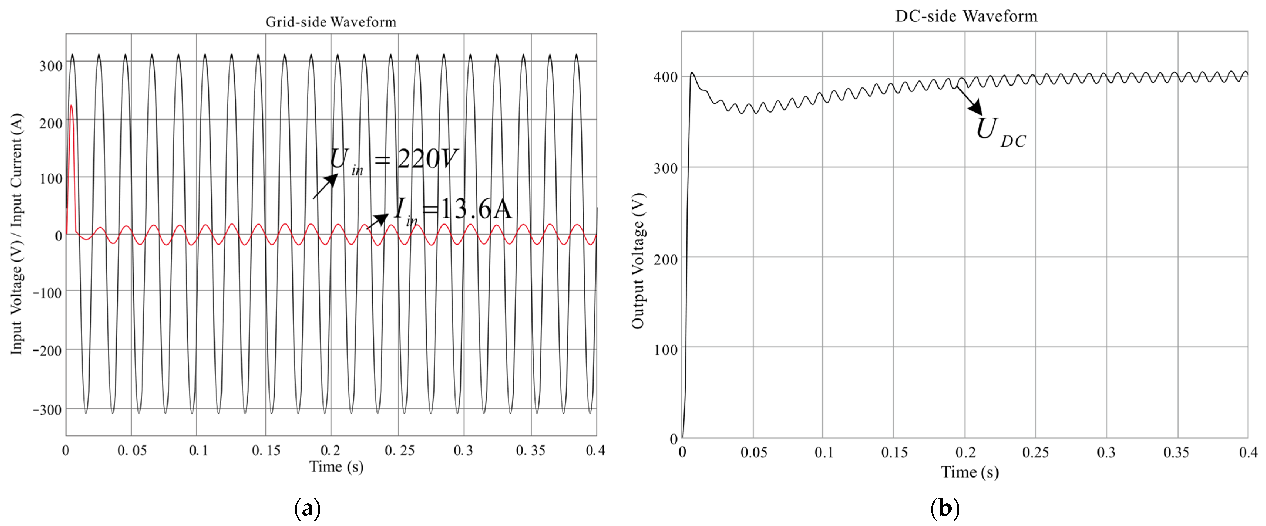
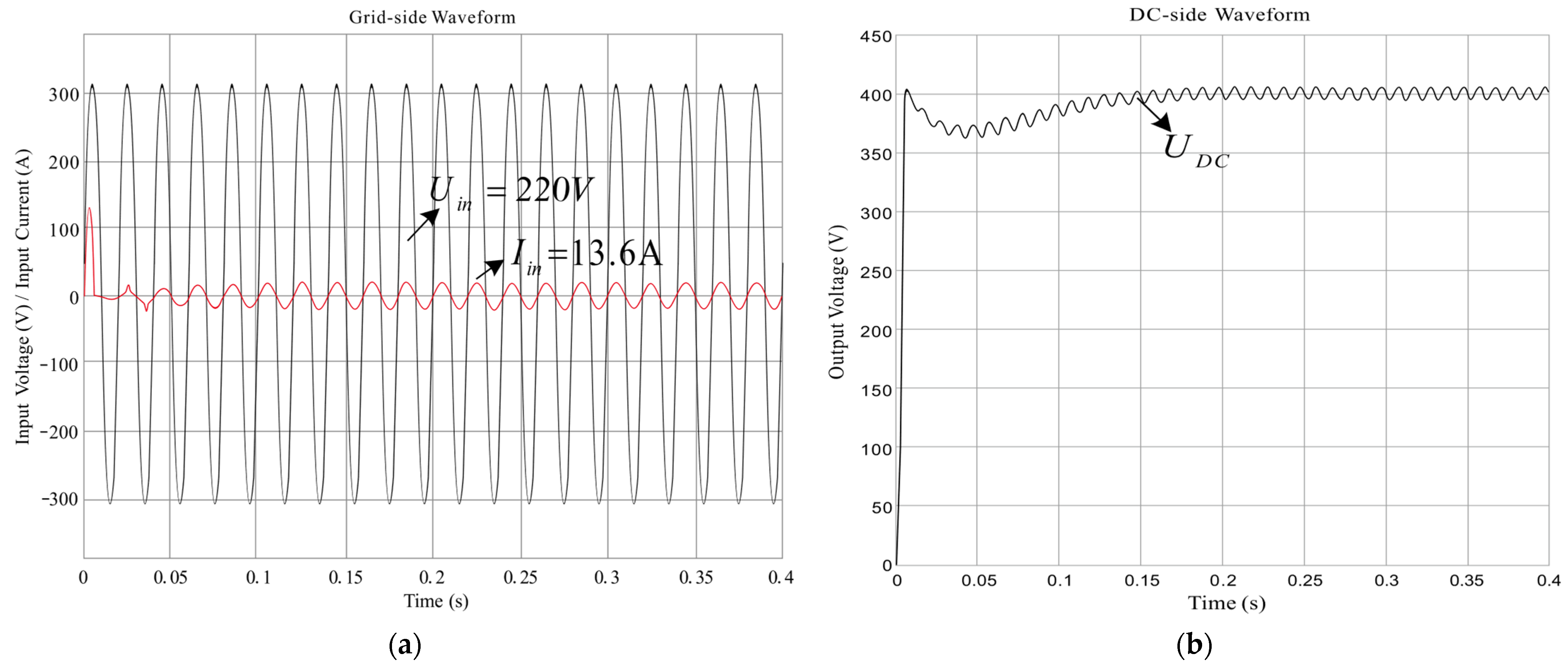
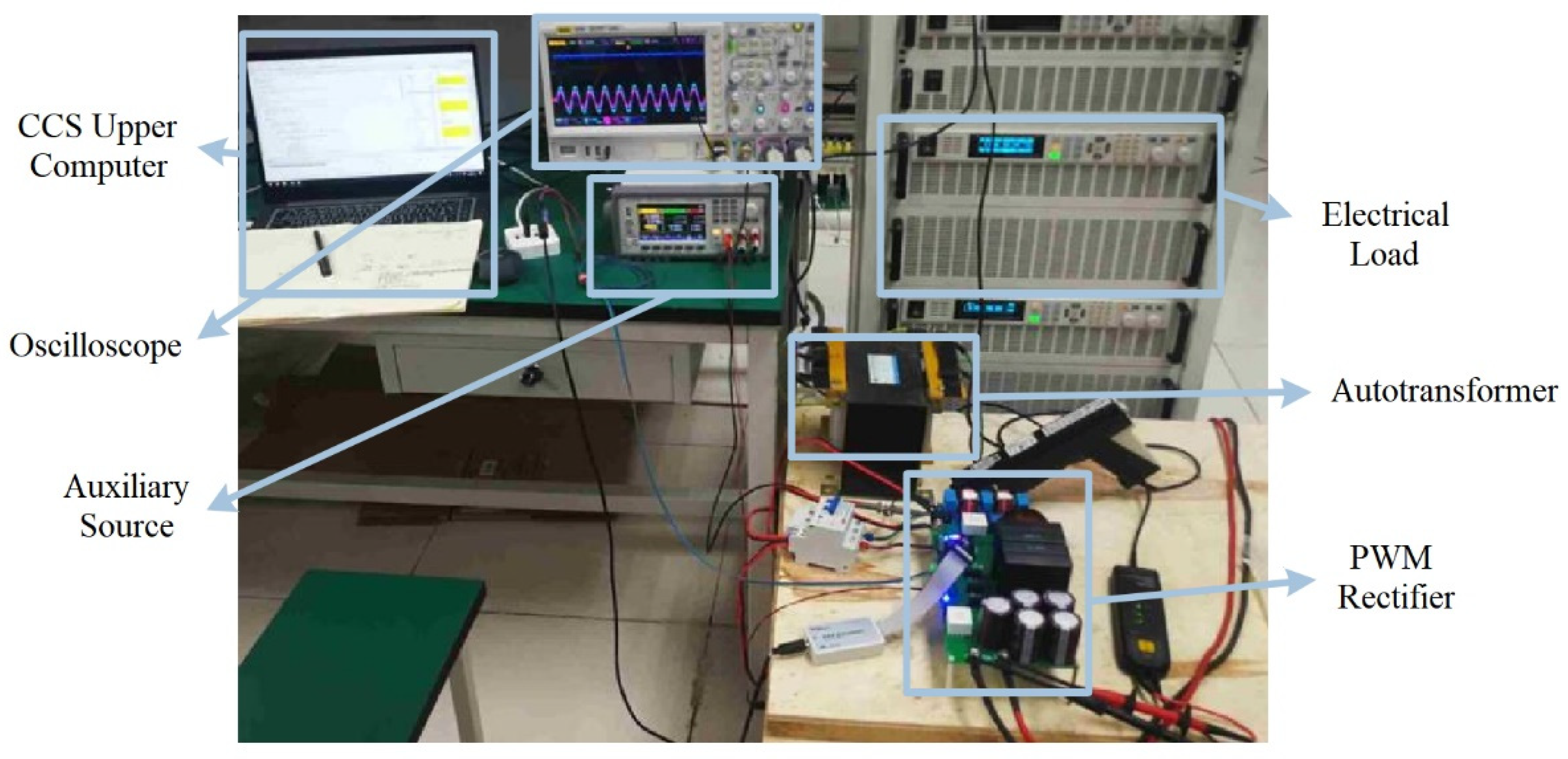
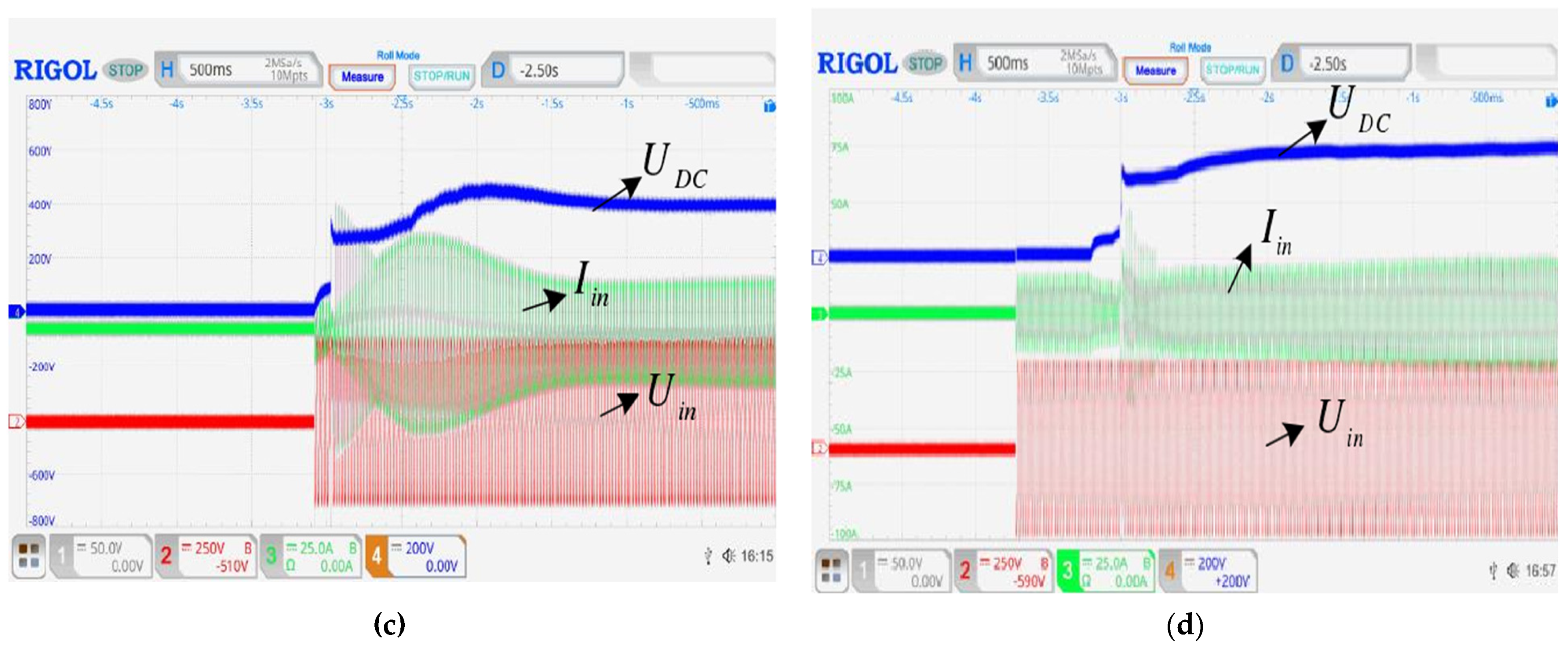
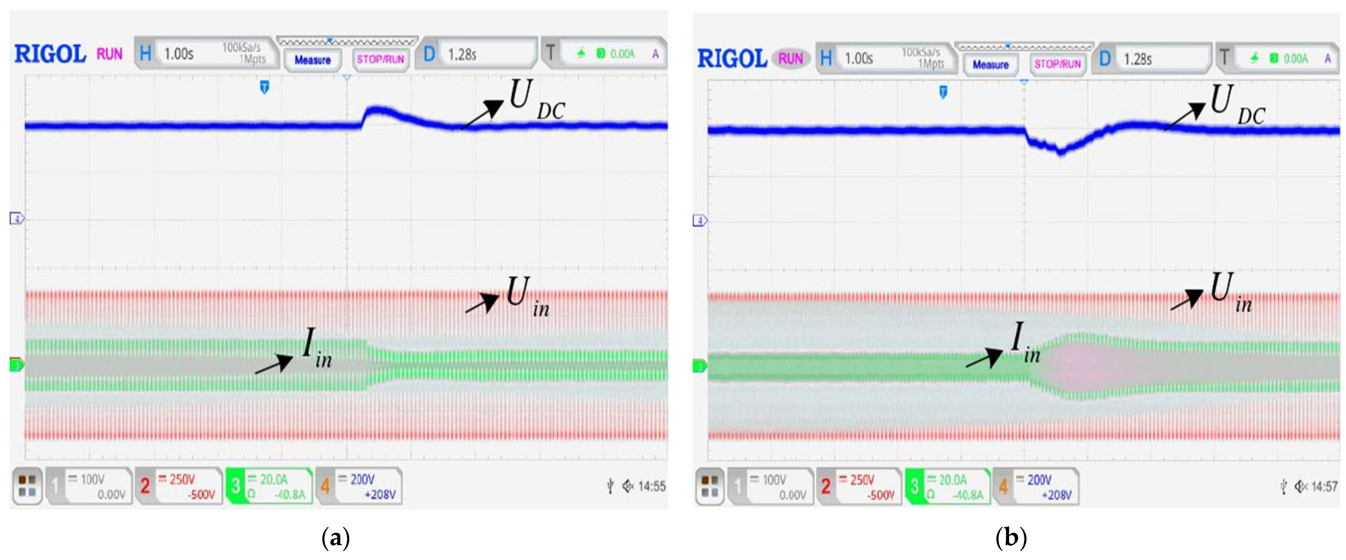
5. Experimental Results

The AC-side voltage of the single-phase PWM rectifier comes from the power grid. Its rated input voltage is 220 V with a frequency of 50 Hz. The voltage is in the form of a sine wave. However, due to the influence of electrical equipment on the power grid, the input voltage waveform has a certain fluctuating value in practical application. Therefore, when designing the hardware, it is necessary to consider the actual application situation. For the public power grid, it is necessary to include input filtering. The final hardware circuit photograph of the PWM rectifier is shown in Figure 19. It is mainly divided into the main circuit part of the PWM rectifier and the weak current part, of which, the main circuit part is mainly composed of an EMI filter and starting current suppression circuit, power inductor, full-bridge circuit, and DC filter capacitor to realize the conversion of input AC 220 VAC into output DC 400 VDC. The weak current part is mainly composed of the input acquisition circuit, DSP processor, negative pressure drive circuit, output acquisition circuit, and UART communication interface. The acquisition circuit is composed of input voltage and current acquisition, output voltage acquisition, and control signal output. The diagram of the rectifier structure is shown in Figure 20.

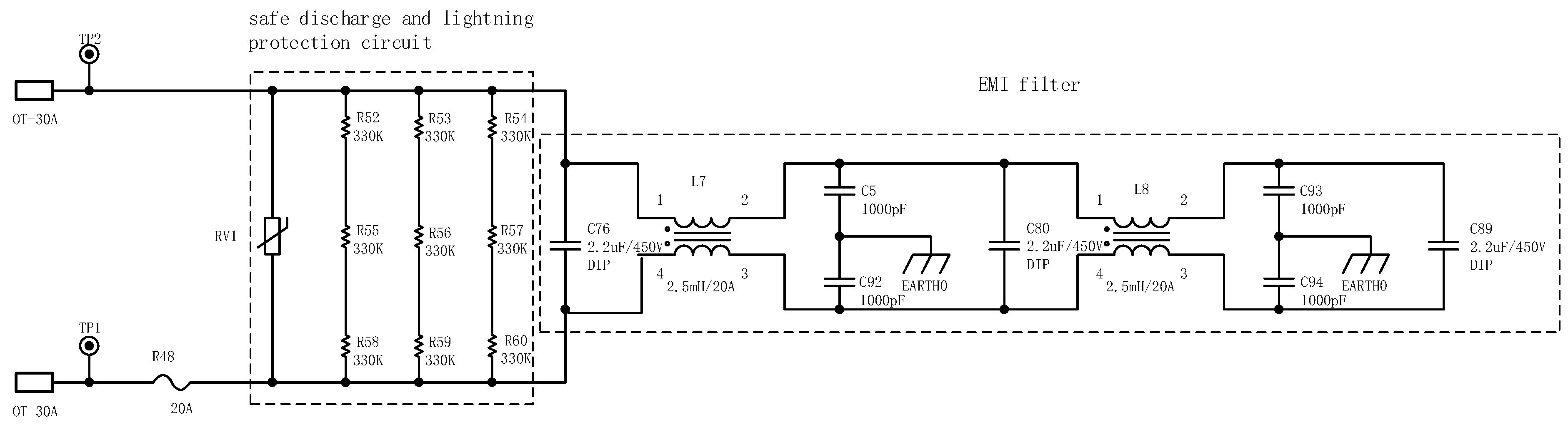
5.1. Design of Input Filtering for Harmonic Suppression

As shown in Figure 21, the EMI filter consists of two common mode inductors and four capacitors. The coils of the common mode inductors are all wound on the same iron core, and the number of turns and phases are the same but wound in opposite directions. Therefore, when the normal current signal passes through the common mode inductance, the currents generate opposite magnetic fields in the inductive coils wound in the same phase and cancel each other out. At this time, the normal current is mainly affected by the internal resistance of the common mode inductance. When a common-mode signal flows through the coil, since the direction of the common-mode current is the same, a magnetic field in the same direction is generated in the coil. This can increase the inductive reactance of the coil, producing a damping effect on the current, and attenuating the common-mode current. The capacitor is used to filter out the differential mode signal interference in the system.

5.2. Switch Tube Parameter Selection and Drive Circuit Design

In order to reduce the size of the grid-side inductance of the PWM rectifier, achieve high power density, improve control accuracy, and ensure the dynamic performance of the rectifier, a higher switching frequency is required. Considering the MOSFET’s withstand voltage, nominal current, on-resistance, switching time, diode recovery time, and other parameters, CREE’s C2M0080120D SiCMOSFET has been selected. It has a withstand voltage of 1200 V, a rated current of 36 A, an on-resistance of only 80 mΩ, and a turn-on delay of only 11 ns, which can meet our design requirements.
When designing the drive circuit, due to the layout and wiring of the circuit board, the gate of the MOSFET can appears. In order to reduce or avoid the misconnection and ringing of the bridge circuit caused by the high voltage and current change rate during turn-on, a fully isolated driver chip is used to design a negative voltage drive circuit. While optimizing the drive circuit parameters and circuit layout, a buffer circuit on the bridge circuit is set up. High-voltage ceramic capacitors are added near the MOSFET input to reduce ringing during switching. The specific negative voltage drive circuit is shown in Figure 22. The negative voltage is generated by the D3 and D5 Zener diodes. When the driver chip is turned off, the output voltage of the output pin connected to the gate of the MOSFET is zero. The MOSFET source voltage at the cathode of the Zener diode has the value of 5.1 V, and the MOSFET gate voltage Vgs is −5.1 V at this time. The power supply voltage is 15 V. The Vgs voltage is about 10 V when the MOSFET is turned on and the typical threshold voltage of the selected MOSFET is only 2.6 V, which meets the design requirements.
The driver chip selected is TI’s integrated driver chip UCC21520, which has a dual low-side, dual-high-side, or half-bridge driver with 5.7 kVRMS isolation. The chip also has a protection mechanism. When the dual-channel output is high at the same time, the output will be pulled down immediately to prevent a short-circuit and burnout of the protection circuit area.

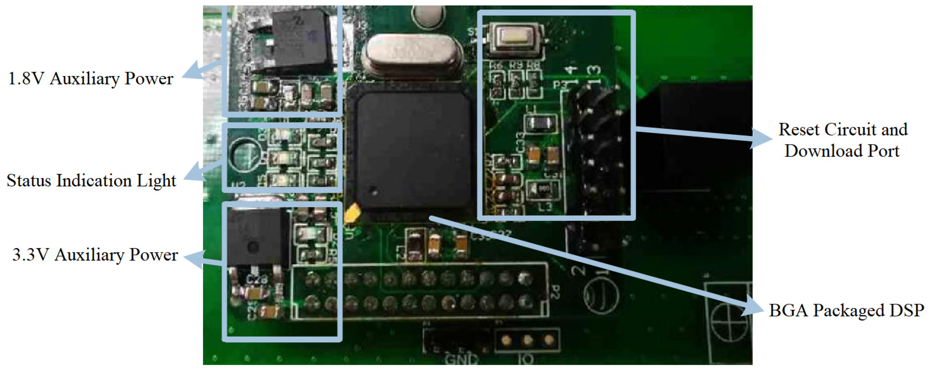
5.3. DSP Controller Selection and Control Board Design

This design adopts the digital signal processor of TI’s TMS320F28335 model. In order to ensure the hardware maintainability of the PWM rectifier board, the control board of the DSP and the PWM rectifier circuit are, respectively, modularized. The DSP is packaged with a plastic solder ball array. In the package, the array of solder balls is made on the bottom as the I/O of the circuit. Compared with the quad flat package, the package area can be greatly reduced and the density of the wiring layout can be increased. The 3.3 V and 1.8 V auxiliary power supply power the DSP chip, and the reset button and download port are added to the control board to facilitate debugging. The DSP control board is shown in Figure 23.

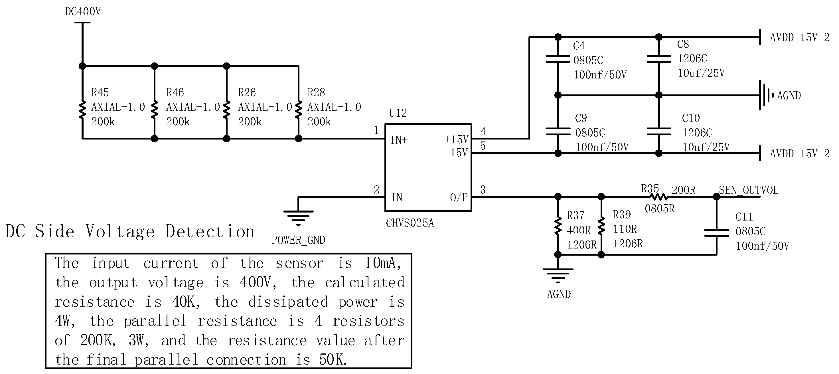
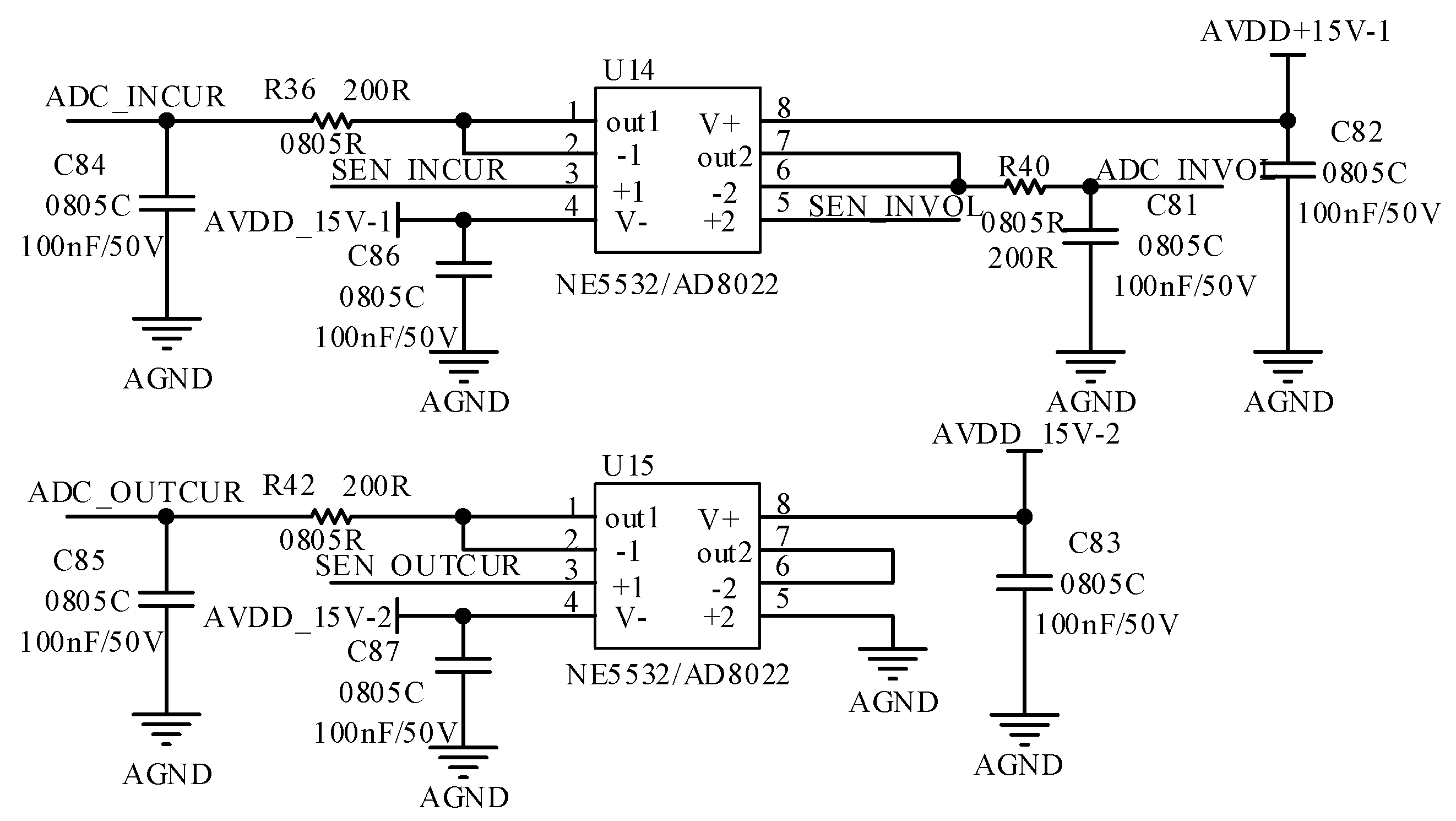
5.4. Design of Signal Sampling Circuit

No matter which current control strategy is used to form a double closed-loop control, it is necessary to detect the voltage and current at the grid-side and the output voltage at the DC-side. Its signal sampling circuit is shown in Figure 24 and Figure 25. Two detection voltage sensors are selected from the HVSS-025A series of the Zhonghuo Company with an isolation voltage of 2.5 kV and adopt a dual power supply which can directly collect the negative pressure on the AC side. Considering the resistance value of the common sense resistor and the redundancy design for the subsequent higher grid-side voltage, a 4 A 150 kΩ resistor with a dissipation power of 3 W is connected in parallel to support a total dissipation power of 12 W. The DC-side voltage is 400 V, and the calculated resistance is 40 kΩ. Considering the above redundancy, in the design, four 200 kΩ resistors with a dissipation power of 3 W are selected in parallel to support a total dissipation power of 12 W and a detection resistor with a resistance value of 50 kΩ. In order to facilitate debugging and reduce the interference of high-frequency harmonic noise, an RC low-pass filter is added to the output of the two detection circuits to filter out high-frequency noise.
The grid-side current detection circuit is shown in Figure 26 in which the AC-side current sensor adopts HCS-LTS-15A of CoreTech Company. The sensor is on the reference voltage of the output voltage of 2.5 V. According to the current flow, the current RMS value changes 15 A, and the sensor output voltage is increased or decreased by 0.625 V on the basis of the reference voltage. It also has a current accuracy of less than 0.7% and a response time of 1 μs, which meets the needs of this design.
At the output end of the above acquisition circuit, a voltage follower circuit is added. In this design, the op amp chip of TI company model NE5532 is used to build a voltage follower circuit. The positive pole of the op amp is connected to the input signal, and the negative pole and the output pin are shorted together as the output signal. This can improve the impedance of the input terminal and reduce the impedance of the output terminal to avoid the loss of the signal in the output resistance of the previous stage. A voltage follower is added here to play a buffering role to provide a high-quality signal input for the subsequent data acquisition of the external AD chip. The voltage follower circuit is shown in Figure 27. It is necessary to build a voltage follower with the input grounded to avoid introducing oscillation to other op amps.
Since the input voltage range of the internal AD channel of TMS320F28335 is 0~3 V, it is impossible to directly collect the signals of ±15 V output from the voltage sensor and ±5 V from the current sensor output. Adding an external conditioning circuit will further weaken the effective number of bits of the signal. Therefore, this design selects the ADC chip AD7324 of ANALOGDEVICES company which supports positive and negative voltage acquisition and has 4 AD channels. Each channel can select the range of input voltage through software programming, and the accuracy reaches 13 bits with a sampling rate is as high as 1 MHz. The external AD sampling circuit is shown in Figure 28, where channel 1 and channel 3 are the AC-side voltage and DC-side voltage acquisition channels. Since the output of the voltage sensor is high, the external AD chip channel 1 and channel 3 are set. The input voltage range is ±15 V. Channel 2 is a current sensor, and the output voltage is only 0~5 V. Therefore, the input voltage range of channel 2 of the external AD chip is set to ±5 V to improve the sampling accuracy.

5.5. Soft-Start Current-Limiting Circuit

When the output voltage is low, the current inner loop cannot control the current. The body diodes constitute an uncontrollable rectifier. The DC-side voltage of the uncontrollable rectifier is slightly lower than the grid-side voltage. In the uncontrollable rectification stage, the input current of the rectifier will have a very high current spike since the forward conduction time of the body diode accounts for a small proportion of the entire AC half-wave cycle. When the input voltage directly charges the support capacitor through the diode, the series equivalent resistance of the capacitor is small, resulting in a very large charging current and a current spike. Therefore, the circuit with the starting current suppression function is designed as shown in Figure 29. First, the rectifier current limiting resistor starts to work at startup. After a period of time, the relay bypass current limiting resistor is turned on, and the uncontrollable rectification is switched to PWM rectification to suppress the initial startup current.

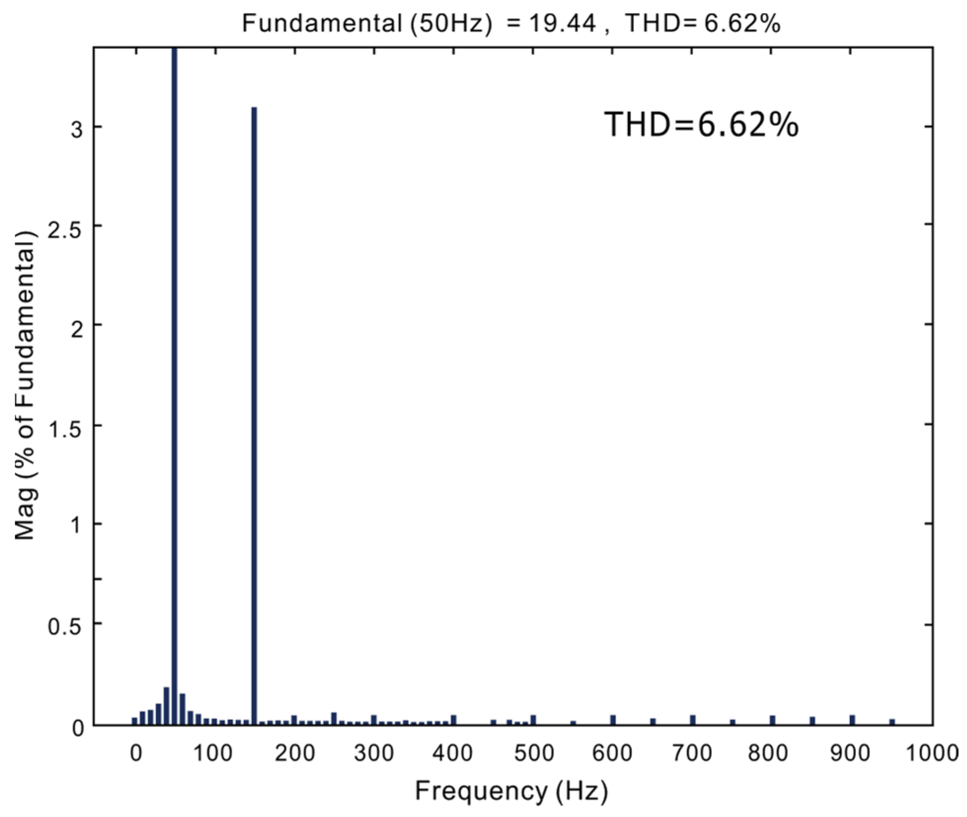
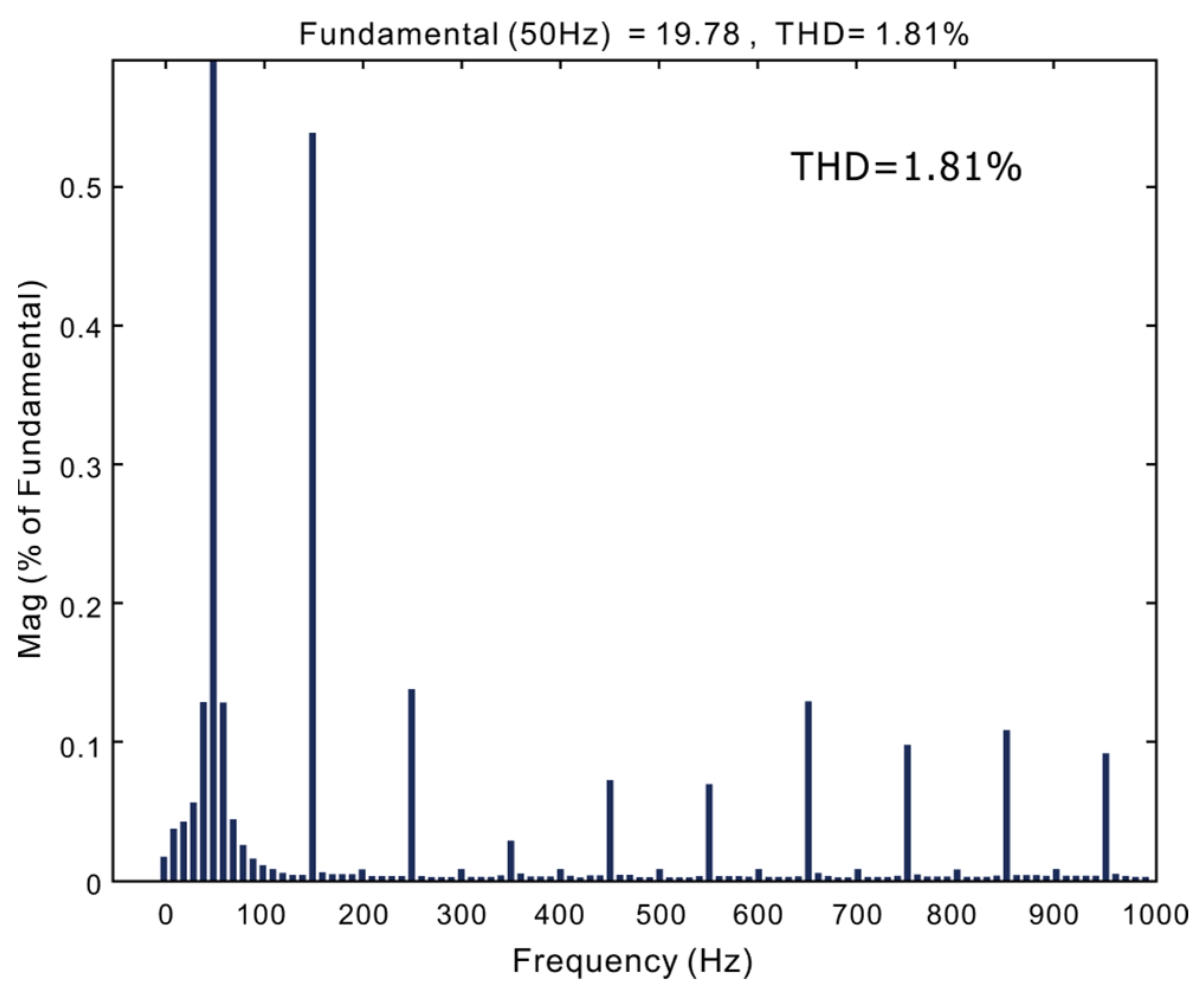
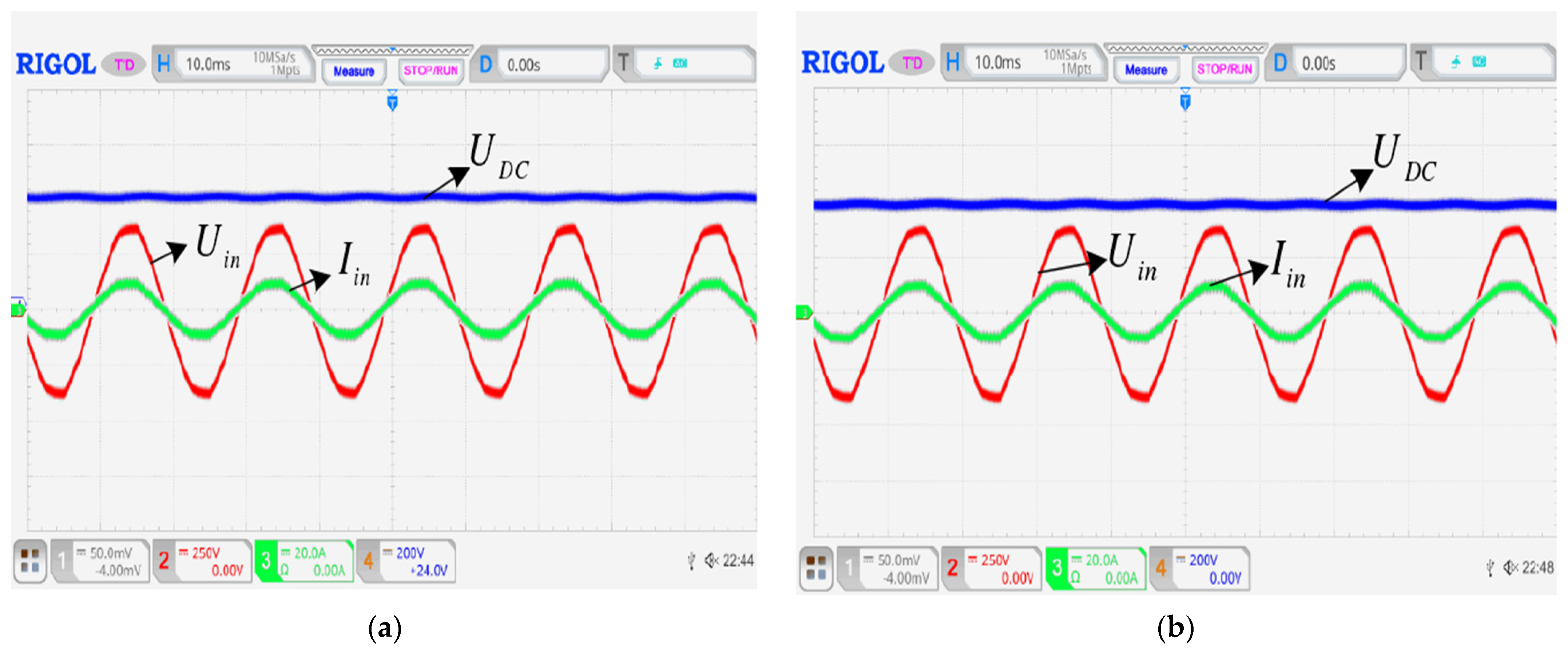
5.6. Experimental Results and Analysis

The double closed-loop control of a single-phase PWM rectifier is a more complicated control algorithm, and the control period of the voltage outer loop is longer than that of the current inner loop. When the grid-side current can dynamically track the grid-side voltage well, it can go back to fine-tune the voltage outer-loop parameters. When the load fluctuates greatly, the outer ring voltage can also be stabilized at the set value so as to prevent the DC-side voltage from being too high due to the load change.
According to the hardware circuit design, the experimental platform is built, as shown in Figure 30. The measurement setup consists of a strong electricity part and a weak electricity part. For the strong electricity part, the 50 Hz alternating current of the power grid is fed into the autotransformer to realize the adjustable input voltage. The output of the autotransformer is connected to the rectifier. The load adopts an electronic load whose power can be displayed. For the weak electricity part, the system uses an auxiliary power supply. The main control microcontroller processes the collected current and voltage data and controls the PWM output. The serial port communicates with the PC to observe the state of the rectifier. The voltages and current probes of the oscilloscope are placed at the input of the rectifier to test the input current and voltage waveform.
The measured steady waveforms are shown in Figure 31. The switching frequency of this design is 100 kHz, and the current control frequency is about 33 kHz. It can be seen that the current tracking voltage characteristics of the two algorithms are excellent. The THD of the traditional PI algorithm current obtained by FFT is 6.26%, and the THD of the improved predicted current algorithm current is 4.72%. During the test, the power grid is polluted by other high-power electrical equipment, and there are certain distortions and high-order harmonics. After passing through the EMI filter, part of the distortions and harmonics are attenuated. Therefore, they have little effect on the current control of the subsequent stage.
In order to prevent the PWM rectifier from generating an inrush current during startup, a thermistor with a positive temperature coefficient is added to suppress the peak current at the moment of startup. The no-load and full-load soft-start waveforms of the traditional PI algorithm and the improved predictive current control algorithm are shown in Figure 32. It can be seen that the traditional PI algorithm has obvious voltage fluctuations during the no-load soft-start. The maximum voltage is close to 500 V. With the full-load soft-start, the voltage is partially overshot, and the effect is not ideal. However, the no-load and full-load soft-start voltage waveforms of the improved predictive current control algorithm can quickly reach the expected value without serious voltage overshoot. It is overall better than the traditional PI algorithm.
During the test, due to the poor dynamic performance of the traditional PI algorithm, the DC-side voltage is likely to exceed the 500 V rated value of the electrolytic capacitor in the subsequent stage when the load changes sharply. The dynamic response test results are shown in Figure 33. When the load suddenly changes from 3 kW to 1.5 kW, the DC-side voltage changes to around 450 V; after about 0.8 s, the DC-side voltage stabilizes to 400 V. When the load suddenly changes from 1.5 kW to 3 kW, the DC-side voltage changes to about 350 V, and after about 1.2 s, the DC-side voltage stabilizes to 400 V again.
As shown in Table 4, the predictive current coordinate rotated control algorithm is used. A power analyzer is added to the input end to test the overall efficiency of the system at a VAC of 240 V and VDC of 400 V. The highest efficiency reaches 97.02%.
The comparison of simulated and measured results is shown in Table 5. In the test results, the power reaches 3.3 kW. The highest efficiency reaches 97%, and the highest PF reaches 0.9992 with a minimum THD of 3.57%. However, when with a light load at around 600 W, the THD reaches 6.39%. After analysis, it can be seen from the grid-side voltage waveform that this is caused by the fluctuation and instability of the grid voltage. Therefore, a certain distortion of the grid-side voltage waveform results and reduces the THD of the entire PWM rectifier.
In order to verify the rationality of this method, several other designs are compared, and the results shown in Table 6. It can be seen from the table that the proposed design method has a lower THD value and higher PF value.

6. Conclusions

This paper proposes a novel improved algorithm to control the voltage and current of PWM rectifiers. The design flow of the control algorithms of the current inner loops are simulated and measured. Then, the experimental results are compared on the built experimental platform which proves the correctness of the theoretical analysis and computer simulation. Finally, the efficiency of the whole machine is tested and analyzed for different loads, and a single-phase PWM rectifier with a high efficiency and unit power factor is realized. The proposed algorithm can be practically applied to the field of distributed energy storage in the home.

Author Contributions

Y.Z. (Yuying Zhu), Z.W., C.W., Y.Z. (Yuyu Zhu) and X.C. were involved in the simulation, measurement, writing, editing, and revising process of the present paper. All authors have read and agreed to the published version of the manuscript.

Funding

This work was supported by the Doctoral Foundation of Southwest University of Science and Technology (Nos. 19zx7156 and 20zx7121) and the Industry-University Cooperation Collaborative Education Project of the Ministry of Education, grant number 202101097010.

Data Availability Statement

The data presented in this study are available on request from the corresponding author.

Acknowledgments

We would like to thank the reviewers for their valuable questions and suggestions.

Conflicts of Interest

The authors declare no conflict of interest.

References

  1. Mao, J.; Hong, D.; Ren, R.; Li, X. The Effect of Marine Power Generation Technology on the Evolution of Energy Demand for New Energy Vehicles. J. Coast. Res. 2020, 103, 1006. [Google Scholar] [CrossRef]
  2. Dini, P.; Saponara, S. Model-Based Design of an Improved Electric Drive Controller for High-Precision Applications Based on Feedback Linearization Technique. Electronics 2021, 10, 2954. [Google Scholar] [CrossRef]
  3. Benedetti, D.; Agnelli, J.; Gagliardi, A.; Dini, P.; Saponara, S. Design of an Off-Grid Photovoltaic Carport for a Full Electric Vehicle Recharging. In Proceedings of the 2020 IEEE International Conference on Environment and Electrical Engineering and 2020 IEEE Industrial and Commercial Power Systems Europe (EEEIC/I&CPS Europe), Madrid, Spain, 9–12 June 2020; pp. 1–6. [Google Scholar]
  4. Dini, P.; Saponara, S. Analysis, design, and comparison of machine-learning techniques for networking intrusion detection. Designs 2021, 5, 9. [Google Scholar] [CrossRef]
  5. Qian, Y.; Jiang, C.; Chen, C. Research on the Effects of New Energy Power Generation on Power System. In Proceedings of the International Conference on Logistics Engineering, Management and Computer Science (LEMCS 2015), Shenyang, China, 29–31 July 2015; pp. 1146–1150. [Google Scholar]
  6. Conlon, T.; Waite, M.; Modi, V. Assessing new transmission and energy storage in achieving increasing renewable generation targets in a regional grid. Appl. Energy 2019, 250, 1085–1098. [Google Scholar] [CrossRef]
  7. Cosimi, F.; Dini, P.; Giannetti, S.; Petrelli, M.; Saponara, S. Analysis and Design of a Non-linear MPC Algorithm for Vehicle Trajectory Tracking and Obstacle Avoidance. In Proceedings of the International Conference on Applications in Electronics Pervading Industry, Environment and Society, Pisa, Italy, 21–22 September 2020; pp. 229–234. [Google Scholar]
  8. Bernardeschi, C.; Dini, P.; Domenici, A.; Saponara, S. Co-Simulation and Verification of a Non-Linear Control System for Cogging Torque Reduction in Brushless Motors. In Proceedings of the International Conference on Software Engineering and Formal Methods, Oslo, Norway, 16–20 September 2019; pp. 3–19. [Google Scholar]
  9. Li, Y.; Shu, Z.; Zhu, Q. Application of Wave Power Generation in New Energy. J. Coast. Res. 2020, 105, 89–92. [Google Scholar] [CrossRef]
  10. Kim, S.H.; Baek, S.C.; Choi, K.B.; Park, S.J. Design and installation of 500-kW floating photovoltaic structures using high-durability steel. Energies 2020, 13, 4996. [Google Scholar] [CrossRef]
  11. Wu, Z.; Chang, Y.; Li, Q.; Cai, R. A Novel Method for Tunnel Digital Twin Construction and Virtual-Real Fusion Application. Electronics 2022, 11, 1413. [Google Scholar] [CrossRef]
  12. Benedetti, D.; Agnelli, J.; Gagliardi, A.; Dini, P.; Saponara, S. Design of a Digital Dashboard on Low-Cost Embedded Platform in a Fully Electric Vehicle. In Proceedings of the 2020 IEEE International Conference on Environment and Electrical Engineering and 2020 IEEE Industrial and Commercial Power Systems Europe (EEEIC/I&CPS Europe), Madrid, Spain, 9–12 June 2020; pp. 1–5. [Google Scholar]
  13. Coteli, R.; Acikgoz, H.; Ucar, F.; Dandil, B. Design and implementation of Type-2 fuzzy neural system controller for PWM rectifiers. Int. J. Hydrog. Energy 2017, 42, 20759–20771. [Google Scholar] [CrossRef]
  14. Park, J.H.; Lee, J.S.; Lee, K.B. Sinusoidal Harmonic Voltage Injection PWM Method for Vienna Rectifier with an LCL-filter. IEEE Trans. Power Electron. 2020, 36, 2875–2888. [Google Scholar] [CrossRef]
  15. Pierpaolo, D.; Saponara, S. Control System Design for Cogging Torque Reduction Based on Sensor-Less Architecture. In Proceedings of the International Conference on Applications in Electronics Pervading Industry, Environment and Society, Pisa, Italy, 11–13 September 2019; pp. 309–321. [Google Scholar]
  16. Li, Q.; Jiang, D. Variable Switching Frequency PWM Strategy of Two-Level Rectifier for DC-link Voltage Ripple Control. IEEE Trans. Power Electron. 2017, 33, 7193–7202. [Google Scholar] [CrossRef]
  17. Vanco, W.E.; Silva, F.B.; Monteiro, J.; Oliveira, J.M.D.; Alves, A.C.; Júnior, C.A. Analysis of the oscillations caused by harmonic pollution in isolated synchronous generators. Electr. Power Syst. Res. 2017, 147, 280–287. [Google Scholar] [CrossRef]
  18. Xu, H.; Shao, Z.; Chen, F. Data-Driven Compartmental Modeling Method for Harmonic Analysis—A Study of the Electric Arc Furnace. Energies 2019, 12, 4378. [Google Scholar] [CrossRef] [Green Version]
  19. Alabduljabbar, A.A.; Smiai, M. A Methodology for Designing Low Power Factor Penalties in Distribution Networks. In Proceedings of the 2015 IEEE Power & Energy Society General Meeting, Denver, CO, USA, 26–30 July 2015; pp. 1–5. [Google Scholar]
  20. Dini, P.; Saponara, S. Design of an observer-based architecture and non-linear control algorithm for cogging torque reduction in synchronous motors. Energies 2020, 13, 2077. [Google Scholar] [CrossRef]
  21. Hou, M.K.; Chen, C.H.; Cheng, M.Y. Design and analysis of a single-phase low-frequency active power factor correction circuit: A symmetric trapezoidal current waveform approach. Electr. Eng. 2016, 98, 257–270. [Google Scholar] [CrossRef]
  22. Liu, M.; Zhao, P.; Wu, T.; Parhi, K.K.; Zeng, X.; Chen, Y. A low-power twiddle factor addressing architecture for split-radix FFT processor. Microelectron. J. 2021, 117, 105276. [Google Scholar] [CrossRef]
  23. Xu, D.P.; Jiang, Y.W.; Kwon, J.H.; Hwang, S.M. Analysis of the Effects of Electromagnetic Circuit Variables on Sound Pressure Level and Total Harmonic Distortion in a Balanced Armature Receiver. IEEE Trans. Magn. 2017, 53, 1–4. [Google Scholar] [CrossRef]
  24. Dini, P.; Saponara, S. Cogging torque reduction in brushless motors by a nonlinear control technique. Energies 2019, 12, 2224. [Google Scholar] [CrossRef] [Green Version]
  25. Dutta, A.; Koley, K.; Saha, S.K.; Sarkar, C.K. Impact of temperature on linearity and harmonic distortion characteristics of underlapped FinFET. Microelectron. Reliab. 2016, 61, 99–105. [Google Scholar] [CrossRef]
  26. Akbari, A.; Danesh, M.; Khalili, K. A method based on spindle motor current harmonic distortion measurements for tool wear monitoring. J. Braz. Soc. Mech. Sci. Eng. 2017, 39, 5049–5055. [Google Scholar] [CrossRef]
  27. Barbie, E.; Rabinovici, R.; Kuperman, A. Closed-Form Analytic Expression of Total Harmonic Distortion in Single-Phase Multilevel Inverters with Staircase Modulation. IEEE Trans. Ind. Electron. 2019, 67, 5213–5216. [Google Scholar] [CrossRef]
  28. Hu, H.; He, Z.; Gao, S. Harmonic distortion degradation and filter optimization based on sensitivity studies with considering resonance issue. IEEJ Trans. Electr. Electron. Eng. 2015, 10, 512–520. [Google Scholar] [CrossRef]
  29. Wang, R.; Li, C.; Han, X.; Liu, C. Carrier-based PWM modulation strategy for dual-output two-stage matrix converter. IET Power Electron. 2019, 12, 2135–2145. [Google Scholar] [CrossRef]
  30. Ranjan, R.K.; Mazumdar, K.; Pal, R.; Chandra, S. Generation of square and triangular wave with independently controllable frequency and amplitude using OTAs only and its application in PWM. Analog. Integr. Circuits Signal Processing 2017, 92, 1–13. [Google Scholar] [CrossRef]
  31. Liu, B.; Zha, Y.; Zhang, T.; Chen, S. Triple-state hysteresis direct power control for three phase PWM rectifier. In Proceedings of the 2015 IEEE International Conference on Mechatronics and Automation (ICMA), Beijing, China, 2–5 August 2015; pp. 783–789. [Google Scholar]
  32. Li, Y.; Zhao, H. A Space Vector Switching Pattern Hysteresis Control Strategy in VIENNA Rectifier. IEEE Access 2020, 8, 60142–60151. [Google Scholar] [CrossRef]
  33. Liu, Y.C.; Ge, X.; Tang, Q.; Deng, Z.; Gou, B. Model predictive current control for four-switch three-phase rectifiers in balanced grids. Electron. Lett. 2016, 53, 44–46. [Google Scholar] [CrossRef]
  34. Zhang, Y.; Liu, X.; Li, B.; Liu, J. Robust predictive current control of PWM rectifier under unbalanced and distorted network. IET Power Electron. 2021, 14, 797–806. [Google Scholar] [CrossRef]
  35. Dini, P.; Saponara, S. Electro-Thermal Model-Based Design of Bidirectional On-Board Chargers in Hybrid and Full Electric Vehicles. Electronics 2021, 11, 112. [Google Scholar] [CrossRef]
  36. Dini, P.; Saponara, S. Design of adaptive controller exploiting learning concepts applied to a BLDC-based drive system. Energies 2020, 13, 2512. [Google Scholar] [CrossRef]
  37. Bernardeschi, C.; Dini, P.; Domenici, A.; Palmieri, M.; Saponara, S. Formal verification and co-simulation in the design of a synchronous motor control algorithm. Energies 2020, 13, 4057. [Google Scholar] [CrossRef]
  38. Renjini, G. Comparison between Peak and Average Current Mode Control of Improved Bridgeless Flyback Rectifier with Bidirectional Switch. In Proceedings of the 2015 International Conference on Technological Advancements in Power and Energy (TAP Energy), Vallikavu, India, 24–26 June 2015; pp. 254–259. [Google Scholar]
  39. Xiao, D.; Alam, K.S.; Akter, M.P.; Shakib, S.S.I.; Zhang, D.; Rahman, M.F. Modulated model predictive control for four-leg inverters with online duty ratio optimization. IEEE Trans. Ind. Appl. 2020, 56, 3114–3124. [Google Scholar] [CrossRef]
  40. Mei, J.; Miao, H.; Huang, C.; Xu, Y.; Ma, T.; Hu, Q.; Chen, W. Hybrid one-cycle control scheme for fault-tolerant modular multilevel rectifiers. Int. J. Electron. 2017, 104, 1483–1499. [Google Scholar] [CrossRef]
  41. Nguyen-Van, T.; Abe, R.; Tanaka, K. Digital adaptive hysteresis current control for multi-functional inverters. Energies 2018, 11, 2422. [Google Scholar] [CrossRef] [Green Version]
  42. Cheng, C.A.; Chang, E.C.; Tseng, C.H.; Chung, T.Y. A single-stage LED tube lamp driver with power-factor corrections and soft switching for energy-saving indoor lighting applications. Appl. Sci. 2017, 7, 115. [Google Scholar] [CrossRef] [Green Version]
  43. Zhao, C.; Zhang, J.; Wu, X. An Improved Variable On-Time Control Strategy for a CRM Flyback PFC Converter. IEEE Trans. Power Electron. 2016, 32, 915–919. [Google Scholar] [CrossRef]
  44. Malekanehrad, M.; Adib, E. Bridgeless Single-Phase Step-Down PFC Converter. IET Power Electron. 2016, 9, 2631–2636. [Google Scholar] [CrossRef]
  45. Narasimhulu, V.; Kumar, D.V.A.; Babu, C.S. Computational intelligence based control of cascaded H-bridge multilevel inverter for shunt active power filter application. J. Ambient. Intell. Humaniz. Comput. 2020, 11, 1–9. [Google Scholar] [CrossRef]
Figure 1. The block diagram of a hybrid power generation system.
Electronics 11 01435 g001
Figure 2. The Structure of a PWM rectifier.
Electronics 11 01435 g002
Figure 3. The conversion of three-phased and two-phased coordinate systems.
Electronics 11 01435 g003
Figure 4. The transformation of virtual vector and α-β static coordinate system.
Electronics 11 01435 g004
Figure 5. The control block diagram under the rotating coordinate system.
Electronics 11 01435 g005
Figure 6. Block diagram of the closed-loop feedback control system.
Electronics 11 01435 g006
Figure 7. Control structure block diagram of the triangular wave comparison method.
Electronics 11 01435 g007
Figure 8. Triangle wave comparison method input and output waveforms (a) Grid-side voltage and current waveform (b) DC-side voltage waveform.
Electronics 11 01435 g008
Figure 9. Triangular wave current spectrum diagram.
Electronics 11 01435 g009
Figure 10. Structure block diagram of hysteresis current control method.
Electronics 11 01435 g010
Figure 11. Hysteresis current control method waveform diagram (a) Grid-side voltage and current waveform (b) DC-side voltage waveform.
Electronics 11 01435 g011
Figure 12. Hysteresis current control method grid-side current spectrum.
Electronics 11 01435 g012
Figure 13. Structure block diagram of predictive current control method.
Electronics 11 01435 g013
Figure 14. Predictive current control method waveform (a) Grid-side voltage and current waveform (b) DC-side voltage waveform.
Electronics 11 01435 g014
Figure 15. Predictive current control method grid-side current spectrum.
Electronics 11 01435 g015
Figure 16. Structure block diagram of improved predictive current control method.
Electronics 11 01435 g016
Figure 17. Waveform diagram of improved predictive current control method (a) Grid-side voltage and current waveform (b) DC-side voltage waveform.
Electronics 11 01435 g017
Figure 18. Grid-side current spectrum diagram of improved predictive current control method.
Electronics 11 01435 g018
Figure 19. The photograph of the single-phase PWM rectifier hardware circuit.
Electronics 11 01435 g019
Figure 20. The diagram of the rectifier structure.
Electronics 11 01435 g020
Figure 21. EMI filter design.
Electronics 11 01435 g021
Figure 22. Negative pressure drive circuit.
Electronics 11 01435 g022
Figure 23. DSP control board.
Electronics 11 01435 g023
Figure 24. Input voltage detection circuit.
Electronics 11 01435 g024
Figure 25. Output voltage detection circuit.
Electronics 11 01435 g025
Figure 26. Grid-side current detection circuit.
Electronics 11 01435 g026
Figure 27. Voltage follower circuit.
Electronics 11 01435 g027
Figure 28. External AD sampling power.
Electronics 11 01435 g028
Figure 29. Design of Control Algorithm for Starting Current Suppression Circuit.
Electronics 11 01435 g029
Figure 30. The photograph experimental platform.
Electronics 11 01435 g030
Figure 31. Steady-state waveforms of grid-side voltage, current, and DC-side voltage (a) Traditional PI algorithm (b) Improved Predictive Current Control Algorithm.
Electronics 11 01435 g031
Figure 32. Soft-Start Waveforms of the Traditional PI Algorithm and Improved Predicted Current Algorithm: (a) Traditional PI algorithm empty carrier waveform, (b) Improved Predictive Current Control Algorithm for Empty Carrier Waveform, (c) Traditional PI algorithm full carrier waveform, and (d) Improved Predictive Current Control Algorithm Full-Load Waveform.
Electronics 11 01435 g032aElectronics 11 01435 g032b
Figure 33. Dynamic Response Waveform of Improved Predictive Current Algorithm (a) load from 3 kW to 1.5 kW (b) load from 1.5 kW to 3kW.
Electronics 11 01435 g033
Table 1. Circuit parameters and requirements of our design.
Circuit ParametersValue
Grid-side Voltage Uin220 VAC/50 Hz
DC-side Voltage UDC400 VDC
Grid-side Inductor L820 μH
DC-side Capacitor C2000 μF
Circuit Equivalent Resistor R0.2 Ω
Switching Frequency F100 kHz
Rated Output Power PDC3000 W
Table 2. Grid-side current THD under different current control strategies.
Control AlgorithmTHD at Grid-Side L of 820 μHTHD at Grid-Side L of 410 μH
Triangle wave method3.53%4.16%
Hysteresis current method6.62%8.76%
Predictive current method1.86%5.26%
Proposed method1.81%2.57%
Table 3. Simulation results of different operating conditions.
Operating ConditiontrTs,5%Omaxe
220 Vrms and 50 Hz, 400 V0.02 s0.08 s2.3%<1%
110 Vrms and 60 Hz, 400 V0.11 s0.24 s8.1%<1%
220 Vrms and 50 Hz, 500 V0.02 s0.09 s3.3%<1%
110 Vrms and 60 Hz, 500 V0.14 s0.30 s6.7%<1%
Table 4. Measured specifications and values.
VAC (V)IAC (A)PAC (W)PFVDC (V)IDC (A)PDC (W)Efficiency (%)THD
240.12.884678.40.9916399.881.667666.596.25%6.39%
240.055.1791243.50.9965399.893.0041201.396.61%5.06%
240.07.8191876.50.9986399.934.541815.796.76%4.72%
239.7810.4302500.80.9987400.146.0522421.596.83%4.21%
239.5412.9893111.50.999400.047.5383015.496.91%3.92%
239.4114.1933398.00.9992400.028.2413296.797.02%3.57%
Table 5. Comparison of main design specifications.
ParametersSimulated ResultsMeasured Results
Input Voltage85~240 VAC110~240 VAC
Frequency47~63 Hz50 Hz
THD1.81%3.57%
Power Factor0.99970.9992
Output Voltage380~420 VDC380~420 VDC
Output Voltage Ripple15.2 V18 V
Maximum Power3 kW3296 W
Peak Efficiency98.1%97.02%
Table 6. Performance comparison.
MethodInput VoltageFrequencyTHDPower FactorOutput
Voltage
Output
Voltage Ripple
Maximum
Power
CMC [38]90~140 VAC35 Hz>8%/12 VDC1.2 V30 W
OCC [39]60 VAC60 Hz6.2%99.8%150 VDC6 V1275 W
MDR [40]50~110 VAC60 Hz3.8%/140 VDC4 V980 W
HCC [41]110~220 VAC50/60 Hz//100~150 VDC/150 W
DBB [42]100~120 VAC60 Hz6.86%94.16%60 VDC/18 W
VOT [43]90~264 VAC50 Hz4.7%98%24 VDC/60 W
PFC [44]110 VAC60 Hz3.5%99.5%24 VDC/80 W
CI [45]254 VAC/4.48%98.69%1080 VDC/4000 W
Proposed110~240 VAC50 Hz3.57%99.92%380~420 VDC18 V3296 W
Publisher’s Note: MDPI stays neutral with regard to jurisdictional claims in published maps and institutional affiliations.

