Technical Note

Fabrication of 30 µm Sn Microbumps by Electroplating and Investigation of IMC Characteristics on Shear Strength

1
Department Chemical Engineering, Sungkyunkwan University, Suwon 16419, Republic of Korea
2
Hojinplatech 91, Mongnae-ro 119, Danwon-gu, Ansan-si 15602, Republic of Korea
3
New and Renewable Energy Research Center, Korea Electronics Technology Institute, 25, Saenari-ro, Bundang-gu, Seongnam-si 13509, Republic of Korea
*
Authors to whom correspondence should be addressed.
Electronics 2023, 12(1), 144; https://doi.org/10.3390/electronics12010144
Submission received: 7 December 2022 / Revised: 20 December 2022 / Accepted: 26 December 2022 / Published: 28 December 2022

Abstract

:
In this paper, we prepared a pure Sn microbump with a diameter of 30 µm using an electroplating method for a solder cap on a Cu post/Ni barrier and then determined its IMC characteristics and shear strength according to reflow recovery. In order to secure uniformity of the bump height, it was optimized through WID and WIW evaluation methods. Using an optimized plating system, bumps with a diameter of 30 µm, a height of 40 µm, and a space of 50 µm were formed on a 4-inch wafer. Shear strength was measured according to the number of reflows. IMC was evaluated through cross-sectional and plane analyses of bumps. Its correlation with shear strength according to the number of reflows was derived. The Sn plating system optimized each process condition according to the Sn concentration, current density, and temperature. The shape, surface condition, and height uniformity of the bump were quantified by a 3D profiler and FIB analysis. Height uniformity (WID) according to the concentration was confirmed to be approximately 2% when the Sn concentration was 60 g/L. WID according to the additive was confirmed to be 2% when the Sn concentration was 60 mL/L. WID according to the plating temperature was excellent in the shape of the bump at 30 °C, and a value of 2% was confirmed. The WIW for the Sn plating thickness on a 4-inch wafer was confirmed to have a value of ±3.88%. A shear test between the Cu and Sn junction was conducted to verify the shear strength of the manufactured bump. At this time, reflow was performed 1, 3, 5, 7, and 10 times for each sample. It was confirmed that as the number of flows increased, shear strength first increased. It then decreased sharply. It was confirmed that as the number of reflows increased, the thickness and cross-section area of the IMC first increased. They then gradually became saturated. The IMC between Cu and Sn was created in island form at the beginning of the reflow, resulting in increased roughness and shear strength. However, as the number of reflows increased, the roughness decreased since the IMC generated by the island was combined. The shear strength also decreased sharply.

1. Introduction

Currently, most semiconductor technologies are led by portable electronics. Portable devices are required to be smaller and lighter with improved performance and lower power consumption than current devices. To date, semiconductor industries have been developing technologies to reduce chip sizes [1,2,3]. Recently, as miniaturization has reached its limit, the direction of technology regarding packaging is of great interest. The application of advanced packaging technology to implement multi-function and high integration in traditional wire bonding and soldering methods has been expanded [3]. To respond to such demands, there is a growing need for high-level packaging technology for components inside electronic devices according to high performance and refinement. Semiconductor packaging technology and connection terminal technology need to be combined with the current technology for miniaturization and simplification with improved characteristics in two-dimensional silicon form. Making high-performance electronic modules requires technologies of various materials, complex processes, and high-reliability packaging. In packaging technology, a microball process is a technology that forms a solder bump by positioning a metal ball made of tin or a tin alloy at a specific part of a substrate, leading to excellent thickness uniformity. However, since the size of a microball has a diameter of 100 μm, it is expected to be difficult to handle the ball. A method of printing solder bumps of uniform height using solder jet technology has been introduced. Through this process, a solder bump array with a height of 223 ± 2 μm was printed. The dimensionless height deviation (Δh/h) of printed bumps was reduced to less than 1% [4]. Recently, the technology of electroplating has been used to manufacture SnAg or Sn solder bumps more easily and quickly as it becomes finer. Considerable research has already been conducted. The packaging technology using bumps via electroplating technology has an impedance of 1/10 or less compared to the existing wire bonding method. It could reduce the package size down to die units with an excellent heat dissipation effect. In addition, due to semiconductor integration, processes less than 28 nm are in the process of continuous technological advancement in response to device refinement, such as applying a Cu pillar bump instead of the existing Solder bump. Currently, it is judged that the three-dimensional lamination bonding technology through a Cu pillar solder bump used for laminating Si devices can cope with a size of approximately 20 µm in diameter and 40 µm in intervals. In a previous study [5], the performance of HBM (High Bandwidth Memory) was described by comparing wire bonding and TSV (Through Silicon Via) technology. When the density of the memory area is made using TSV technology, the density of the memory area can be increased from 8 to 16 times. This TSV technology can stack up to four DDR3 or DDR4 memory dies in one package, reducing power consumption by 10% compared to wire bonding and improving the overall bandwidth of DDR4 up to 3200 Mb/s [6,7]. Therefore, the formation of interconnecting microbumps is very important in order to increase the degree of integration using TSV technology [8,9].
HBM is considered an important technology that requires the application of microbumps [10]. As high-performance and high-density semiconductor devices rapidly progress, the I/O density of chips is rapidly increasing, and the required diameter and pitch of bumps are continuously decreasing accordingly. A Cu pillar is a bumping technology developed to respond to these fine-pitch needs. In the case of a traditional solder bump, the minimum pitch that can be handled is 150 µm. However, a Cu pillar can be implemented in a high-density package with a pitch of less than 30 µm. Due to its superior heat dissipation performance and electromigration characteristics, the Cu pillar is already used in various packages. Its use is expected to increase in the future.
In this study, we formed a pure Sn microbump with a diameter of 30 µm with uniform height using an electroplating method for a solder cap on a Cu post/Ni barrier. We conducted this research focusing on improving the height flatness (within die, WID) of these pure Sn microbumps with a diameter of 30 µm by optimizing the process conditions, plating materials, and plating equipment construction. To form bumps 30 μm in diameter and 50 μm in spacing on a wafer, within wafer (WIW) evaluation of the plating thickness was performed by determining its correlations with shear strength and Inter Metallic Compound (IMC) characteristics.

2. Experimental

1.
Observation of changes in bump depending on Sn electroplating equipment and process conditions:
(a)
Sn micro bump plating equipment and evaluation
An experiment was conducted to observe the shape, surface state, and height deviation of the pure Sn bump formed by electroplating and to find effective factors. Table 1 below shows the classification of the evaluation method according to Sn plating experimental conditions, including the Sn concentration, acid concentration, additive concentration, plating process, and material. As shown in Table 1, the evaluation method for each process of the pure Sn bump needs attention for the calculation of height uniformity measured by the HIROX’ RH-2000 Device in the observation of the surface of the plated bump. For process conditions, the current density, plating time, plating tank capacity, temperature, and flow rate were selected [11,12,13,14,15,16]. The evaluation method randomly selected the bump according to the position on the sample without reflow treatment. It checked the uniformity of the cross-sectional thickness for each selected bump [17]. All bumps formed under this condition were observed for the surface state of bumps before and after reflow treatment. In addition, the heights of bumps formed by plating were measured with a HIROX’ RH-2000 Device.
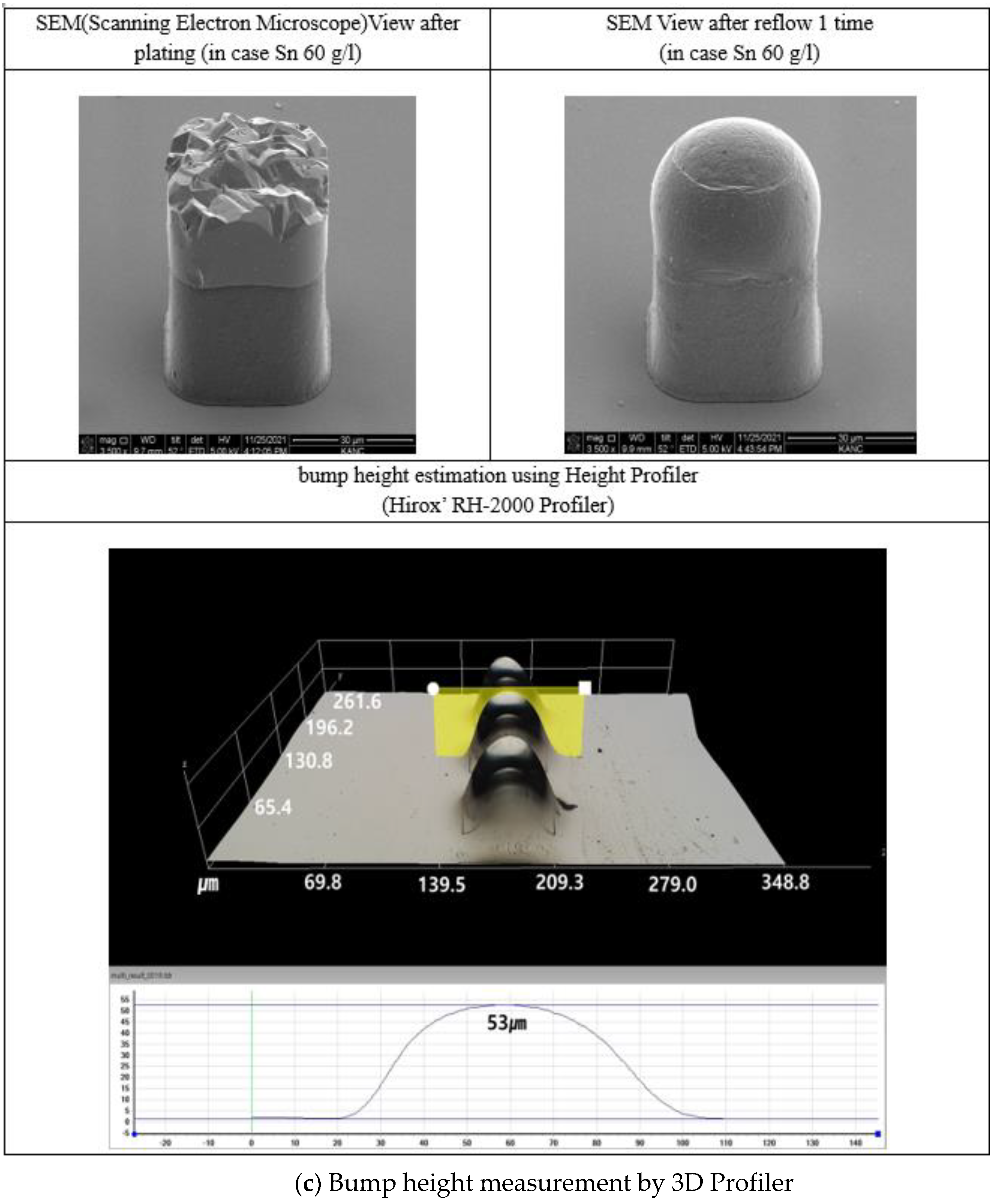
Figure 1 shows the Sn plating system manufactured to evaluate the shape and height of the Sn bump. Figure 1a shows the characteristics and configuration diagram of the plating equipment. This plating equipment is divided into a cleaning chamber and an electroplating chamber as a whole. The plating process is as follows: First, the wafer injected into the first chamber was cleaned. In the next stage of the chamber, an anode was observed, and Cu electroplating was performed. Cleaning was carried out again, and Sn was electroplated. Finally, when the cleaning was finished and the dry films were lifted off, the microbump pattern on the wafer was completed. Figure 1b shows the design of the bump to be formed by plating on the wafer. The bump was 30 µm in diameter and 55 µm in spacing. Ti seed was deposited on the wafer. The dry film 50 µm in thickness was then applied and opened. After that, Cu/Ni/Cu was plated in order. Pure Sn plating was then performed. Finally, the dry film and Ti were removed. After selecting 16 randomly plated bumps in a die of a 4-inch wafer, measurement points were measured and evaluated. The height of the bump was measured based on the center of the bump formed by plating. Figure 1c shows the method for evaluating the height of the bump. For example, the bump shape was examined before and after reflow formed in the Sn 60 g/L condition. The formed bump was photographed. Its height was evaluated with a HIROX’ RH-2000 Profiler. Based on previous experiments, the acid and leveler, plating bath capacity, flow rate, and plating time of the plating system were fixed at 165 g/L, 1 mL/L, 120 mL/L, 7 L, 3.5 L/min, and 3 min, respectively. As the main key process parameter of the plating system, the height of the bump was evaluated while changing the Sn concentration, temperature, current density, and additive concentration.
(b)
Observation of Changes in Pure Sn Concentration
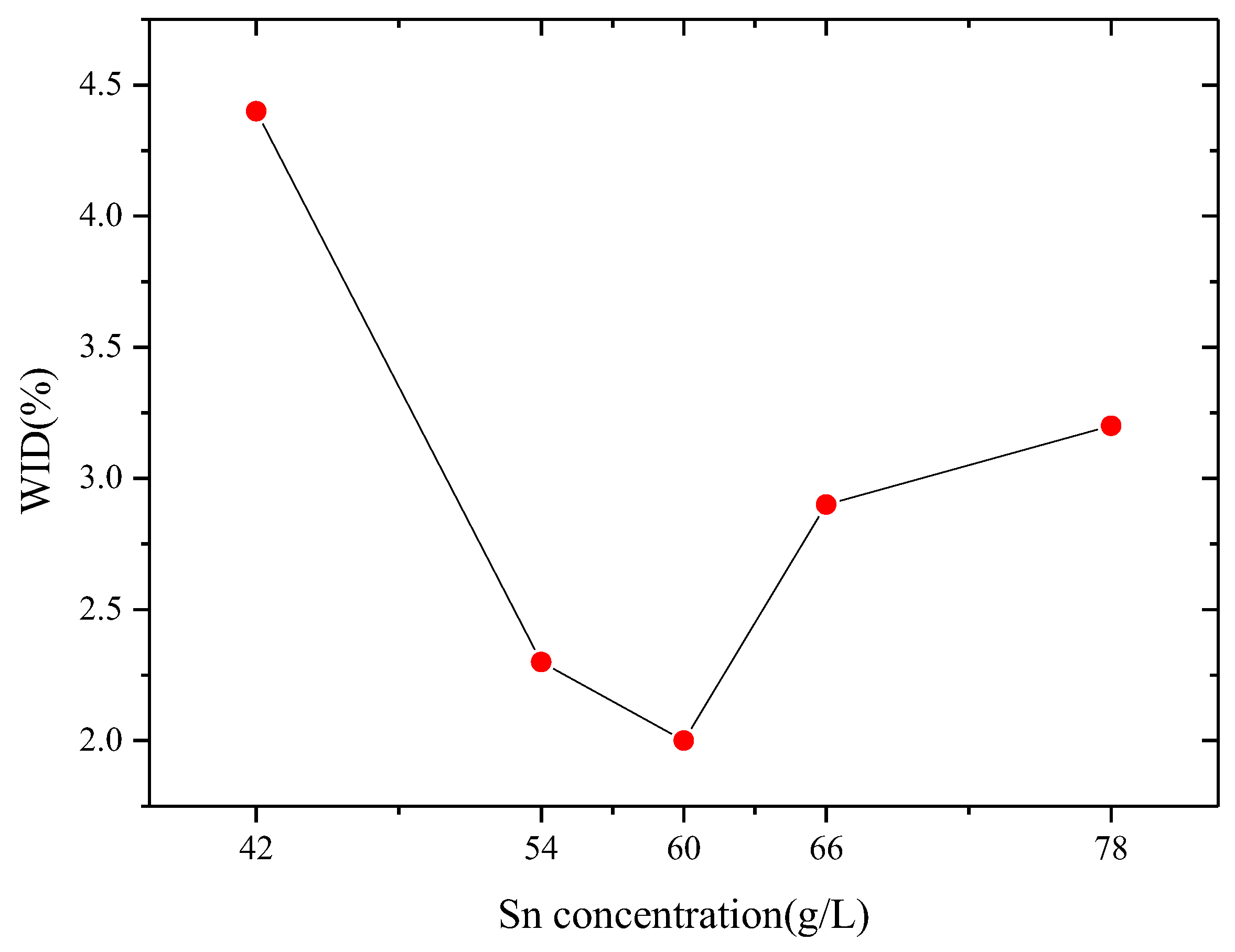
Table 1 shows evaluation values of the bump height, average max-min, and WID (%) according to the pure Sn concentration. Pure Sn concentrations were in the order of 42, 54, 60, 66, and 78 g/L. These findings confirmed the overall shape, surface condition at the top, and roundness of bumps formed depending on the concentration of the Sn plating solution. At this time, at least 16 bump samples (P1–P16) on the wafer were randomly selected and evaluated. As the Sn concentration increased, deviations in the sizes of the center and the outside increased, and the roundness tended to improve. When the Sn concentration was 60 g/L, the average value of the height was 55.0 µm, with maxim-minim of 2.2 µm. (Table 2) In addition, as shown in Figure 2, the result of measuring the sample by location according to the concentration confirmed the lowest deviation in height uniformity (WID) of approximately 2% with an average of 55.0 µm and a max-min of 2.2 µm when the Sn concentration was 60 g/L (Figure 2).
(c)
Observation of Sn bump Changes in Additive
The shape of the bump was observed after adding additives to determine whether the additive concentration could affect the Sn bump. At this time, the additive concentration was 120 mL/L. After adding additives, changes in the Sn concentration were made to observe the shape of the bump, surface conditions at the top, and roundness. When the Sn concentration in the additive was 60 g/L, the average value of height was 55.0 µm and the maximum-minimum was 2.2 um (Table 3). It was confirmed that the height uniformity (WID) was the lowest at ± 2.0% when Sn at 60 g/L was added (Figure 3).
(d)
Observation of changes in plating process temperature
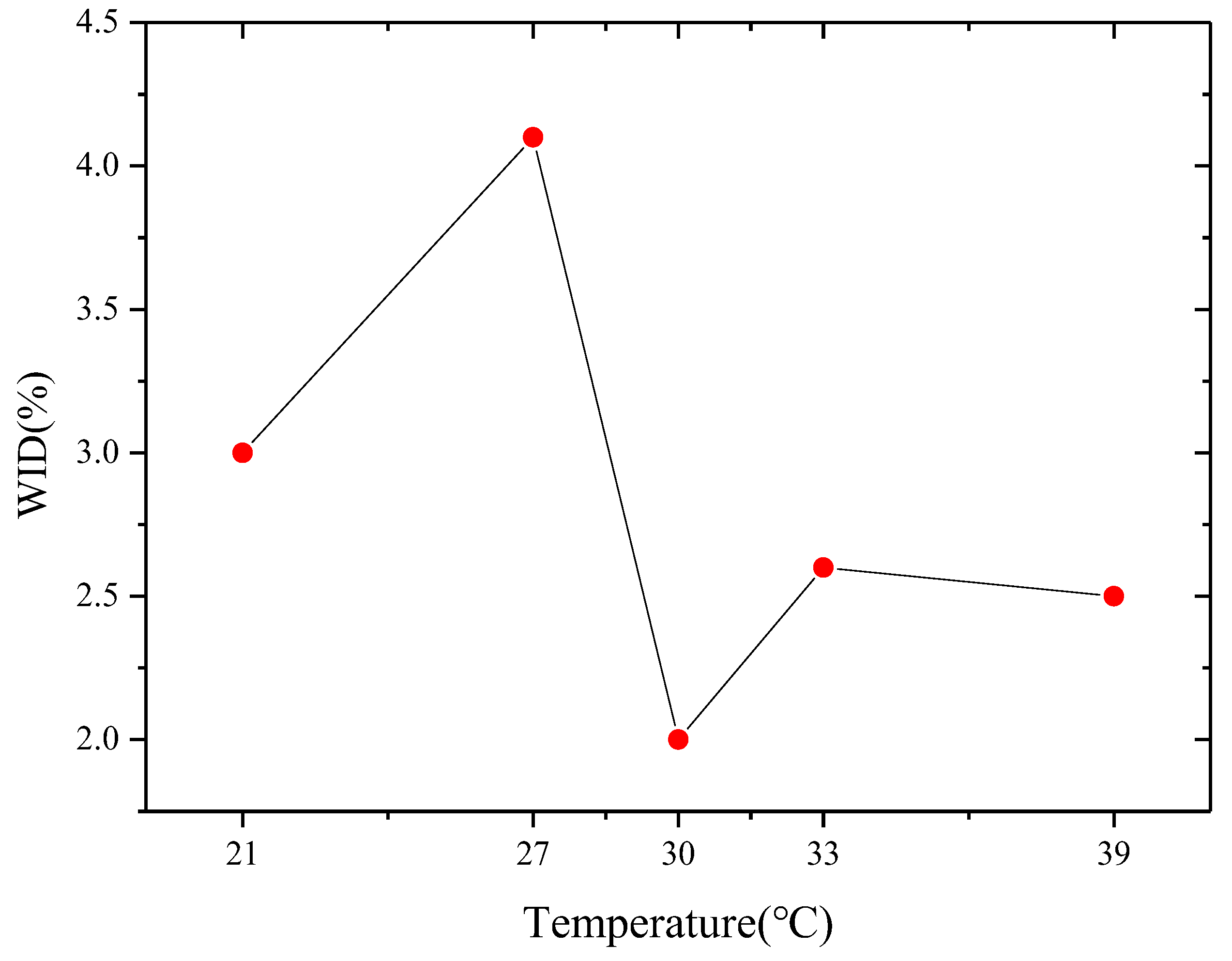
The plating process temperature was carried out in the order 21, 27, 30, 33, and 39 °C. The shape of the bump formed by the temperature, the surface state of the top, and the roundness was observed. As shown in Figure 4, analysis results showed that as the process temperature increased, deviations of sizes at the center and outside decreased and the roundness tended to improve. When the plating process temperature was 30 °C, the average value of height was 55.0 µm and the maximum-minimum was 2.2 um (Table 4). As shown in Figure 4, when observed by the sample measurement location, the shape of the bump had the lowest deviation of WID ± 2% at 30 °C.
(e)
Observation of changes in current density (ASD: Ampere per Square Decimeter)
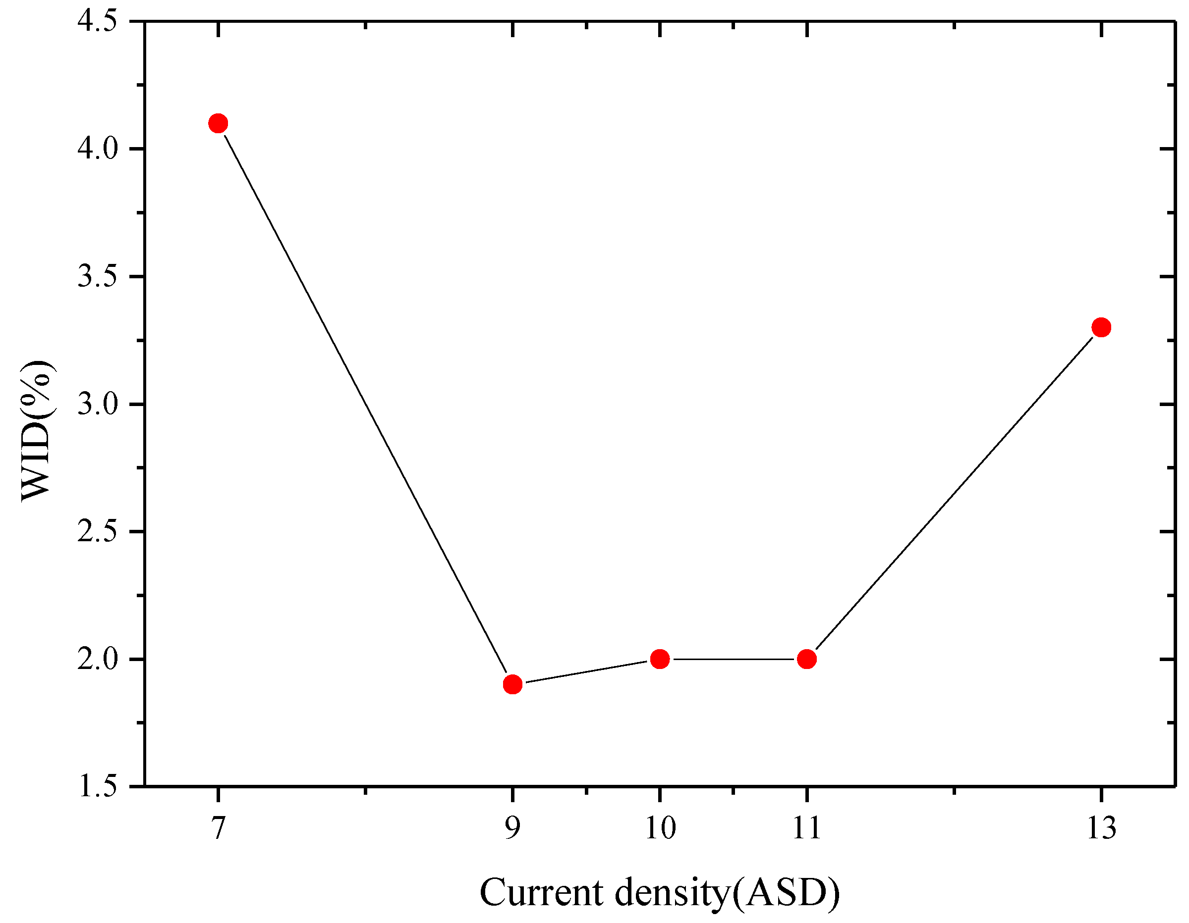
To observe changes in the height deviation caused by the current density of the Sn bump, different current densities (7, 9, 10, 11, and 13 ASD) were used. When the current density was 9 ASD, the average value of the height was 55.5 µm and the maximum and minimum was 2.1 um (Table 5). The lowest deviation of WID was 1.9% at a current density of 9 ASD (Figure 5). Therefore, in forming the bump, the conditions of a temperature of 30 °C and a current of 9 ASD were the most optimal conditions, and the bump deviation was also small.
(f)
Verifying the formation of a void
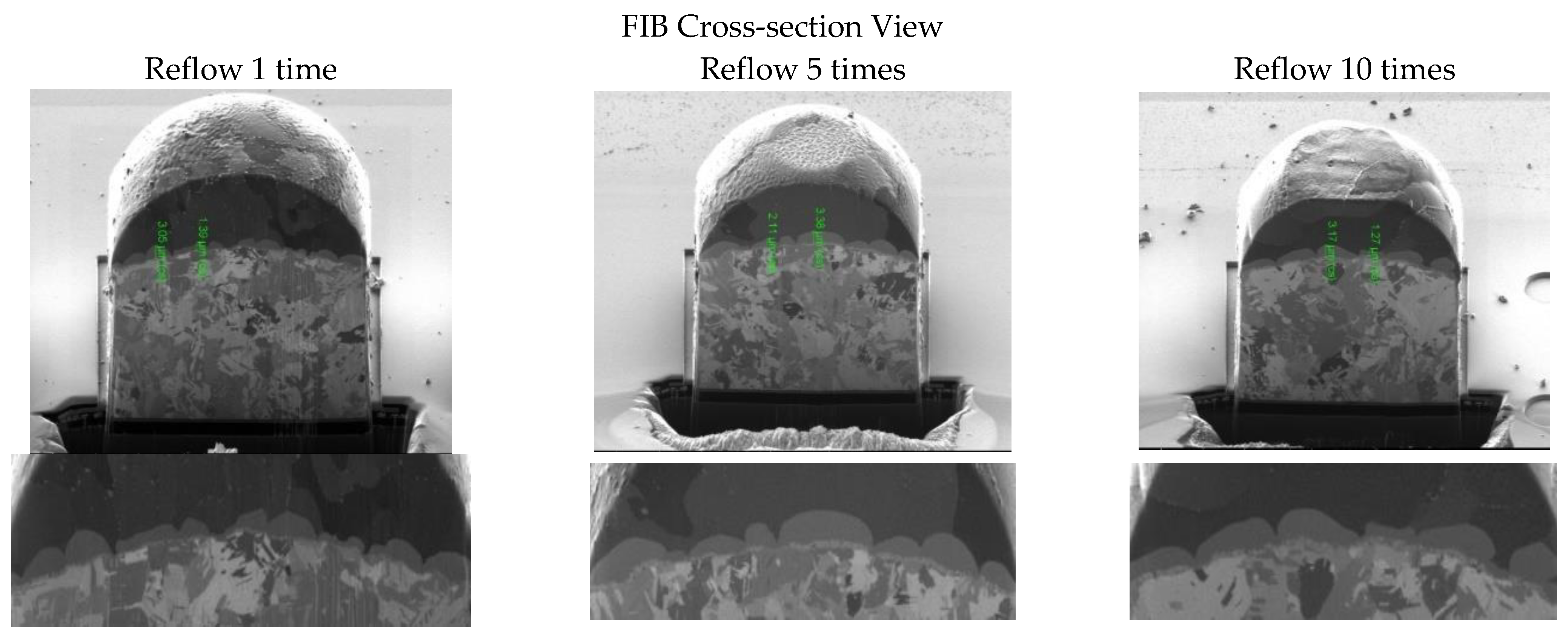
The Sn bump was manufactured using the plating material and process conditions described so far, and the manufactured bump was verified by cutting its cross-section. When metals of different types are bonded to each other, a Kirkendall effect occurs, in which atoms of metals with a high diffusion speed will move a lot toward the slow metal and the interface moves toward the fast side, forming a Kirkendall void on the metal with a high diffusion speed [18,19]. As the number of reflows increases, this void will form more and more [20,21]. As the size and number of voids increase, the bonding strength and reliability will decrease. Therefore, after the bump was produced, a cross-sectional void was observed through a focus ion beam (FIB). Figure 6 shows an SEM image of the cross-section observed after 1, 5, and 10 iterations of reflow. As shown in Figure 6, the void was not evident in the plated Sn plating bump. Voids at the IMC and Sn interfaces or the IMC and Cu interfaces were not observed.
Table 6 below summarizes the actual loss results determined for the eight plating materials and process conditions described so far. In addition, the shape of a pure Sn bump with a diameter of 30 µm was observed before and after the reflow.
2.
Preparation of samples for evaluating the shear strength of the pure Sn
(a)
Observation of Sn plating thickness uniformity on 4-inch wafer
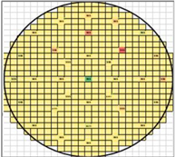
Using the process conditions and facilities presented in Table 1, Sn plating was performed instead of a bump using electroplating on a 4-inch wafer. First of all, the purpose of Sn plating on a 4-inch wafer was to ensure uniformity of the plating thickness according to the distance between electrodes, shielding distance, and current density. The plating thickness deviation was then evaluated. The evaluation sample was deposited with Ti 1000 Å on the wafer as a seed material. During electroplating, the distance between electrodes was classified as 155 mm and 115 mm. The cathode electrode and the shielding distance were classified as 65 mm at the inter-pole distances of 115 mm and 155 mm, respectively. The shielding distance was classified as 65 mm and 35 mm. At a current density of 9 ASD, a temperature of 30 °C, and a velocity of flow of 3.5 L/min, the Sn thickness was plated to 20 μm. Ten plated Sn bumps were randomly selected to measure the plating thickness. As summarized in Table 7, the WIW thickness uniformity showed a deviation of ± 3.88% under the following conditions: An anode–cathode distance of 115 mm, a shielding distance of 65 mm, and a shielding size of 65 mm. Figure 7 is the final image of the pure Sn micro bump designed above.
(b)
Results of pure Sn bump geometry formed by plating
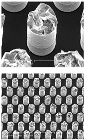
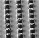
A 30 µm pure Sn bump was formed with plating equipment as shown in Figure 2a. Optimal plating conditions are shown in Table 2. Figure 8a shows a reflow profile of the pure Sn bump. Before reflowing, the Sn bump was formed by plating, and flux was applied to the bump followed by reflowing. The step-by-step process of the reflow proceeded in a total of five stages: The ramp-to-sock section, pre-heating section, ramp-to-peak section, reflow section, and cooling section [20,21,22]. Figure 8a shows the temperature range of each stage over time. Figure 8b shows the Sn bump fabricated with a bump diameter of 30 µm and a spacing of 55 µm. This figure shows the shape of the bump before and after reflow using SEM. The sample was prepared according to the number of reflows to evaluate the shear strength. Reflow was conducted 1, 3, 5, 7, and 10 times for five samples.
Table 8 shows the evaluation method, measurement location, and shape before and after the reflow for pure Sn bumps manufactured on 4-inch wafers. WID and WIW were evaluated at three locations on the wafer (#1, #2, and #3). The measurement was performed only for the height at which the pure Sn was plated. The height was then evaluated for WID and WIW. From Table 9, the mean height was 24.02 µm and the Max-Min height was 0.4 µm, which gave a WID of 1.7% for #2 (Table 10). Table 10 shows the WIW evaluation results for #1, #2, and #3. The mean was 24.02 µm and the Max-Min was 0.9 µm, resulting in a deviation of WIW of ± 1.9% for #2.

3. Results and Discussion

(a)
Shear test and evaluation
After the reflow, a shear test was performed to confirm the shear strength of the joint between Cu and Sn [23]. The shear test used DAGE4000+ equipment. DAGE 4000+ shows more reliable results when testing micro bumps with an acuity of 0.1% or less compared to conventional shear test equipment. It is also possible to install a fine tool and jaw to perform a micro bump test. The size of the jaw used in this experiment was 50 µm. The height of the shear was placed at 22 µm from the bottom of the manufactured bump. It then proceeded at a speed of 100 µm/s [24]. After performing a number of shear tests, the shear strength for each reflow was quantified. To analyze the correlation between the metal growth and shear strength of the solder junction of the bump, the cross-sectional area of the intermetallic compound was schematized using plasma-FIB (Focused Ion Beam). Three bump samples were prepared for different numbers (1, 3, 5, 7, and 10) of reflows. These prepared samples were sheared according to the measurement method and conditions of DAGE 4000+. Figure 9 is a SEM image showing the boundary between the Cu and Sn bump with a shear height of 22 µm.
For the value shown in Table 11, as illustrated in Figure 10 below, the shear strength between Cu and Sn was measured with 1, 3, 5, 7, and 10 reflows [25].
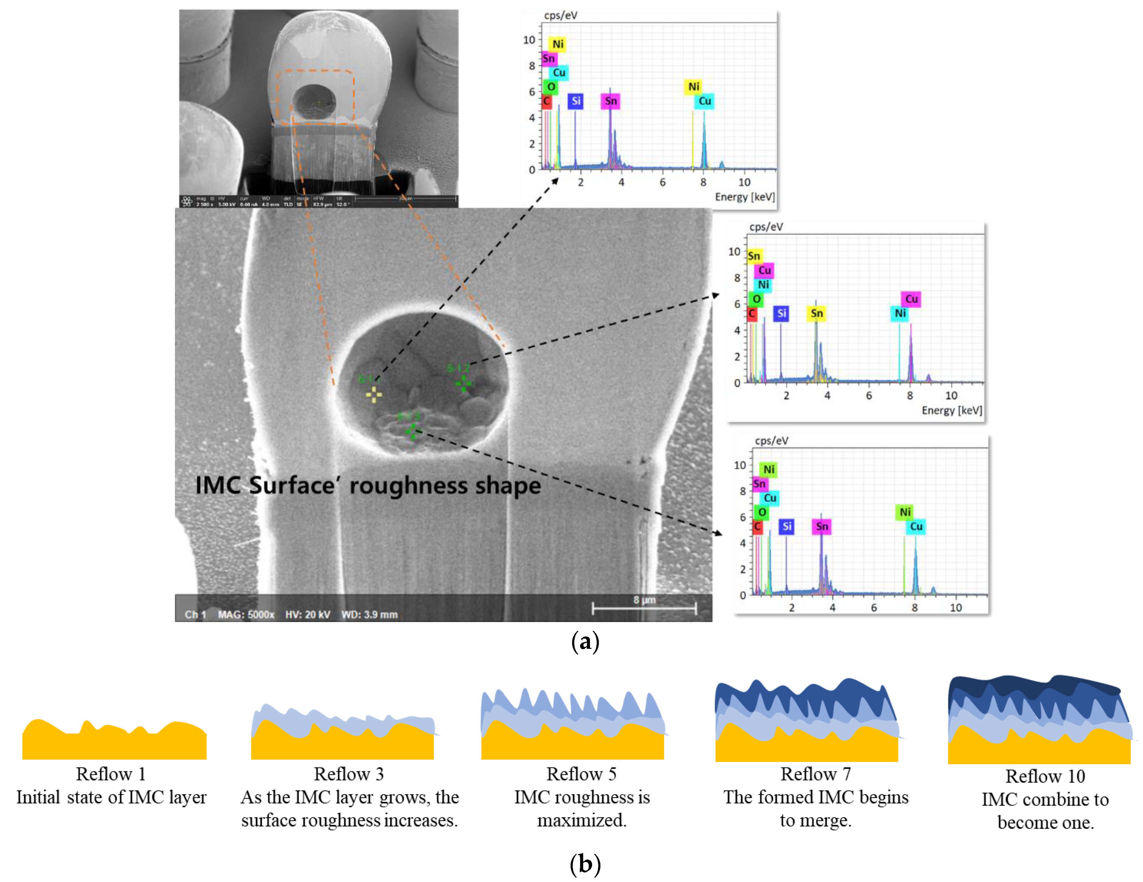
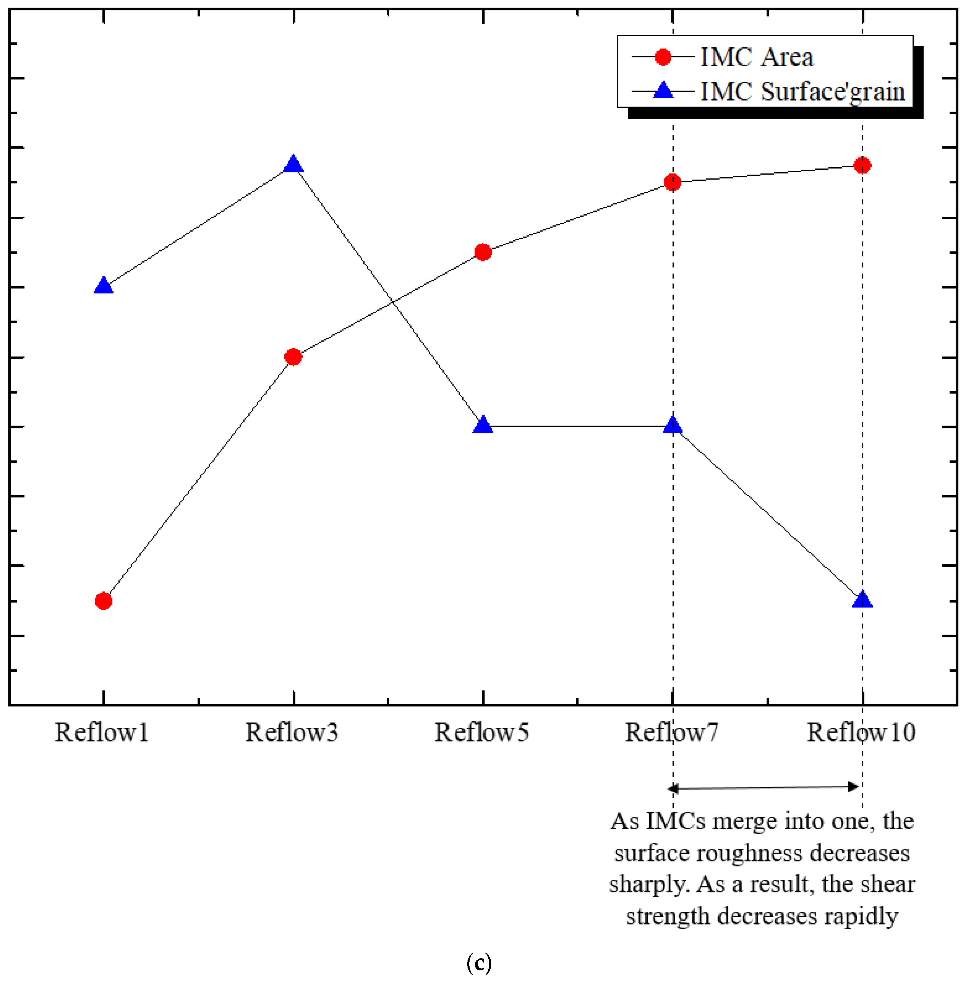
The shear strength for one reflow was 5.314 gf. As shown in the graph above, it was observed that the shear strength rapidly increased up to three reflows. From 3 to 7 times, the value of the shear strength remained the same without a significant change. In the last 10 reflows, it was confirmed that the intensity dropped rapidly. The reason is explained in Figure 11. Figure 11a shows the cause in the shape of the Sn bump cross-section. SEM images verified that the cross-sectional shape of the Sn bump and the internal roughness between the IMC layer were formed inside a round cross-section. The surface roughness of the IMC might vary significantly in size and shape depending on the number of reflows. Figure 11b is a schematic of the process formed for the surface shape of IMC according to the number of reflows. Changes in the surface state of the IMC according to the number of reflows can immediately affect the shear strength of the bump. Figure 11c shows the correlation between the surface roughness and cross-sectional area based on the IMC cross-sectional area and the shear strength value of the manufactured bump. As shown in Figure 11c, as the number of reflows increases, the number of grains decreases, and the shape of the valley between grains increases proportionally.
(b)
Growth of IMC (Inter-Metallic Compound)
To determine the cause of the change in shear strength according to the number of reflows after the shear test of the Cu/Sn micro bump, the growth of the IMC of the junction was analyzed. The cross-section of the Sn bump was analyzed using plasma–FIB. The area and shape of the cross-section of the IMC were noted [26,27,28,29,30,31]. The analysis confirmed that the cross-sectional area of the IMC of the Sn bump increased rapidly. The area of growth of the IMC slowed after a certain number of reflows (Figure 12). Initially, when an adhesive surface between Cu and Sn was observed, a flat state without bending was maintained. As a result, the shear strength was low. In the case of three to five reflows or three to seven reflows, the adhesive surface of Cu and Sn changed more actively in the IMC, which was an alloy state of Cu and Sn, resulting in more curvature than in the initial stage. In addition, as the number of reflow cycles increased, the IMC thickness increased, resulting in a sharp drop in shear strength value regardless of the IMC surface roughness. To prove that this phenomenon occurs, the surface state of the Cu/Sn alloy after the cross-section of the bump in Figure 13 confirms that the roughness changed according to the number of reflows. If the roughness of IMC is quantified after removing only the Sn bump, the behavior mechanism according to the cause is expected to be found.

4. Conclusions

In this study, we formed a pure Sn bump with a diameter of 30 µm with height uniformity using an electroplating method for the solder cap on the Cu post/Ni barrier. With the development of the packaging industry and the miniaturization of the bump becoming increasingly important, microbumps need to be smaller in size through electroplating. Conditions applied in this experiment included Sn, acid, and additive concentrations, temperature, plating bath capacity, current density, plating time, and flow rate. Their optimal experimental values measured were 60 g/L, 165 g/L, 120 mL/L, 30 °C, 7 L, 9 ASD, 3 min, and 35 L/min, respectively. Pure Sn microbumps with a diameter of 30 µm were uniformly plated based on the estimation of WIW/WID. As the number of reflows increased, IMCs in the island format gradually merged into one mass, reducing the roughness and sharply decreasing the shear strength. In the case of finer Sn bumps, shear strength measurements are very important. From this experiment, it was judged that the thickness of the IMC and the shape and size of the grain affected the shear strength. In the future, we plan to three-dimensionally analyze the thickness of IMC and the shape of the grain for both plane sections and cross-sections. If 20 µm pure Sn plated up to the IMC layer is removed, clear results will be obtained regarding the number, shape, and thickness of grains. For the future, we are working on a pure Sn bump with a diameter of 20 µm and a height of 30 um. It is difficult to precisely analyze how the number of IMC grains grows during reflow, but it is an important aspect to study. Therefore, it seems necessary to study whether the shear strength values of micro bumps are applicable to 3D micro interconnection.

Author Contributions

In this paper, the first author, C.-Y.N., contributed to the experimental design, perform all experiment and study correlation between IMC and shear test. B.-M.J. contributed to the supporting experiment and design. J.-W.K., W.-S.J. and J.-S.J. contributed to the selecting material and equipment maintenance. And lastly, corresponding author, S.-M.C. and H.-S.P., contributed to experimental summary, process design. The preparation of the original draft manuscript and writing were carried out by C.-Y.N. Also, review and editing were carried out C.-Y.N., S.-M.C. and H.-S.P. All authors have read and agreed to the published version of the manuscript.

Funding

This research was funded by Advanced Technology Center (ATC) grant number 20009262, and Next Generation Intelligence Semiconductor Foundation grant number 20011257.

Data Availability Statement

All data that is backed up can be found in this paper.

Acknowledgments

This work was supported by the Advanced Technology Center (20009262, A Development of Advanced Bumping Technology for Super Integrated Circuit in 12 inch Wafer Level Packaging). This work was also supported by the Next Generation Intelligence Semiconductor Foundation (20011257, HBM, large-area wafer (12″), fine pattern wafer, next-generation semiconductor, micro bump technology, High-purity refining).

Conflicts of Interest

The authors declare no conflict of interest.

References

  1. De Vos, J.; Jourdain, A.; Erismis, M.; Zhang, W.; De Munck, K.; La Manna, A.; Tezcan, D.S.; Soussan, P. High density 20 μm pitch CuSn microbump process for high-end 3D applications. In Proceedings of the 2011 IEEE 61st Electronic Components and Technology Conference (ECTC), Lake Buena Vista, FL, USA, 31 May–3 June 2011; pp. 27–31. [Google Scholar]
  2. Son, H.; Noh, S.; Jung, H.; Lee, W.; Oh, J.; Kim, N. Reliability studies on micro-bumps for 3-D TSV integration. In Proceedings of the 2013 IEEE 63rd Electronic Components and Technology Conference, Las Vegas, NV, USA, 28–31 May 2013; pp. 29–34. [Google Scholar]
  3. Ohara, Y.; Noriki, A.; Sakuma, K.; Lee, K.W.; Murugesan, M.; Bea, J.; Yamada, F.; Fukushima, T.; Tanaka, T.; Koyanagi, M. 10 µm fine pitch Cu/Sn micro-bumps for 3-D super-chip stack. In Proceedings of the 2009 IEEE International Conference on 3D System Integration, San Francisco, CA, USA, 28–30 September2009; pp. 1–6. [Google Scholar]
  4. Xiong, W.; Qi, L.; Luo, J.; Zhang, D.; Liang, J.; Yi, H. Experimental investigation on the height deviation of bumps printed by solder jet technology. J. Mater. Process. Technol. 2017, 243, 291–298. [Google Scholar] [CrossRef]
  5. Lee, J.-B. Semiconductor Memory Road Map: Advances in Semiconductor Memory. IEEE Solid-State Circuits Mag. 2016, 8, 66–74. [Google Scholar] [CrossRef]
  6. Kim, K. Silicon technologies and solutions for the data-driven world. In Proceedings of the 2015 IEEE International Solid-State Circuits Conference, San Francisco, CA, USA, 22–26 February2015; pp. 1.1.1–1.1.9. [Google Scholar]
  7. Kang, U. 8 Gb 3-D DDR3 DRAM using through-silicon-via technology. IEEE J. Solid-State Circuits 2010, 45, 115–119. [Google Scholar] [CrossRef]
  8. Smith, K.; Hanaway, P.; Jolley, M.; Gleason, R.; Strid, E.; Daenen, T.; Dupas, L.; Knuts, B.; Marinissen, E.J.; Van Dievel, M. Evaluation of TSV and micro-bump probing for wide I/O testing. In Proceedings of the 2011 IEEE International Test Conference, Anaheim, CA, USA, 20–22 September 2011; pp. 1–10. [Google Scholar]
  9. Yoon, S.W.; Ku, J.H.; Suthiwongsunthorn, N.; Marimuthu, P.C.; Carson, F. Fabrication and packaging of microbump interconnections for 3D TSV. In Proceedings of the 2009 IEEE International Conference on 3D System Integration, San Francisco, CA, USA, 28–30 September 2009; pp. 1–5. [Google Scholar]
  10. Lee, J.; Lee, C.Y.; Kim, C.; Kalchuri, S. Micro Bump System for 2nd Generation Silicon Interposer with GPU and High Bandwidth Memory (HBM) Concurrent Integration. In Proceedings of the 2018 IEEE 68th Electronic Components and Technology Conference (ECTC), San Diego, CA, USA, 29 May–1 June 2018; pp. 607–612. [Google Scholar]
  11. Arai, S.; Akatsuka, H.; Kaneko, N. Sn-Ag Solder Bump Formation for Flip-Chip Bonding by Electroplating. J. Electrochem. Soc. 2003, 150, C730. [Google Scholar] [CrossRef]
  12. Sahaym, U.; Miller, S.L.; Norton, M.G. Effect of plating temperature on Sn surface morphology. Mater. Lett. 2010, 64, 1547–1550. [Google Scholar] [CrossRef]
  13. Wright, S.L.; Tsang, C.K.; Maria, J.; Dang, B.; Polastre, R.; Andry, P.; Knickerbocker, J. Micro-interconnection reliability: Thermal, electrical and mechanical stress. In Proceedings of the 2012 IEEE 62nd Electronic Components and Technology Conference, San Diego, CA, USA, 29 May–1 June 2012; pp. 1278–1286. [Google Scholar]
  14. Hsiao, H.-Y.; Trigg, A.D.; Chai, T.C. Failure Mechanism for Fine Pitch Microbump in Cu/Sn/Cu System During Current Stressing. IEEE Trans. Compon. Packag. Manuf. Technol. 2015, 5, 314–319. [Google Scholar] [CrossRef]
  15. Jung, H.-R.; Kim, H.-H.; Lee, W.-J. Characterization of small-sized eutectic Sn-Bi solder bumps fabricated using electroplating. J. Electron. Mater. 2006, 35, 1067–1073. [Google Scholar] [CrossRef]
  16. Tanida, K.; Umemoto, M.; Tanaka, N.; Tomita, Y.; Takahashi, K. Micro Cu Bump Interconnection on 3D Chip Stacking Technology. Jpn. J. Appl. Phys. 2004, 43, 2264–2270. [Google Scholar] [CrossRef]
  17. Na, S.-H.; Lim, S.-K.; Kim, J.-S.; Park, H.-S.; Oh, H.-J.; Choi, J.-W.; Suh, S.-J. Experimental study of bump void formation according to process conditions. Microelectron. Reliab. 2013, 53, 638–644. [Google Scholar] [CrossRef]
  18. Mei, Z.; Ahmad, M.; Hu, M.; Ramakrishna, G. Kirkendall voids at Cu/solder interface and their effects on solder joint reliability. In Proceedings of the Electronic Components and Technology, 2005, ECTC ’05, Lake Buena Vista, FL, USA, 1 May–3 June 2005; Volume 1, pp. 415–420. [Google Scholar]
  19. Zhou, S.; Zhang, Y.-B.; Gao, L.-Y.; Li, Z.; Liu, Z.-Q. The self-healing of Kirkendall voids on the interface between Sn and (1 1 1) oriented nanotwinned Cu under thermal aging. Appl. Surf. Sci. 2022, 588, 152900. [Google Scholar] [CrossRef]
  20. Liang, Y.C.; Chen, C.; Tu, K.N. Side Wall Wetting Induced Void Formation due to Small Solder Volume in Micro bumps of Ni/SnAg/Ni upon Reflow. ECS Solid State Lett. 2012, 1, P60. [Google Scholar] [CrossRef]
  21. Liu, H.; Xu, C.; Liu, X.; Yu, D.; Dai, F.; Lu, Y.; Shangguan, D. Effect of IMC growth on thermal cycling reliability of micro solder bumps. In Proceedings of the 2013 IEEE 15th Electronics Packaging Technology Conference (EPTC 2013), Singapore, 11–13 December 2013; pp. 836–839. [Google Scholar]
  22. Li, M.-L.; Zhang, L.; Jiang, N.; Zhong, S.-J.; Zhang, L. Influences of silicon carbide nanowires’ addition on IMC growth behavior of pure Sn solder during solid–liquid diffusion. J. Mater. Sci. Mater. Electron. 2021, 32, 18067–18075. [Google Scholar] [CrossRef]
  23. Lee, Y.-H.; Lee, H.-T. Shear strength and interfacial microstructure of Sn–Ag–xNi/Cu single shear lap solder joints. Mater. Sci. Eng. A 2007, 444, 75–83. [Google Scholar] [CrossRef]
  24. Pang, J.H.; Low, T.H.; Xiong, B.S.; Luhua, X.; Neo, C.C. Thermal cycling aging effects on Sn–Ag–Cu solder joint microstructure, IMC and strength. Thin Solid Films 2004, 462–463, 370–375. [Google Scholar] [CrossRef]
  25. Chan, Y.; So, A.C.; Lai, J. Growth kinetic studies of Cu–Sn intermetallic compound and its effect on shear strength of LCCC SMT solder joints. Mater. Sci. Eng. B 1998, 55, 5–13. [Google Scholar] [CrossRef]
  26. Xu, L.; Pang, J.H. Nano-indentation characterization of Ni–Cu–Sn IMC layer subject to isothermal aging. Thin Solid Films 2006, 504, 362–366. [Google Scholar] [CrossRef]
  27. Hou, L.; Moelans, N.; Derakhshandeh, J.; De Wolf, I.; Beyne, E. Study of the effect of Sn grain boundaries on IMC morphology in solid state inter-diffusion soldering. Sci. Rep. 2019, 9, 14862. [Google Scholar] [CrossRef] [Green Version]
  28. Kunwar, A.; Coutinho, Y.A.; Hektor, J.; Ma, H.; Moelans, N. Integration of machine learning with phase field method to model the electromigration induced Cu6Sn5 IMC growth at anode side Cu/Sn interface. J. Mater. Sci. Technol. 2020, 59, 203–219. [Google Scholar] [CrossRef]
  29. Guo, B.; Ma, H.; Kunwar, A.; Chu, X. Effect of the degree of super cooling on growth mechanism of Cu6Sn5 in pure Sn/Cu solder joint. J. Mater. Sci. Mater. Electron. 2021, 32, 7528–7540. [Google Scholar]
  30. Datta, M. Manufacturing processes for fabrication of flip-chip micro-bumps used in microelectronic packaging: An overview. J. Micromanuf. 2019, 3, 69–83. [Google Scholar] [CrossRef]
  31. Ma, X.; Qian, Y.; Yoshida, F. Effect of La on the Cu–Sn intermetallic compound (IMC) growth and solder joint reliability. J. Alloys Compd. 2002, 334, 224–227. [Google Scholar] [CrossRef]
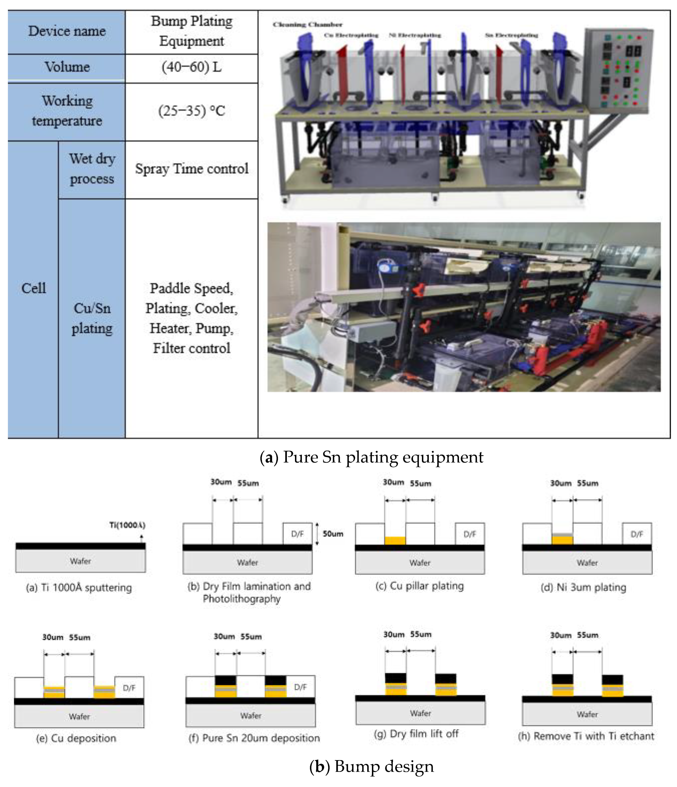
Figure 1. (a) Sn Plating System, (b) Design, and (c) Bump height measurement for Sn Bump Formation.
Electronics 12 00144 g001aElectronics 12 00144 g001b
Figure 2. Height deviation of bump according to Sn concentration, WID.
Electronics 12 00144 g002
Figure 3. Height deviation of bump when additive is added, WID.
Electronics 12 00144 g003
Figure 4. Height deviation of bump according to temperature variation, WID.
Electronics 12 00144 g004
Figure 5. Height deviation of bump by current density, WID.
Electronics 12 00144 g005
Figure 6. Cross-section images of Sn bump with one reflow.
Electronics 12 00144 g006
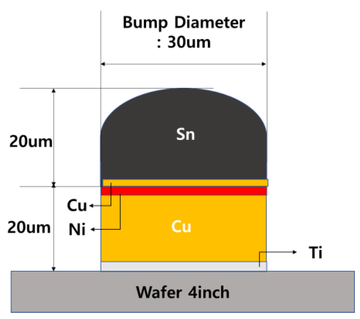
Figure 7. Pure Sn bump formation design with a diameter of 30 µm.
Electronics 12 00144 g007
Figure 8. Pure Sn bumps manufactured on 4-inch wafers. (a) Reflow profile, (b) Pure Sn bump before reflow, and (c) Pure Sn bump after reflow.
Electronics 12 00144 g008aElectronics 12 00144 g008b
Figure 9. SEM image after shear test.
Electronics 12 00144 g009
Figure 10. Maximum, minimum, and average values of shear strength according to the number of reflows.
Electronics 12 00144 g010
Figure 11. Correlation between IMC Formation Mechanism and Shear Strength. (a) IMC inner Section Shape, (b) IMC formation process, (c) Correlation between roughness and area.
Electronics 12 00144 g011aElectronics 12 00144 g011b
Figure 12. IMC area cross-section graph by the number of reflows.
Electronics 12 00144 g012
Figure 13. Cross-sectional shape and area of the micro bump.
Electronics 12 00144 g013
Table 1. Evaluation method for each process of the pure Sn bump.
Experimental ConditionEvaluation Method
Current Density/Time(7–13) ASD/3 min
MaterialsSn Concentration(40–80) g/LHeight Uniformity (WID)
= (Max–Min)/Avg × 100
Observation of the surface of the plated bump
ACID Concentration165 g/L
Additive concentration120 mL/L
Process conditionTemperature(20–40) °C
Plating cell capacity7 L
Velocity of flow3.5 L/min
Table 2. Condition and measurement of Sn concentration.
ConditionBump Height (µm)Average
(µm)
Max-Min
(µm)
WID
(%)
Sn 42 g/LP1P2P3P4P5P6P7P854.64.8±4.4
54.856.053.753.852.353.355.952.7
P9P10P11P12P13P14P15P16
54.053.756.053.452.756.557.157.0
Sn 54 g/LP1P2P3P4P5P6P7P857.12.6±2.3
56.355.857.556.956.756.756.558.3
P9P10P11P12P13P14P15P16
58.457.457.256.857.956.557.157.0
Sn 60 g/LP1P2P3P4P5P6P7P855.02.2±2.0
54.954.954.756.055.554.755.156.0
P9P10P11P12P13P14P15P16
55.055.454.655.554.953.854.554.1
Sn 66 g/LP1P2P3P4P5P6P7P854.33.2±2.9
53.954.454.053.754.753.955.555.9
P9P10P11P12P13P14P15P16
55.952.752.954.454.454.653.853.8
Sn 78 g/LP1P2P3P4P5P6P7P856.63.6±3.2
57.456.457.855.555.157.658.355.5
P9P10P11P12P13P14P15P16
55.157.457.856.254.755.657.656.8
Table 3. Condition and measurement of additive.
ConditionBump Height (µm)Average
(µm)
Max-Min (µm)WID
(%)
Additive
Add.
42 mL/L
P1P2P3P4P5P6P7P852.54.1±3.9
52.552.953.050.253.553.552.652.3
P9P10P11P12P13P14P15P16
52.351.953.052.752.051.952.154.3
Additive
Add.
54 mL/L
P1P2P3P4P5P6P7P854.94.0±3.6
55.956.752.756.154.854.656.355.3
P9P10P11P12P13P14P15P16
54.654.953.256.155.754.154.054.0
Additive
Add.
60 mL/L
P1P2P3P4P5P6P7P855.02.2±2.0
54.954.954.756.055.554.755.156.0
P9P10P11P12P13P14P15P16
55.055.454.655.554.953.854.554.1
Additive
Add.
66 mL/L
P1P2P3P4P5P6P7P854.64.1±3.8
54.854.452.555.254.355.453.955.1
P9P10P11P12P13P14P15P16
55.153.853.956.655.154.754.853.9
Additive
Add.
78 mL/L
P1P2P3P4P5P6P7P854.76.8±6.2
54.054.652.755.854.854.254.557.7
P9P10P11P12P13P14P15P16
57.853.251.056.256.153.454.354.4
Table 4. Condition and measurement of Sn microbumps by temperature change.
ConditionBump Height (µm)Average
(µm)
Max-Min (µm)WID
(%)
21 °CP1P2P3P4P5P6P7P854.93.3±3.0
55.556.055.255.255.354.655.755.3
P9P10P11P12P13P14P15P16
55.154.954.154.354.952.755.154.1
27 °CP1P2P3P4P5P6P7P853.74.5±4.2
52.853.553.254.353.453.154.454.7
P9P10P11P12P13P14P15P16
56.553.152.752.052.552.654.954.7
30 °CP1P2P3P4P5P6P7P855.02.2±2.0
54.954.954.756.055.554.755.156.0
P9P10P11P12P13P14P15P16
55.055.454.655.554.953.854.554.1
33 °CP1P2P3P4P5P6P7P854.02.8±2.6
53.053.253.654.755.654.354.855.7
P9P10P11P12P13P14P15P16
55.553.353.153.954.353.353.452.9
39 °CP1P2P3P4P5P6P7P856.62.8±2.5
57.757.956.057.157.056.555.258.0
P9P10P11P12P13P14P15P16
58.055.556.256.956.255.755.955.5
Table 5. Condition and measurement of Sn microbumps by current density.
ConditionBump Height (µm)Average
(µm)
Max-Min (µm)WID
(%)
7ASDP1P2P3P4P5P6P7P854.84.5±4.1
54.454.754.557.856.753.855.655.4
P9P10P11P12P13P14P15P16
54.354.953.855.155.453.653.753.3
9ASDP1P2P3P4P5P6P7P855.52.1±1.9
55.055.456.456.056.356.356.056.2
P9P10P11P12P13P14P15P16
56.255.855.354.455.154.354.654.8
10ASDP1P2P3P4P5P6P7P855.02.2±2.0
54.954.954.756.055.554.755.156.0
P9P10P11P12P13P14P15P16
55.055.454.655.554.953.854.554.1
11ASDP1P2P3P4P5P6P7P854.42.1±2.0
54.954.753.454.653.753.754.154.9
P9P10P11P12P13P14P15P16
54.555.253.255.354.553.755.155.0
13ASDP1P2P3P4P5P6P7P854.93.6 µm±3.3
55.955.154.255.755.054.755.055.0
P9P10P11P12P13P14P15P16
57.154.354.155.055.153.554.454.0
Table 6. Process conditions and images of microbump.
Sr. No.Parameters EvaluatedResult of ExperimentBefore ReflowAfter Reflow
1Sn Concentration60 g/LElectronics 12 00144 i001Electronics 12 00144 i002
2Acid Concentration165 g/L
3Additive Concentration120 mL/L
4Temperature30 °C
5Plating cell capacity7 L
6Current density9 ASD
7Plating time3 min
8Velocity of flow3.5 L/min
Table 7. Results of Deviation of Sn Plating Thickness on 4-inch Wafers.
Anode-Cathode Distance (mm)
(Anode–Cathode)
Shielding Distance (mm)Shielding Size (mm)WIW (%)Wafer Pattern
1556565±6.93Electronics 12 00144 i003
1156565±3.88
1156535±7.86
Table 8. Evaluation method, measurement location, and bump shape on wafer.
Measurement of Wafer and Bump SEMElectronics 12 00144 i004
After PlatingAfter reflowBump SEM view by position on wafer
#1#2#3
Electronics 12 00144 i005Electronics 12 00144 i006Electronics 12 00144 i007Electronics 12 00144 i008Electronics 12 00144 i009
Table 9. WID for #1.
Thickness (µm) for #1Ave.
(µm)
Max-Min
(µm)
WID
(%)
1234567891024.020.4±1.7
23.923.923.824.224.124.124.124.124.223.8
Table 10. WIW for #1, #2, and #3.
Thickness (µm) for #1, #2, #3Ave.
(µm)
Max-Min
(µm)
WID
(%)
1234567891024.020.9±1.9
#123.923.923.824.124.224.124.124.124.223.8
#224.724.424.424.424.324.624.724.624.624.3
#323.824.224.424.324.224.224.124.123.824.2
Table 11. Maximum/minimum shear force per reflow cycle.
(Unit: gf)Reflow 1 CycleReflow 3 CycleReflow 5 CycleReflow 7 CycleReflow 10 Cycle
Max5.8529.5948.0528.7403.324
Min4.4268.6296.6967.7452.710
Ave5.3149.0787.3678.2022.999
Disclaimer/Publisher’s Note: The statements, opinions and data contained in all publications are solely those of the individual author(s) and contributor(s) and not of MDPI and/or the editor(s). MDPI and/or the editor(s) disclaim responsibility for any injury to people or property resulting from any ideas, methods, instructions or products referred to in the content.