Article

Double-Split Rectangular Dual-Ring DNG Metamaterial for 5G Millimeter Wave Applications

1
Department of Systems Engineering, University of South Alabama, Mobile, AL 36688, USA
2
Department of Electrical and Computer Engineering, University of South Alabama, Mobile, AL 36688, USA
*
Author to whom correspondence should be addressed.
Electronics 2023, 12(1), 174; https://doi.org/10.3390/electronics12010174
Submission received: 30 November 2022 / Revised: 18 December 2022 / Accepted: 27 December 2022 / Published: 30 December 2022

Abstract

:
This article presents the design and analysis of a low profile double-negative (DNG) metamaterial unit structure for 5G mmWave (millimeter wave) applications. The structure, comprised of double-slotted rectangular ring patches, experiences the peak current value near the magnetic resonance, causing the metamaterial to resonate at 28 GHz where it exhibits negative effective permittivity and permeability. The 3.05 mm × 2.85 mm compact structure is designed over a substrate Rogers RT/Duroid 5880 to attain better effective medium ratio (EMR) in the 5G frequency range (27.1–29.2 GHz). A rigorous parametric study is conducted to obtain the proposed design. Full-wave electromagnetic simulation software tools CST and HFSS are used to generate the scattering parameters for the analysis. The Nicolson–Ross–Wier method is used to observe the negative effective permittivity and permeability. In addition, different output quantities, e.g., surface current and electric and magnetic field distribution, are investigated. The structure is further tested with 1 × 2, 2 × 2, and 4 × 4 arrays, where the results show adequate agreement to be considered for 5G mmWave applications.

1. Introduction

Nowadays, the use of portable devices has been growing rapidly in global communities due to the recent advances in communication technology. After over 10 years of the 4G network, cell phone technology has evolved to the latest generation of wireless network (5G), which uses millimeter waves to handle a thousand times more traffic, virtual reality, autonomous driving, the Internet of Things (IoT), and ten times faster communication than 4G LTE. The key features of 5G communications, such as high data volume, multiple simultaneous connections, and low latency, are expected to drive us towards a networked society in which various devices are connected. As the demand for large bandwidth and high data rates for mobile applications is at an all-time high, future 5G mobile terminals must operate at the abundant and unused millimeter wave (mmWave) bands, ranging from 10 to 300 GHz [1,2,3,4]. As the cellular industry looks to move to the mmWave spectrum, carriers are planning to use 28 GHz, 39 GHz, and 73 GHz bands [5]. On July 14, 2016, the Federal Communications Commission (FCC) approved the spectrum for 5G, including the 28 GHZ and 39 GHz bands [6]. Antennas are the fundamental elements that establish the connections among smartphones, cell towers, and other fixed or handheld devices in mmWave technologies. This mmWave will be required to have numerous small-sized transmitters and receivers installed in miniature cells or panels known as micro- and pico-cells. Along with dense cells, other nearby mobile devices will be used as access points (APs) and connected to meet the increased data demand and seamless operation. The higher density of beamforming leads to less interference and less energy consumption to achieve faster data rates. It is possible to incorporate micro- or pico-cells into existing urban infrastructure such as existing cellular towers, streetlights, and buildings using the unique characteristics of the ultrathin miniaturized metamaterial structures in RF devices to be used in those cells [7,8,9,10].
Metamaterials are artificially engineered materials that cannot be found in nature and have been proposed for use in mmWave applications. Metamaterials demonstrate unique functional properties in absorption, emission, sensing, transmission, and the guiding of light, sound, energy, and heat, as well as friction, strength, and electric energy. Metamaterials are being used in SAR reduction, electromagnetic absorbers, invisibility cloaking, super lenses, filters, electromagnetic bandgaps such as frequency selective surfaces (FSSs), increased operational bandwidth [11,12], and terahertz and mmWave applications [13,14,15,16,17]. However, it has been a mystery since 1968, when Victor Veselago found negative permittivity (ε) and permeability (μ) on different atomic constructions [18]. It was not appreciated until 2000 when Smith et al. validated a new unreal material with these unconventional properties (both permittivity and permeability were negative), called a left-handed or double-negative (DNZ) metamaterial [19]. The demonstrations and experimental validations of the new physical phenomena associated with DNG metamaterials drew attention from of the scientific community and new microwave structures that can be used in mobile communication systems have been developed. Based on the applications, different researchers have designed and investigated the alphabet-shaped DNG metamaterial unit cells, including the G-shape, C-shape, H-shape, U-shape, V-Shape, S-shape, Z-shape, etc. [20,21,22,23]. However, very few of these designs are found displaying the negative refractive index property on the operating frequency [24], which brings up the proposed low profile rectangular metamaterial unit structure showing double-negative characteristics with the negative refractive index at the resonant frequency.
Resonant metamaterials are one of the most common forms of atomic structure used for different applications. There are different types of sub-wavelength resonators used, such as split-ring resonators (SRRs), complementary split-ring resonators (CSRRs), double-slit split-ring resonators (DS-SRRs), double-slit complementary split-ring resonators (DS-CSRRs) [25], etc. In this article, a low-profile rectangular-shaped double-slit dual-ring resonator is presented that operates perfectly at the mmWave frequency, especially at 28 GHz. The proper utilization of the resonators keeps the balance between the inductance and capacitance to obtain the resonance frequency. It is a challenging task to design the 3.05 mm structure on a low-profile substrate, Rogers RT-5880, with a thickness of 0.254 mm and EMR of 3.76. The unit structure shows double-negative characteristics with the negative refractive index at the operating frequency band. A computer simulation technique (CST) microwave studio electromagnetic simulator is used for developing and analyzing the characteristics of the presented structure. Additionally, different arrays are developed and tested to verify the metamaterial characteristics.

2. Geometry of the Unit Cell

The geometry of the fundamental sub-wavelength structure, called the unit cell, that acts as the main foundation block for designing the metamaterial is presented in Figure 1a. Two rectangular-shaped resonators are etched on a 2.85 mm (0.26λ) × 3.05 mm (0.28λ) (denoted by ‘L’ and ‘W’, respectively) dielectric substrate material, Rogers RT-5880, with a thickness of ‘t’ = 0.254 mm (0.02λ), dielectric constant ‘Ɛr’ = 2.2, and loss tangent ‘tanδ’ = 0.009. Since the targeted resonant frequency on this substrate is 28 GHz, the dimensions of the unit cell are determined in such a way that the length and width remain less than 0.28λ and 0.40λ, respectively. 0.035 mm thick and 0.1 mm wide (denoted by ‘d’) copper strips are used to model the resonators. The inner distances of the bigger and smaller resonators are ‘p’ and ‘q’, respectively. The resonators, made of copper strips, are placed 0.215 mm (denoted by ‘e’) away from each other to operate the cell at its desired frequency. The split ‘s’ in the resonators is responsible for the capacitance of the structure, while the metal strips create inductance. This capacitance interacts with this inductance to generate the resonance frequency. Figure 1b shows the equivalent circuit of the of the unit cell. The unit cell dimensions of each of the parameters are presented in Table 1.
FIT-based commercially available CST Microwave Studio is used to analyze the performance of the unit structure and array configurations. The structure is placed inside a waveguide along the z-axis. Open boundaries along the X = 0 and Y = 0 planes are defined as perfect electric conductor (PEC) and perfect magnetic conductor (PMC), respectively. The waveguide technique is selected to place the unit cell between the waveguide ports easily, where the electric and magnetic fields pass through x-axis and y-axis, respectively, and the z-axis is kept reserved for free-space measurement. Figure 1c exhibits the simulation setup of the unit cell showing the boundary conditions. The Nicolson–Ross–Wier (NRW) method is used to retrieve the values of the effective dielectric parameters. The frequency domain solver (tetrahedral mesh), which has the time harmonic dependence of the fields in Maxwell’s equations, is used to operate within the frequency range of 20 to 30 GHz. To obtain precise results of the simulation, the following equations are used [26,27].
Γ = Z Z 0 Z + 1
Here, Z 0 = Characteristic impedance
Z = μ r ε r   Z 0
Therefore, scattering parameters S 11 and S 21 can be calculated as
S 11 = ( 1 Z 2 ) Γ 1 Γ 2 Z 2
S 21 = ( 1 Γ 2 ) Z 1 Γ 2 Z 2
From S 11 and S 21 ,
V 1 = S 11 + S 21
V 2 = S 21 S 11
Nicolson–Ross–Wier (NRW) method is used to retrieve the values of effective dielectric parameters:
ε r = c ( 1 V 1 ) j π f h ( 1 + V 2 )
μ r = c ( 1 V 2 ) j π f h ( 1 + V 2 )
η r = c j π f h ( S 21 1 ) 2 S 11 2 ( S 21 + 1 ) 2 S 11 2
  • f = Resonance frequency
  • c = Speed of light
  • h = Substrate thickness
  • V 1 = Sum of the scattering coefficients
  • V 2 = Difference of the scattering coefficients
  • ε r = Relative permittivity
  • μ r = Relative permeability
  • η r = Refractive index
  • S 11 = Reflection coefficient
  • S 21 = Transmission coefficient
Since the unit cell is composed of passive elements (inductance and capacitance), the resonance frequency can be calculated by
f = 1 2 π C T L T
  • C T = Total capacitance of the structure
  • L T = Total inductance of the structure
The metal strips in the structure can be considered as inductances and the splits as capacitances. These splits or gaps and electric fields on the structure create mutual coupling, and, as a result, electrical resonance is created. Similarly, loops or rings and magnetic fields create magnetic resonance on the structure. Total capacitance and inductance can be determined by the series and shunt branches of the capacitances (C1 to C6) and inductances (L1 to L4). The resultant capacitance and inductance determine the resonance frequency of the unit cell, given by Equation (10). Equations (7)–(9) are used later in this paper to calculate the effective dielectric parameters of the proposed metamaterial unit structure.

3. Development of the Unit Cell

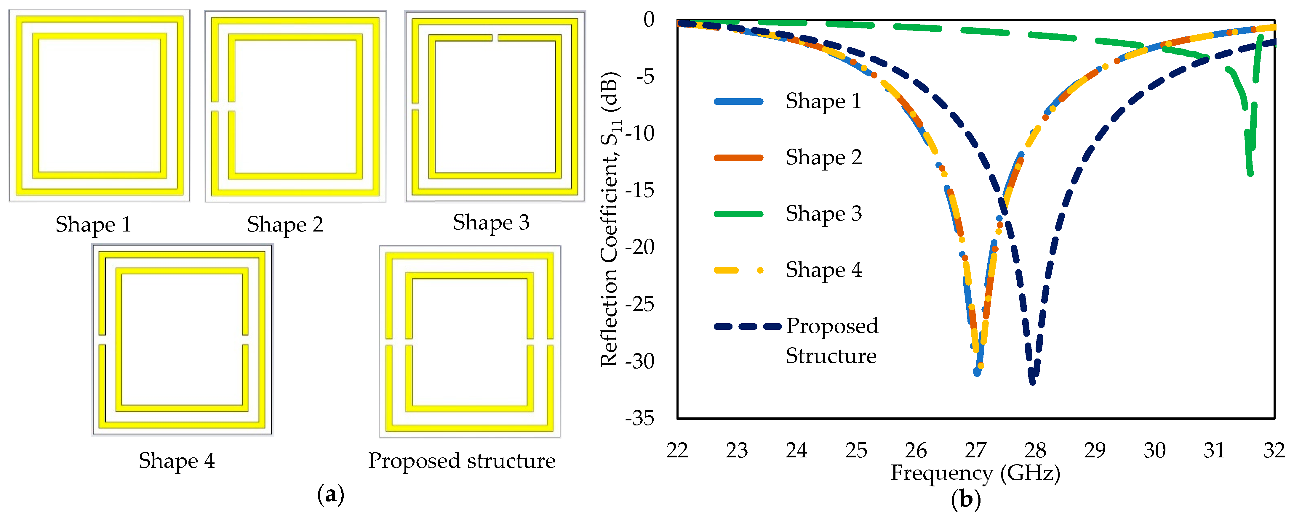
Before obtaining the final design of the unit cell, a study was conducted on a few ring resonators by keeping the area the same. All the shapes are 3.05 mm wide and 2.85 mm long. Among all designs, only five are shown in Figure 2a, with one of them being the proposed unit cell. All the shapes are composed of two rectangular metal resonators separated by 0.215 mm distance. The unit cells are simulated using two waveguide ports on both sides of the z-axes [shown in Figure 1c]; PEC and PMC are defined along x-axis and y-axis, respectively. The frequency responses ( S 11 ) of different designs are shown in Figure 2b. Shape 1 consists of two conventional resonators without any splits and resonates at 26.8 GHz (black dotted curve in the figure). From Equation (10), it is obvious that a decrease in inductance/capacitance would shift the resonance to the higher frequency. Slits are introduced in each resonator to move the resonance to the higher frequency to 27 GHz. Shape 3 consists of the same split in each resonator but 90° apart. The inner ring is placed 90° from the outer one to create mutual coupling so that the resonance shifts to the higher frequency. Figure 2b shows that the structure operates at 31.3 GHz (which is above the desired 28 GHz 5G band). Shape 4 contains two single-split resonators that operate at 26.82 GHz placed 180° apart. Eventually the proposed shape contains two splits in both resonators with optimum coupling between the resonators to operate at 28 GHz (green dotted line in the figure) with a −10 dB bandwidth of around 2 GHz.
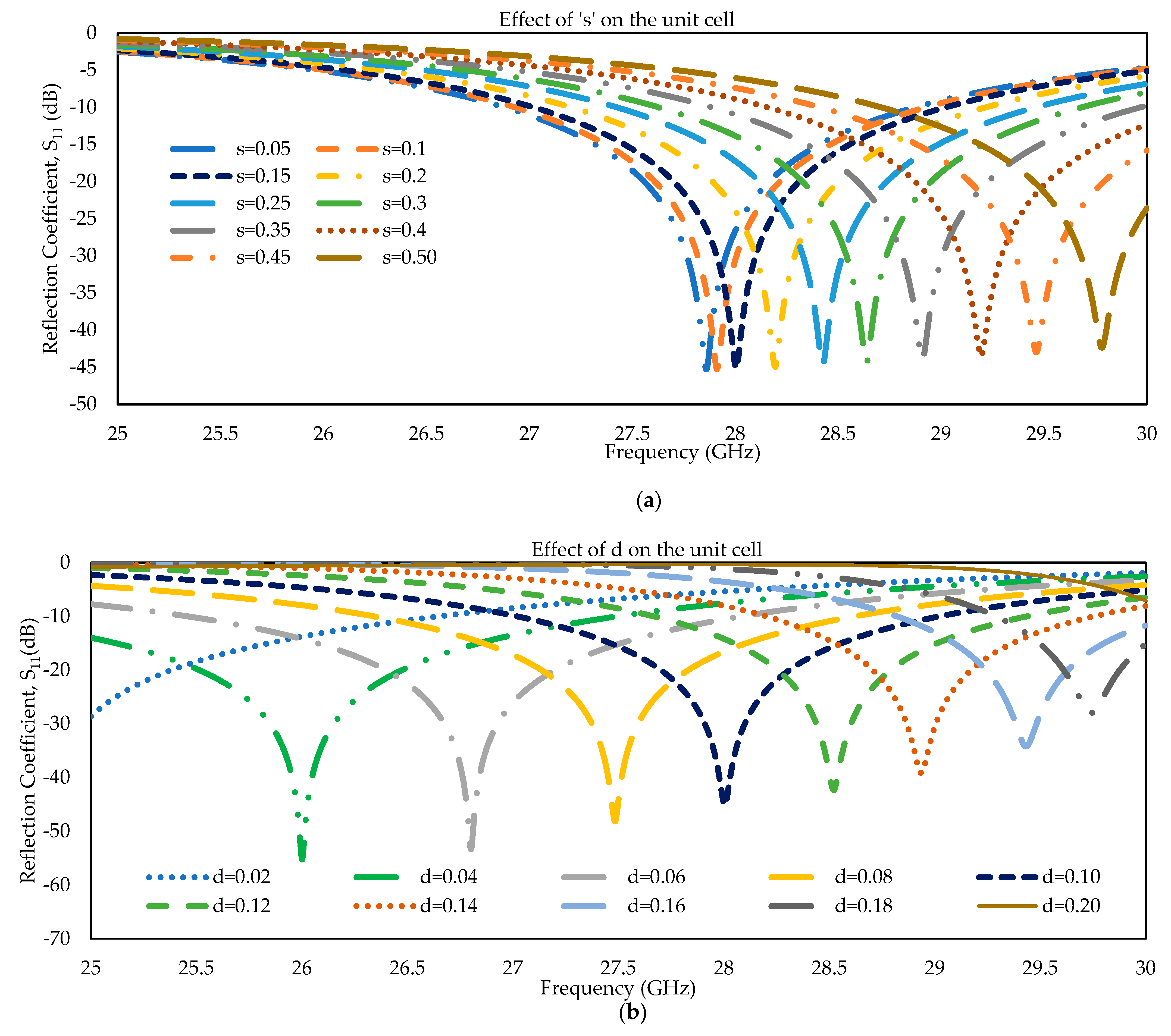
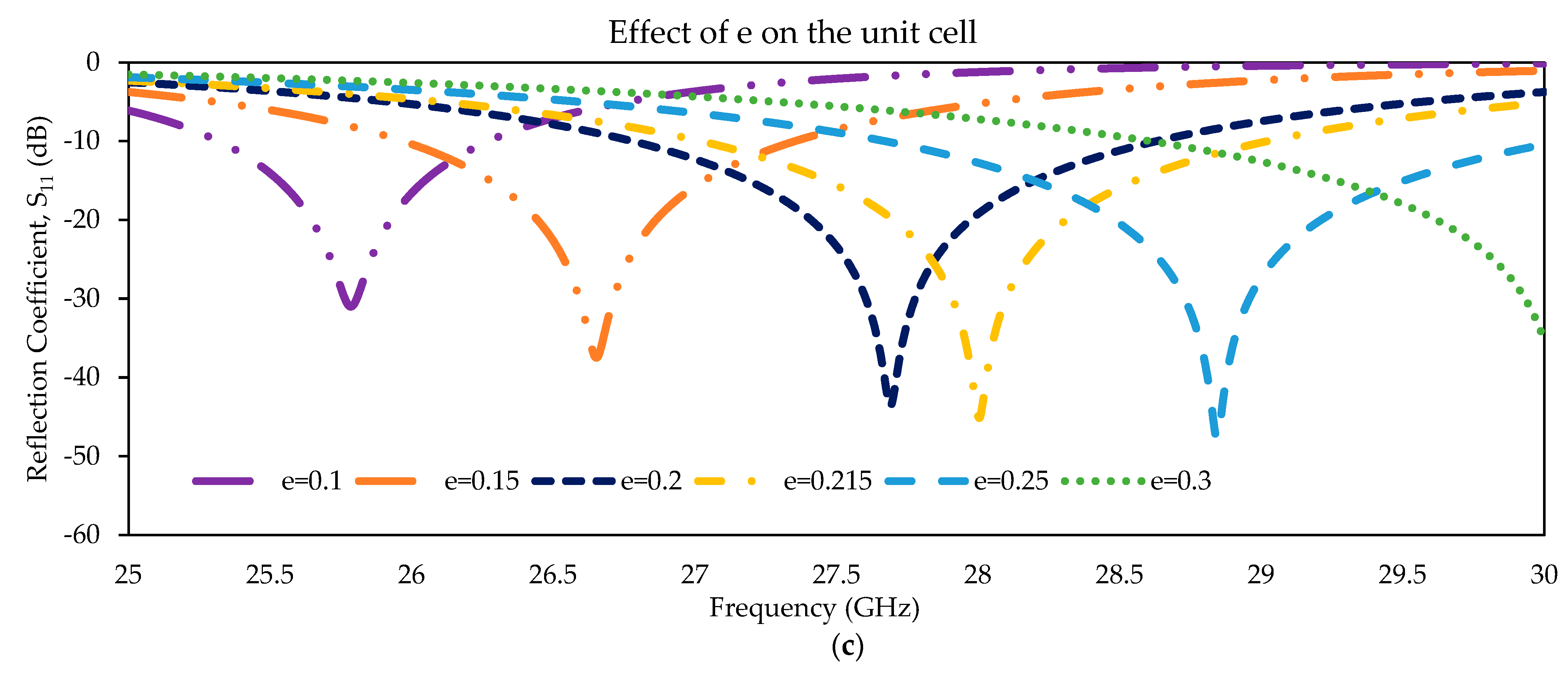
A parametric study of the proposed unit cell is conducted for the splits (denoted by ‘s’), width of the metal strips (denoted by ‘d’), and the distance between the resonators (denoted by ‘e’). It is evident from Figure 3 that these three parameters have significant impact on the structure to regulate its resonance frequency. Figure 3a exhibits the impact of splits on the resonance. When the split varies from 0.05 to 0.50 mm, the resonance frequency shifts from the lower frequency to the higher one. The structure operates at 28 GHz when the split is 0.15 mm wide.
Figure 3b shows the effect of metal strips’ width on regulating the resonance frequency. As the width of the metal strip varies from 0.01 to 0.20 mm, the resonance shifts from lower to higher frequency. The change in the gap helps regulate the mutual coupling between the resonators to control the resonance frequency. The structure exhibits resonance at 28 GHz with a bandwidth of around 2 GHz.
The distance between the resonators/rings is quite significant for the unit cell resonance. Figure 3c shows the response of the structure for various ‘e’ values. As the distance between the rings varies from 0.10 to 0.30 mm, the resonance shifts from lower to higher frequency.

4. Results

Figure 4a shows the reflection coefficient ( S 11 ) and transmission coefficient ( S 21 ) of the optimized unit cell, and Figure 4b shows the magnitude and phase behavior. It exhibits a −10 dB S 11 bandwidth of more than 2 GHz. The phase curve of the reflected wave crosses 0° at 28 GHz, at which the magnitude of S 11 is minimum (−38.73 dB).
This zero-reflection phase incidence indicates that the structure would be a great candidate for metamaterial/metasurface applications at 28 GHz.
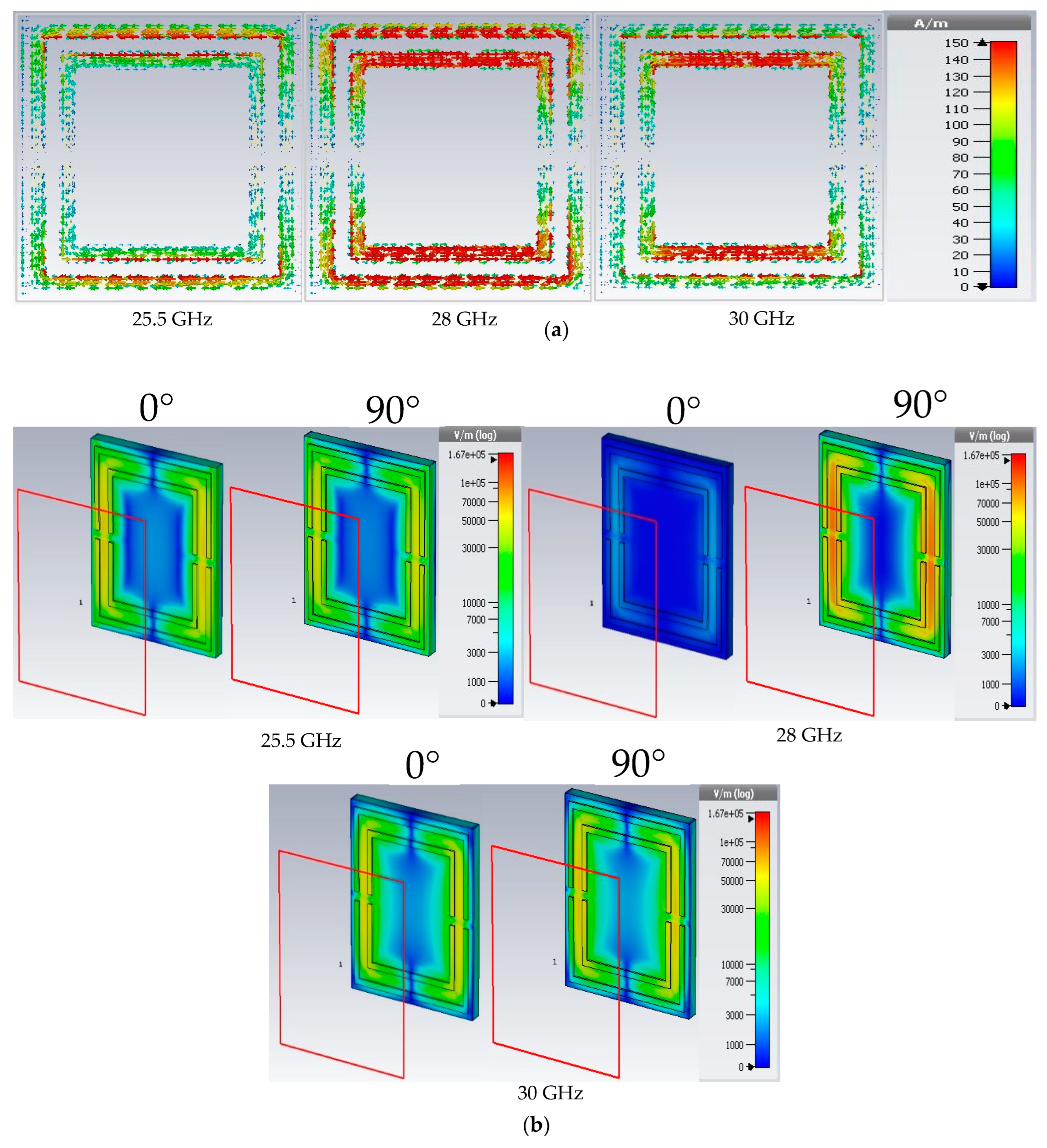
Figure 5a–c shows the current distribution, electric field, and magnetic field responses of the unit cell at 25.5 GHz, 28 GHz, and 30 GHz. The observation is made at two non-resonant frequencies along with the resonance frequency to understand the behavior of the unit cell. The surface current (electrical current) is predominant on the rings/metal strips. Current flows through the conducting surface of the structure more than any other fundamental parts of the structure. The splits of the rings regulate the current to rotate in the same direction in the same ring, causing passband behavior at the resonance frequency. It is evident from Figure 5a that the current density at 28 GHz is much higher than that at other non-resonant frequencies.
Due to the propagation of a homogenous wave along the X-axis, polarization occurs on the z-axis of the unit cell. As a result, a magnetic dipole in the y-direction is created because of the electric field in the x-direction, and an electric dipole in the x-direction is created because of the magnetic field in the y-direction [26]. The overall impact of these parameters is shown with color maps in Figure 5b and Figure 5c, respectively.
Figure 5b shows the electric field response, and Figure 5c shows the magnetic field phase response (0° and 90°) of the unit cell at 25.5, 28, and 30 GHz, respectively. It is obvious from Figure 5b that the electric field response of the unit cell at 28 GHz is higher than that at 25.5 and 30 GHz (non-resonance frequencies). However, the response is intense when the wave is being propagated at the 90° phase on the structure, which satisfies the condition of Maxwell’s equation where the surface current must be in-phase with the magnetic response and should be opposite to the electric field. Figure 5c confirms that the magnetic response is in-phase with the current flowing through the structure at 28 GHz, where it shows near-zero response at 90°.
The splits or gaps in the structure are considered as capacitors since they store energy in the form of electric fields. As a result, the combination of a dielectric response and an electrical resonance forms permittivity. Initially the fundamental energy of this ring resonator is stored as a magnetic field. This creates a magnetic resonance and combines with the dielectric response to create permeability. The electric field creates a magnetic dipole moment of the structure leading to form an artificial magnetism which turns out to be an effective negative permeability. Similarly, effective negative permittivity is created by the combination of magnetic and electric resonance. This imbrication carries out to be the effective negative refractive index of this metamaterial.
Figure 5d exhibits the behavior of the effective dielectric parameters of the structure over the frequency of operation by using the NRW method. It can be seen from the figure that the structure shows negative values for all the effective dielectric parameters, which makes the structure double-negative (DNG) metamaterial. Table 2 shows the frequency range of the effective dielectric parameters.

5. Array Configuration

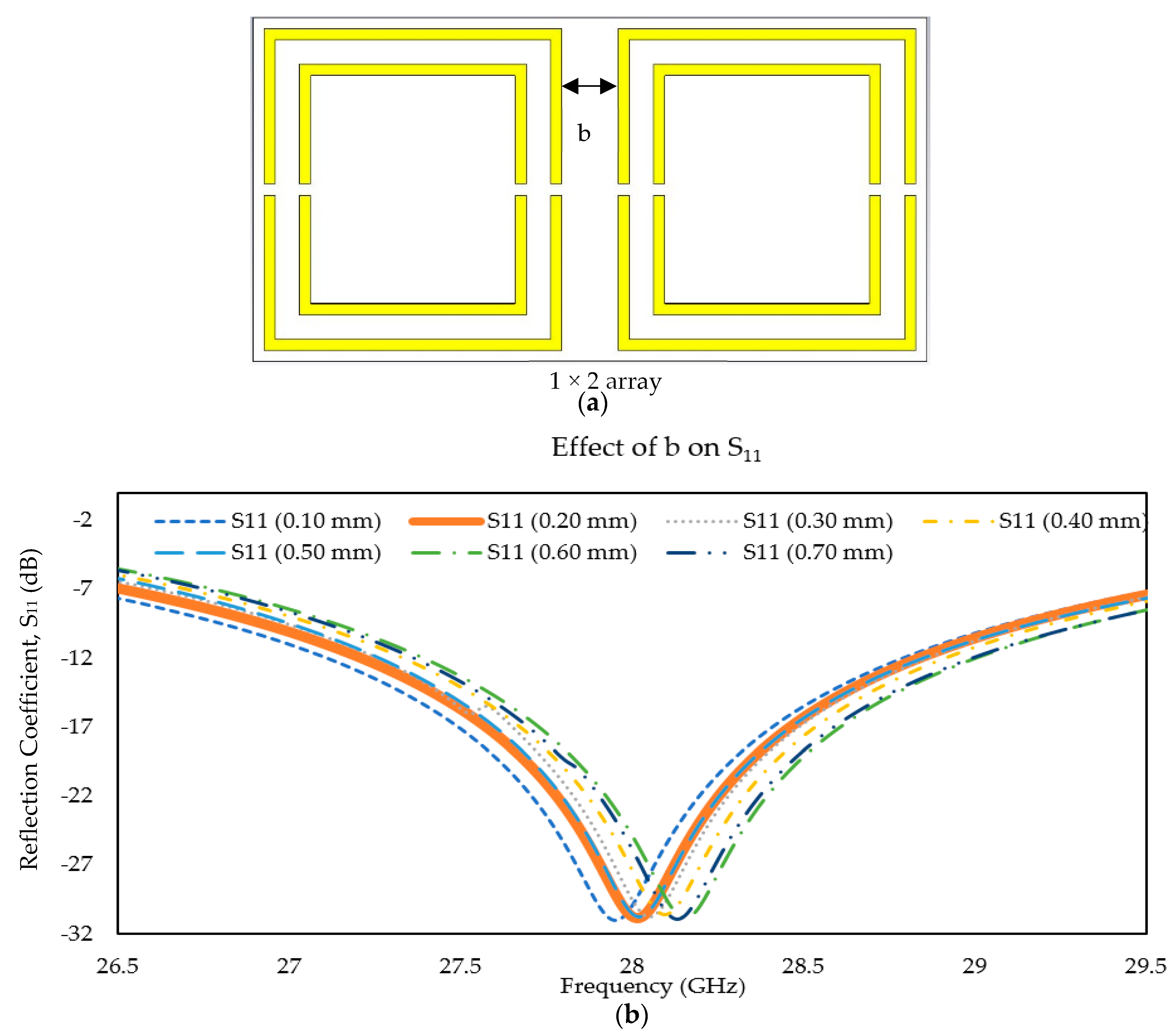
A comparative study is made on 1 × 2, 2 × 2, and 4 × 4 array configurations to validate the unit cell structure. Figure 6a shows the configuration of the 1 × 2 array where two unit cells are placed 0.20 mm (denoted by ‘b’) apart. Figure 6b shows the parametric study to determine the optimum distance for the unit cells. The study is performed for the distance from 0.10 mm to 0.70 mm, where the structure shows resonance at 28 GHz at 0.20 mm and 0.50 mm distance. However, the distance between the units is selected as b = 0.20 mm to make the overall structure compact, and at this distance (0.20 mm) the structure exhibits slightly higher bandwidth than that at 0.50 mm.
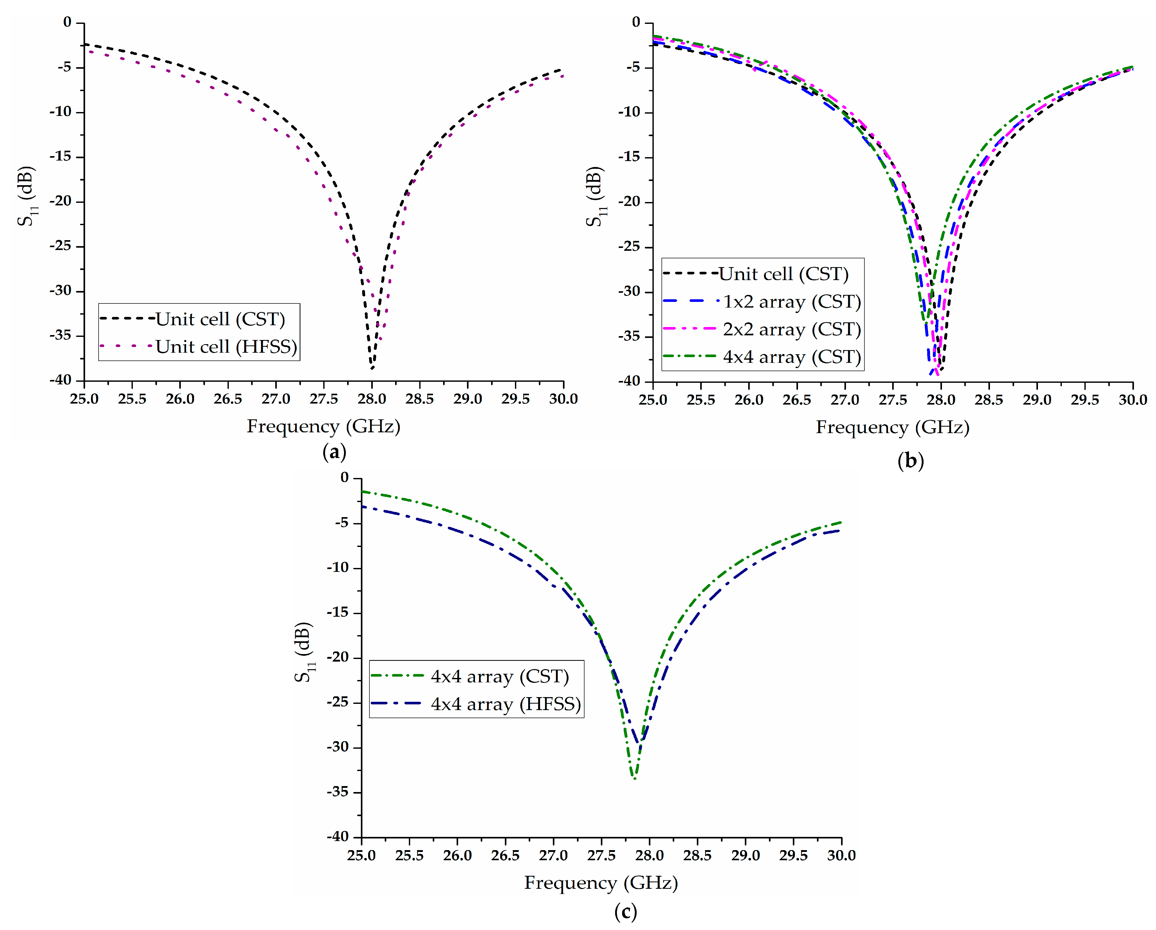
The same process is followed to design 2 × 2 and 4 × 4 arrays. The S 11 magnitude of these arrays with the unit cell is shown in Figure 7a. All the arrays operate at 28 GHz indicating the accuracy of the unit cell simulations. The unit cell and 4 × 4 array configurations are further simulated in finite-element-method (FEM)-based high-frequency simulation software (HFSS) to validate its result. The result from HFSS shows good agreement with those obtained from CST. This study also confirms that arrays of this unit cell can be used in developing metamaterial-based FSSs, electromagnetic absorbers, filters, super lenses, etc.

6. Effective Dielectric Parameter Analysis of the Arrays

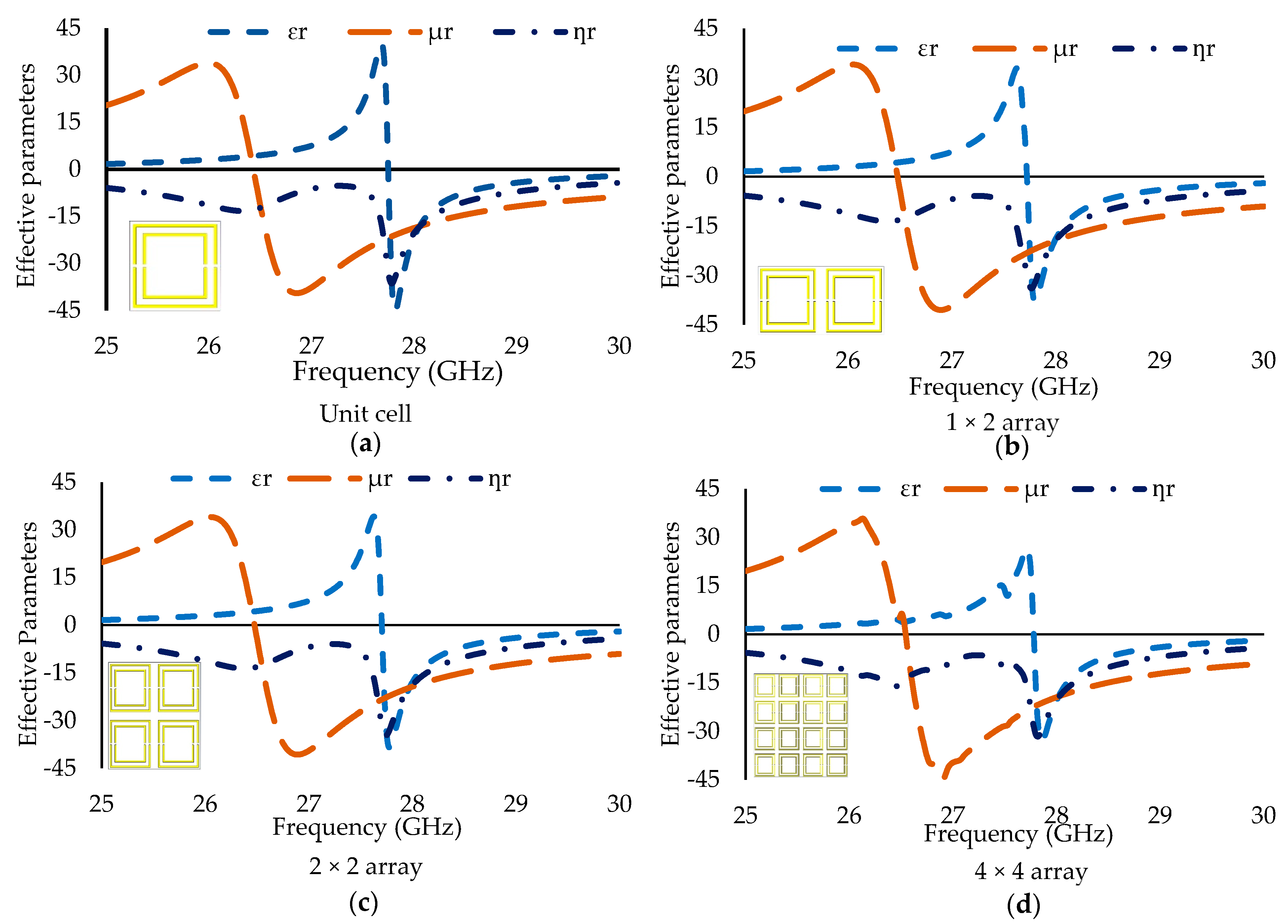
Figure 8 shows a comparative analysis of effective dielectric parameters between unit cell and array configurations. Similar NRW and direct retrieval methods are used to extract the values of these parameters. Figure 8 shows the results within the frequency range of 25 to 30 GHz, where the structure exhibits DNG properties for all the configurations. The unit cell shows negative effective permittivity (within 25 to 30 GHz) from 27.475 GHz to 30 GHz with a minimum value of −48.22. The array configurations follow the trend of the unit structure with a slight shift in frequencies. In the case of the 1 × 2 array, the range is from 27.725 to 30 GHz, with a minimum value (PMV) of −38.10; for the 2 × 2 array, the range is from 27.705 to 30 GHz, with a PMV of −38.55; and for the 4 × 4 array, it is from 27.78 to 30 GHz, with a PMV of 33.20. The arrays exhibit similar agreement in other effective dielectric parameters (effective permeability and refractive index). Table 3 summarizes these parameters for different arrays. It is evident from Table 3 that all the configurations show negative values of the effective dielectric parameters within the frequency range of 25 to 30 GHz (including the resonance frequency), which further validates that the structure is a DNG metamaterial at 5G mmWave frequency (28 GHz).
Esmail et al. [3] have proposed a process to reconfigure the radiation pattern of planar antennas using metamaterial for 5G applications. The size of the unit cell is 3.3 × 3.2 mm2, where the operating frequency of the structure is 28.95 GHz. The single-layered structure is developed on a Rogers RT/duroid 5880 substrate with a thickness of 0.254 mm. Khalili et al. [28] have proposed a 1.4 × 1.4 mm2 unit cell operating at 30 GHz to achieve a very good isolation between the output ports of a millimeter-wave power divider (MWPD). Both these unit cells are developed to resonate at 5G mmWave frequency. However, neither of these cells is focused on 28 GHz, and they are being used to improve the performance of the antenna. El-Nady et al. [29] have proposed an Epsilon-near-zero (ENZ) metamaterial for 5G applications. The 2.5 × 2.5 mm2 unit cell is on a comparatively thicker substrate RT 6035 with a thickness of 0.508 mm. Naqvi et al. [30] have recently proposed an 8 × 8 mm2 metamaterial absorber that can be used for 24 GHz and 28 GHz applications. Nevertheless, the structure is developed on a thicker FR-4 substrate, and the size of the unit cell is bigger than our proposed work. Al-Bawri et al. [31] presented a single-layered hexagonal-shaped near-zero-index (NZI) metamaterial-based mimo antenna for mmWave applications. The 4 × 4 mm2 unit cell was developed on a 0.787 mm thick Rogers RT 5880 substrate, where the structure has a wide negative range of single mu metamaterial (MNG). All the metamaterial unit cells mentioned above are highly effective in their particular applications, but none of them has reported the DNG characteristic at the resonance frequencies. Most of the unit cells mentioned in this discussion are either bigger in size or developed in a thicker substrate, which makes the proposed structure unique from the rest. The comparison of the proposed structure with the existing works is shown in Table 4.

7. Conclusions

In this article, double-negative rectangular metamaterial unit structure at 5G mmWave frequency was designed and studied. Rogers RT/Duroid 5880 as substrate material and conventional copper clay as conductive path were used to model the structure. The performance of the structure was simulated on CST simulation software, where the NRW approach was used to retrieve the metamaterial properties. Different array configurations were developed to verify the performance of the unit cell. The results were confirmed by Ansys HFSS simulation software. Negative values of the effective dielectric parameters and the plots of scattering parameters of various array configurations at 28 GHz confirmed that the proposed metamaterial structure is suitable for mmWave 5G applications. The unit cell exhibits a 2 GHz bandwidth of operation and can be used to develop mmWave-frequency-selective surfaces, antennas, absorbers, or filters.

Author Contributions

Conceptualization, M.J.A. and S.I.L.; methodology, M.J.A..; software, M.J.A.; validation, M.J.A., and S.I.L.; formal analysis, M.J.A.; investigation, M.J.A.; resources, S.I.L.; data curation, M.J.A.; writing—original draft preparation, M.J.A.; writing—review and editing, M.J.A. and S.I.L.; visualization, M.J.A.; supervision, S.I.L.; project administration, S.I.L.; funding acquisition, S.I.L. All authors have read and agreed to the published version of the manuscript.

Funding

The project was partially funded by the National Science Foundation (Award Number: 1833016) and the Alabama Commission on Higher Education (ACHE).

Data Availability Statement

Data is unavailable due to privacy.

Acknowledgments

The authors would like to acknowledge the support provided by the National Science Foundation (Award Number: 1833016) and the Alabama Commission on Higher Education (ACHE) for partially funding this project.

Conflicts of Interest

The authors declare no conflict of interest.

References

  1. Esmail, B.A.; Majid, H.A.; Dahlan, S.H.; Zainal Abidin, Z.; Himdi, M.; Dewan, R.; Rahim, M.K.; Ashyap, A.Y. Reconfigurable metamaterial structure for 5G beam tilting antenna applications. Waves Random Complex Media 2021, 31, 2089–2102. [Google Scholar] [CrossRef]
  2. Wani, Z.; Abegaonkar, M.P.; Koul, S.K. A 28-GHz antenna for 5G MIMO applications. Prog. Electromagn. Res. Lett. 2018, 78, 73–79. [Google Scholar] [CrossRef] [Green Version]
  3. Esmail, B.A.; Majid, H.A.; Abidin, Z.Z.; Dahlan, S.H.; Himdi, M.; Dewan, R.; Rahim, M.K.A.; Al-Fadhali, N. Reconfigurable Radiation Pattern of Planar Antenna Using Metamaterial for 5G Applications. Materials 2020, 13, 582. [Google Scholar] [CrossRef] [PubMed] [Green Version]
  4. Rappaport, T.S.; Sun, S.; Mayzus, R.; Zhao, H.; Azar, Y.; Wang, K.; Wong, G.N.; Schulz, J.K.; Samimi, M.; Gutierrez, F. Millimeter wave mobile communications for 5G cellular: It will work! IEEE Access 2013, 1, 335–349. [Google Scholar] [CrossRef]
  5. Sulyman, A.I.; Nassar, A.T.; Samimi, M.K.; MacCartney, G.R.; Rappaport, T.S.; Alsanie, A. Radio propagation path loss models for 5G cellular networks in the 28 GHz and 38 GHz milli-meter-wave bands. IEEE Commun. Mag. 2014, 52, 78–86. [Google Scholar] [CrossRef]
  6. Connect America Fund. Report and Order and Further Notice of Proposed Rulemaking; Federal Communications Commission: Washington, DC, USA, 2011; pp. 10–90. [Google Scholar]
  7. Zhang, Y.P.; Liu, D. Antenna-on-chip and antenna-in-package solutions to highly integrated millime-ter-wave devices for wireless communications. IEEE Trans. Antennas Propag. 2009, 57, 2830–2841. [Google Scholar] [CrossRef]
  8. Zhang, Y.P.; Sun, M.; Chua, K.M.; Wai, L.L.; Liu, D. Antenna-in-package design for wirebond inter-connection to highly integrated 60-GHz radios. IEEE Trans. Antennas Propag. 2009, 57, 2842–2852. [Google Scholar] [CrossRef]
  9. Karim, R.; Iftikhar, A.; Ramzan, R. Performance-Issues-Mitigation-Techniques for On-Chip-Antennas–Recent Developments in RF, MM-Wave, and THz Bands with Future Directions. IEEE Access 2020, 8, 219577–219610. [Google Scholar] [CrossRef]
  10. Karim, R.; Iftikhar, A.; Ijaz, B.; Mabrouk, I.B. The potentials, challenges, and future directions of on-chip-antennas for emerging wireless applications—A comprehensive survey. IEEE Access 2019, 7, 173897–173934. [Google Scholar] [CrossRef]
  11. Alwareth, H.; Ibrahim, I.M.; Zakaria, Z.; Al-Gburi, A.J.A.; Ahmed, S.; Nasser, Z.A. A Wideband High-Gain Microstrip Array Antenna Integrated with Frequency-Selective Surface for Sub-6 GHz 5G Applications. Micromachines 2022, 13, 1215. [Google Scholar] [CrossRef]
  12. Xiong, J.; Yang, B.; Wu, Y.; Zeng, X.; Li, Q.; Tang, R.; Lin, H. Broadband-Transmissive, Frequency-Selective Rasorber Design Using Characteristic Mode Analysis. Electronics 2022, 11, 1418. [Google Scholar] [CrossRef]
  13. Veselago, V.G. The Electrodynamics of Substances with Simultaneously Negative Values of ε and µ. Phys. Uspekhi 1968, 10, 509–514. [Google Scholar] [CrossRef]
  14. Smith, K.L.; Adams, R.S. Spherical Spiral Metamaterial Unit Cell for Negative Permeability and Negative Permittivity. IEEE Trans. Antennas Propag. 2018, 66, 6425–6428. [Google Scholar] [CrossRef]
  15. Alam, J.; Ahamed, E.; Faruque, M.R.I.; Islam, M.T.; Tamim, A.M. Left-handed metamaterial bandpass filter for GPS, Earth Exploration-Satellite and WiMAX frequency sensing applications. PLoS ONE 2019, 14, e0224478. [Google Scholar] [CrossRef]
  16. Suzuki, T.; Harumi, A. Reflectionless zero refractive index metasurface in the terahertz waveband. Opt. Express 2020, 28, 21509–21521. [Google Scholar] [CrossRef]
  17. Islam, S.S.; Faruque, M.R.I.; Islam, M.T. An Object-Independent ENZ Metamaterial-Based Wideband Electromagnetic Cloak. Sci. Rep. 2016, 6, 33624. [Google Scholar] [CrossRef] [Green Version]
  18. Hossain, M.J.; Faruque, M.R.I.; Islam, M.T. Correction: Perfect metamaterial absorber with high fractional bandwidth for solar energy harvesting. PLoS ONE 2019, 14, e0211751. [Google Scholar] [CrossRef] [Green Version]
  19. Emadi, R.; Reza, S.A.; Zeidaabadi, N. Plasmonic cloaking for irregular inclusions using an epsilon-near-zero region composed of a graphene-silica stack. JOSA B 2018, 35, 643–651. [Google Scholar] [CrossRef]
  20. Islam, S.S.; Faruque, M.R.I.; Islam, M.T. The Design and Analysis of a Novel Split-H-Shaped Metamaterial for Multi-Band Microwave Applications. Materials 2014, 7, 4994–5011. [Google Scholar] [CrossRef] [Green Version]
  21. Hossain, I.; Faruque, M.R.I.; Islam, M.T.; Ullah, M.H. A New Wide-Band Double-Negative Metamaterial for C- and S-Band Applications. Materials 2014, 8, 57–71. [Google Scholar] [CrossRef]
  22. Alam, T.; Faruque, M.R.I.; Islam, M.T. A double-negative metamateri-al-inspired mobile wireless antenna for electromagnetic absorption reduction. Materials 2015, 8, 4817–4828. [Google Scholar] [CrossRef] [PubMed] [Green Version]
  23. Hasan, M.; Faruque, M.R.I.; Islam, S.S.; Islam, M.T. A New Compact Double-Negative Miniaturized Metamaterial for Wideband Operation. Materials 2016, 9, 830. [Google Scholar] [CrossRef] [PubMed] [Green Version]
  24. Islam, S.S.; Khan, M.S.; Faruque, M.R.I. Design and analysis of modified-split-H-shaped DNG metamaterial for microwave application. Mater. Res. Express 2020, 6, 125808. [Google Scholar] [CrossRef]
  25. Alam, J.; Faruque, M.R.I.; Islam, M.T. Labyrinth double split open loop resonator based bandpass filter design for S, C and X-band application. J. Phys. D Appl. Phys. 2018, 51, 265102. [Google Scholar] [CrossRef]
  26. Tamim, A.M.; Faruque, M.R.I.; Alam, M.J.; Islam, S.S.; Islam, M.T. Split ring resonator loaded horizontally inverse double L-shaped metamaterial for C-, X-and Ku-Band Microwave applications. Results Phys. 2019, 12, 2112–2122. [Google Scholar] [CrossRef]
  27. Nicolson, A.M.; Ross, G.F. Measurement of the Intrinsic Properties of Materials by Time-Domain Techniques. IEEE Trans. Instrum. Meas. 1970, 19, 377–382. [Google Scholar] [CrossRef] [Green Version]
  28. Khajeh-Khalili, F.; Honarvar, M.A.; Limiti, E. A novel high-isolation resistor-less millimeter-wave power divider based on metamaterial structures for 5G applications. IEEE Trans. Compon. Packag. Manuf. Technol. 2020, 11, 294–301. [Google Scholar] [CrossRef]
  29. El-Nady, S.; Elsharkawy, R.R.; Afifi, A.I.; El-Hameed, A.S.A. Performance Improvement of Substrate Integrated Cavity Fed Dipole Array Antenna Using ENZ Metamaterial for 5G Applications. Sensors 2021, 22, 125. [Google Scholar] [CrossRef]
  30. Naqvi, S.A.; Baqir, M.A.; Gourley, G.; Iftikhar, A.; Khan, M.S.; Anagnostou, D.E. A Novel Meander Line Metamaterial Absorber Operating at 24 GHz and 28 GHz for the 5G Applications. Sensors 2022, 22, 3764. [Google Scholar] [CrossRef]
  31. Al-Bawri, S.S.; Islam, M.T.; Shabbir, T.; Muhammad, G.; Islam, S.; Wong, H.Y. Hexagonal Shaped Near Zero Index (NZI) Metamaterial Based MIMO Antenna for Millimeter-Wave Application. IEEE Access 2020, 8, 181003–181013. [Google Scholar] [CrossRef]
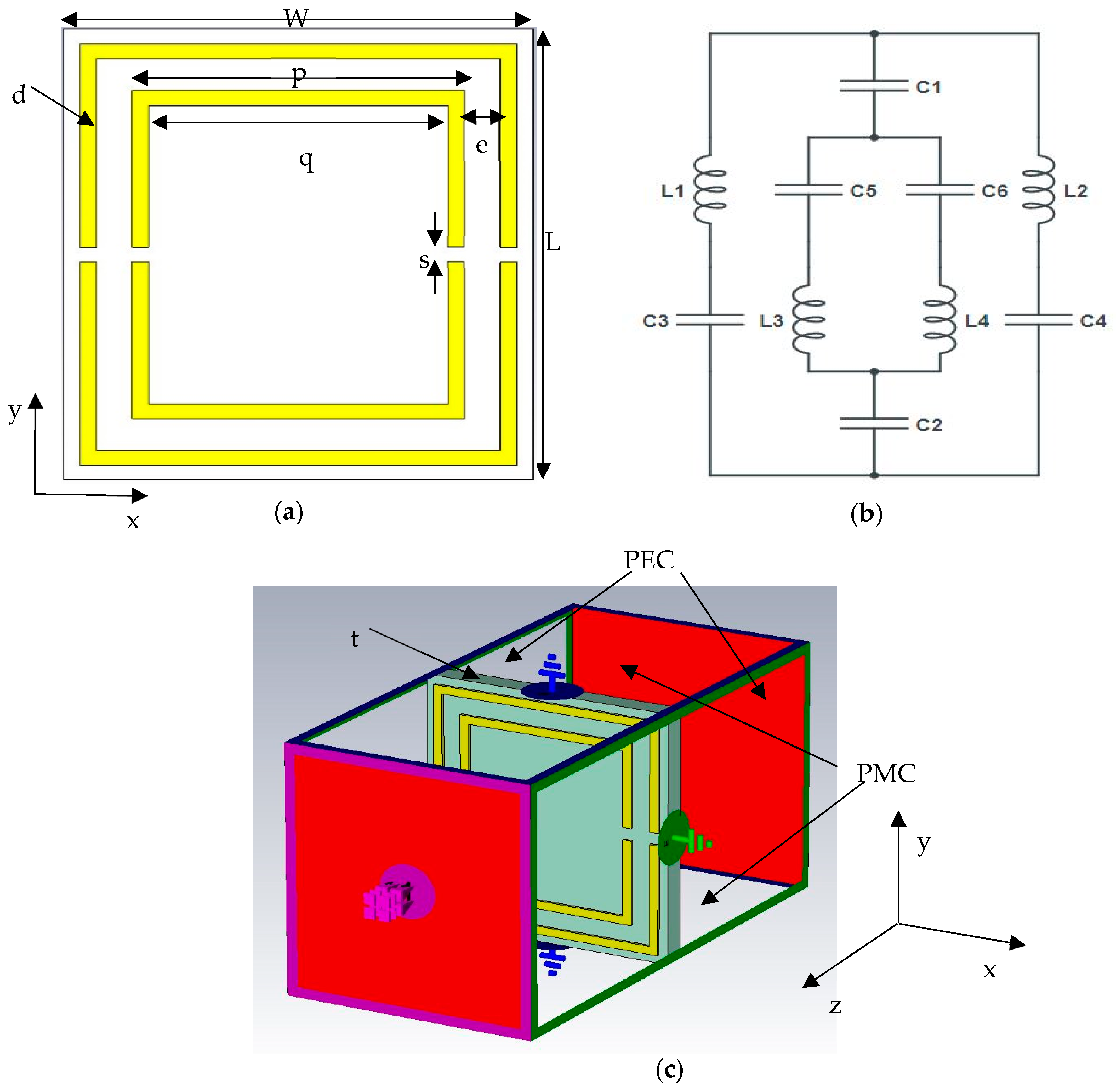
Figure 1. (a) Schematic diagram showing the geometry of the structure, (b) equivalent circuit, and (c) prospective view of the unit cell exhibiting simulation set up with boundary conditions.
Electronics 12 00174 g001
Figure 2. (a) Development of unit cell, (b) reflection coefficient, S 11 (dB) response of different unit structure.
Electronics 12 00174 g002
Figure 3. (ac) Effect of ‘s’, ‘d’ and ‘e’ on the magnetic resonance.
Electronics 12 00174 g003aElectronics 12 00174 g003b
Figure 4. (a) Reflection coefficient ( S 11 ) and transmission coefficient ( S 21 ) vs. frequency, (b) S 11 magnitude, and phase of the structure.
Electronics 12 00174 g004
Figure 5. (a) Current distribution, (b) electric field, (c) magnetic field response at 25.5 GHz, 28 GHz, and 30 GHz and (d) effective dielectric parameters of the unit cell at 28 GHz.
Electronics 12 00174 g005aElectronics 12 00174 g005b
Figure 6. (a) 2 × 1 array formation and (b) effect of distance of the unit cells on the resonance.
Electronics 12 00174 g006
Figure 7. Validation of s-parameters: (a) Unit cell comparison between CST and HFSS, (b) different array configurations of the structure, (c) 4 × 4 array comparison between CST and HFSS.
Electronics 12 00174 g007
Figure 8. Negative effective parameters of (a) unit cell, (b) 1 × 2 array, (c) 2 × 2 array, and (d) 4 × 4 array formations.
Electronics 12 00174 g008
Table 1. Dimensions of the unit cell.
ParametersMeasurement (mm)
W2.85
L3.05
p2.22
q2.02
d0.1
e0.215
s0.15
t0.254
b0.2
Table 2. Frequency region of effective dielectric parameters of the developed unit structure.
ParametersFreq. Range (GHz)Negative Index At 28 GHz
Effective Permittivity27.475–30−10.60
Effective Permeability26.37–30−18.68
Effective Refractive Index25–30−14.082
Double Negative region27.475–30−10.60 & −18.68
Table 3. Frequency range of negative effective dielectric parameters of the unit structure and different arrays.
StructureParametersFrequency Range (GHz)Peak Minimum ValuesValues at 28 GHzDNG Region (GHz)
Unit cellPermittivity27.475–30 (BW of 2.525)−48.22−10.6027.475–30 (BW of 2.525)
Permeability26.37–30 (BW of 3.63)−44.39−18.68
Refractive index25–30 (BW of 5)−41.50−14.08
1 × 2 arrayPermittivity27.725–30 (BW of 2.275)−38.10−18.7927.725–30 (BW of 2.275)
Permeability26.48–30 (BW of 3.52)−40.54−19.3609
Refractive index25–30 (BW of 5)−33.96−19.2519
2 × 2 arrayPermittivity27.705–30 (BW of 2.295)−38.55−17.9327.705–30 (BW of 2.295)
Permeability26.475–30 (BW of 3.525)−40.67−19.36
Refractive index25–30 (BW of 5)−34.73−18.79
4 × 4 arrayPermittivity27.78–30 (BW of 2.22)−33.20−20.557927.78–30 (BW of 2.22)
Permeability26.545–30 (BW of 3.455)−44.85−19.5076
Refractive index25–30 (BW of 5)−31.63−20.3937
Table 4. Comparison of the proposed DNG metamaterial with previous works.
Previous WorksFreq. Band (GHz)Size (mm2)Type of Substrate (Thickness)Metallic Layer
Esmail et al. (2020) [3]28.7–29.23.3 × 3.2RT-5880 (0.254 mm)one
Khalili et al. (2021) [28]28.0–32.01.4 × 1.4RT-5880 (0.254 mm)one
El-Nady et al. (2021) [29]28.5–30.52.5 × 2.5RT-6035 (0.508 mm)one
Naqvi et al. (2022) [30]24.25–24.45 & 27.5–28.358.0 × 8.0FR-4 (1.6 mm)one
Al-Bawri et al. (2020) [31]26.4–29.1 4.0 × 4.0RT-5880 (0.787 mm)one
Proposed Work27.1–29.23.05 × 2.85RT-5880 (0.254 mm)one
Disclaimer/Publisher’s Note: The statements, opinions and data contained in all publications are solely those of the individual author(s) and contributor(s) and not of MDPI and/or the editor(s). MDPI and/or the editor(s) disclaim responsibility for any injury to people or property resulting from any ideas, methods, instructions or products referred to in the content.