1. Introduction
As one of the new types of wide bandgap semiconductor devices, GaN high electron mobility devices have lower conduction resistance, smaller junction capacitance, faster switching frequency, and strong temperature resistance ability, as the power devices for motor drives are expected to improve the highest working frequency and efficiency, and in the meantime reduce the volume and weight [
1,
2,
3,
4]. Thus, it has very broad range of application scenarios for high-speed motor drives, servo drives, electric vehicles, etc.
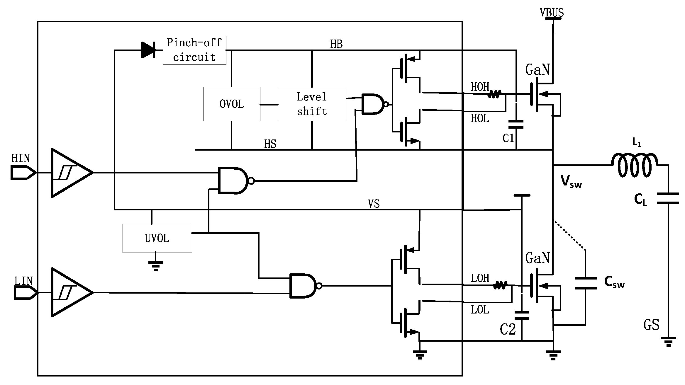
When the GaN device is applied to the half bridge topology of the motor driver shown in
Figure 1, the insertion dead-time can avoid the bridge arm straight-through situation. However, GaN_FET exhibit a larger reverse conduction drop V
SD and loss P due to the lack of a body diode, which will affect the efficiency of the system significantly. I
SD is the source-drain current, F
S is operating frequency, and T
conv is reverse conduction time [
5,
6,
7,
8].
Researchers have carried out relevant studies on dead-time optimization settings. Xue J et al. discuss the reverse conduction loss when dead-time is excessive [
9]; Zhang Yi et al. discuss the switch loss caused by output capacitance when dead-time is insufficient [
7]. Therefore, the best dead-time is that which can not only avoid the switching loss but also reverse conduction loss. If a low-side GaN transistor turned on after V
sw becomes 0 V and a high-side power transistor turned on after V
sw becomes V
BUS, the switching loss can be eliminated. This switching mode mentioned above is called zero voltage switching (ZVS). Hong Y U et al. propose a scheme which is based on detection of switching node voltage and feedback to the gate of the power transistor [
10], but this scheme needs a low delay level shift circuit, otherwise it will produce excessive dead-time. Cheng Q et al. designed a dead-time circuit based on detecting load-side current passing through an appropriate delay drive transistor, but it is not suitable for a wide load range or high voltage applications [
11]. Xue J et al. carried out design of a dead-time circuit structure based on detecting the drain-source voltage of a power transistor [
9], in which the small detection delay enables the circuit to work under MHz, but it may lead to switching loss. Xugang Ke et al. completed a GaN driver with active BST balance and Vsw dual-edge dead-time modulation, achieving 8.3% efficiency improvement and 3.4 ns constant propagation delay [
12], but its maximum voltage level is 40 V.
Based on the realization of ZVS, the reverse conduction time should be reduced as much as possible to achieve the purpose of reducing the reverse conduction loss by generating appropriate delay according to different load conditions, which can improve the efficiency of the drive circuit. For different load conditions, the slew rate of switch node V
sw dissimilates. So, the optimal dead-time T
opt should change along with load conditions.
In this formula,
is the capacitance of the switch node at the connection point of high and low power transistors,
is bus voltage,
Io is load current. The ideal switching conditions of high- and low-side transistors under different load conditions are shown in
Figure 2.
To realize ZVS, GaN transistors should turn on when the source-drain voltage drops near to zero. To reduce reverse conduction loss, GaN transistors’ turn-on should not be too late after its source-drain voltage drops near to zero. So, this paper proposes an adaptive dead-time control circuit for a maximum work frequency of 20 MHz, maximum voltage level 90 V GaN gate driver, which dissipates 56.3 uA quiescent current and is able to provide maximum 5 ns dead-time error for GaN gate driver.
2. Circuit Structure
The adaptive dead-time circuit proposed in this paper is based on GaN transistors’ drain-source voltage detection which belongs to the ipsilateral feedback control; this structure features low delay. The scheme is shown in
Figure 3. The adaptive dead-time control circuit includes a Source-Drain Voltage Sense circuit, Current Sense circuit and Delay circuit which can be divided into high-side and low-side. Both high-side and low-side input signal are generated by the forward level shift module in this paper. The subsequent drive module could reverse the V
OUTH and V
OUTL to V
GH and V
GL.
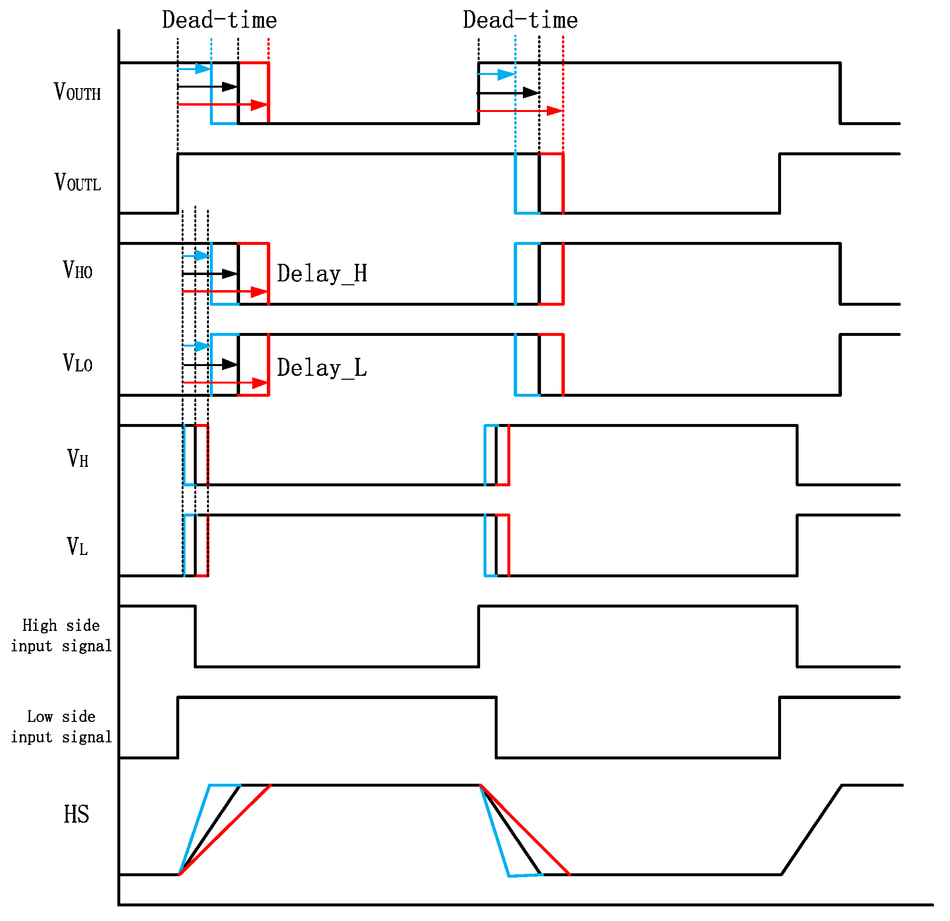
The working waveform is shown in
Figure 4, where Delay_H and Delay_L correspond to the delay generated by the high-side delay module and low-side delay module. Dead-time dissimilates along a different delay, V
H and V
L switch when HS starts to switch, and then pass through the delay module which is modulated by Current Sense. Finally, V
HO and V
LO ORing high-side input signal and low-side input signal to combine turn-on signal and turn-off signal. V
HO and V
LO provide the turn-on signal while the high-side input signal and low-side input signal provide the turn-off signal. In the meantime, there is a driver (composed of multiple step-step largened buffers to improve current load performance) which possess a delay of about 5 ns (this delay is unavoidable and limits the maximum operating frequency of the gate driver with proposed adaptive dead-time circuit); therefore, we could make V
OUTH and V
OUTL switch properly or slightly ahead of HS to become 0 V or V
BUS in the design of the delay module, and in this way we can reduce the reverse conduction time and maximize operating frequency.
2.1. Source-Drain Voltage Sense Circuit Design
In
Figure 5, the proposed Source-Drain Voltage Sense circuit in this paper is displayed. HS is the high-side ground and switch node, MN1 and MP5 are the high voltage LDMOS, and the EN signal works as the fault protection signal. Bipolar Q1 and Q2 clamp the voltage at OUTH and OUTL.
The high-side Source-Drain Sense is showed on the left of the figure; it detects the Source-Drain voltage drop of the high-side GaN transistor—the voltage drop falls when the GaN transistor enters the mill plateau of the turn-on process. MP1 and MN2 are constant turn-on MOSFET, and there is a resistance between MN1′s gate and drain which can make MN1 instantaneous turn-on during switching. The input signal of this sense is HS, and transforms the voltage signal into current signal during switching by LDMOS’s parasitism, and charge or discharge the upper plate of C1; in this way the current signal transforms into voltage signal at OUTH. When the low-side GaN transistor turns off, HS starts to rise for the freewheel current of external inductors; while the voltage drops between VBUS and HS start to fall, C1 starts to discharge from MN2 to MN2, as the charge between C1 cannot change groundless and MN1 is closed in the beginning, so the charge starts to charge the gate of MN1 through the resistance until MN1 turns on.
Subsequently, the voltage drops between the upper plate of C1 and HS falls, and this edge-of-fall works as the enable signal for the following part.
The low-side Source-Drain Sense showed on the right of the figure works in a similar way: when the high-side GaN transistor is turned off, HS starts to fall for the freewheel current of external inductors; while the voltage drop between HS and GS starts to fall, C2 starts to discharge from MN6 to MP5, for the charge between C2 cannot change groundless and MP5 is closed in the beginning, so the charge from HS starts to charge the gate of MP5 through the resistance until MP5 is turned on. Subsequently, the voltage drops between the upper plate of C2 and GS falls, and this edge-of-fall works as the enable signal for the following part. The Sense worked in low quiescent current for a normally closed design.
2.2. Current Sense Circuit Design
The Current Sense Circuit is showed in
Figure 6, which is similar to the Source-Drain Sense; the replication of current from VBUS to HS and HS to GS transforms into I
H and I
L. I
H and I
L are used to modulate the delay of the Delay module. It is worth noting that the current would change due to different load conditions (in gate driver means the fall or rise time of HS is different) which corresponds to adaptive adjustment.
2.3. Delay Circuit Design
In
Figure 7 and
Figure 8, we can see OUTH and OUTL are detected by the threshold of the inverter and modulate the delay by I
H and C
3 or I
L and C
4 into V
HO and V
LO.
The delay generated at C
3 can be expressed as T
1, and the delay generated at C
4 can be expressed as T
2.
While the C3, C4, , , , can be regarded as a fixed value, so the delay is only modulated by ISEN (, ). To make the delay sensitive only to ISEN, and must be insensitive to the supply, so a bias current souse is designed as follows.
To achieve a small delay deviation generated by the dead-time control circuit, a current source with low supply sensitivity is designed in
Figure 9. When the supply is on, MN22 turns on and provides bias for MN20 and MP17, and the current source starts to provide bias. This structure mainly takes advantage of the fact that MOS saturation current is only relative to overdrive voltage, and MOS resistance can adjust itself along with the current.
According to the above formula, it can be concluded that the current and resistance is almost related to
and overdrive voltage in the saturated region. It can be concluded from the figure that
. Thus, MN20 is always in the saturated region. According to Ohm’s law, we can get (we assume that each transistor threshold is unchanged):
is the current through
R3 and
is the current through
R4, then we can get:
In this formula, VS and
are variables, and we want to figure out
, but the order of
in this formula is four times, so figuring out
and reversing it is more efficient.
Taking the typical value and calculating it equals around 50; its reciprocal is 0.02, which means changes 0.02 V per 1 V VS. It can be seen that this is a fixed voltage within the working range of 4–5 V. In this way, we can obtain a current source insensitive to supply, which provides bias for the following module by coping the current through MN17 (of course, we ignore the influence of body effect and temperature drift, etc.).
However, in practical applications, the dead-time is slightly larger than the ideal condition, so there is still reverse conduction loss. We must reduce the deviation to small enough to minimize the reverse conduction loss by reasonably adjusting the capacitance and extra current generated by the Current Source.
3. Simulation Results
Dead-time error is divided into high-side dead-time error and low-side dead-time error. High-side dead-time error refers to the delay between high-side dead-time and high-side best dead-time; high-side dead-time is the interval time between low-side power device shut off and high-side power device turn on; high-side best dead-time is the time the HS rises from ground to VBUS, so the high-side dead-time error is the delay between when switching node HS becomes VBUS and the high-side dead-time control circuit generates the enable signal, which is also the high-side reverse conduction time. Low-side dead-time error refers to the delay between low-side dead-time and low-side best dead-time; low-side dead-time is the interval time between high-side power device shut off and low-side power device turn on; low-side best dead-time is the time during which HS falls from VBUS to ground, so the low-side dead-time error is the delay between when switching node HS becomes 0 V and the low-side dead-time control circuit generates the enable signal, which also is the low-side reverse conduction time.
The adaptive dead-time control circuit’s input signal is HS voltage, designed in this paper. The simulation condition requires that VBUS equals 90 V while the time of HS falling or rising is divided into 90 V/ns, 45 V/ns, and 30 V/ns.
In
Figure 10a,b, we can see that VH and VL can collect the switching point correctly; in
Figure 10c–f we can see that the Current Sense circuit can generate a different current according to different load conditions.
The following simulation condition requires that VBUS equals 90 V while the time of HS falling or rising is divided into 90 V/ns, 45 V/ns, 30 V/ns, and 15 V/ns.
As we can see in
Figure 11, dead-time control output VHO and VLO error is within −2.5 ns to 2 ns, while the following driver module delay is about 5 ns, which can match the negative error to maximum working frequency.
Figure 12 shows the proposed gate driver’s function; we can see in TT 27 °C V
GL and V
GH (in
Figure 3) would not pass straight through, and VGL rises after HS turns to ground, V
GH rises after HS turns to VBUS, and dead-time error is 4 ns. In all corners (TT, SS, FF,
is divided into 90 V/ns, 45 V/ns, 30 V/ns, and 15 V/ns) dead-time error is within 5 ns.
As is shown in
Table 1, this work may provide longer dead-time than previous work, but this work can work at higher voltage and consider higher dv/dt (it can work correctly when dv/dt = 90 V/ns). Furthermore, this work considers switching loss, so the dead-time is changed according to the rise/fall edge time which called adaptive dead-time control design.


