Article

Cuk PFC Converter Based on Variable Inductor

1
School of Electrical Engineering and Electronic Information, Xihua University, Chengdu 610039, China
2
Key Laboratory of Fluid and Power Machinery, Ministry of Education, Xihua University, Chengdu 610039, China
*
Author to whom correspondence should be addressed.
Electronics 2023, 12(10), 2245; https://doi.org/10.3390/electronics12102245
Submission received: 21 April 2023 / Revised: 9 May 2023 / Accepted: 11 May 2023 / Published: 15 May 2023

Abstract

:
When the input inductor operates in discontinuous current mode (DCM), the Cuk converter can automatically achieve power factor correction (PFC) function with only a simple voltage mode control loop. However, the conventional Cuk PFC converter suffers from high intermediate capacitor voltage because of the lack of feedback of the intermediate capacitor voltage and relatively low power factor (PF). In this paper, a Cuk PFC converter using variable inductor which varies with the transient rectified input voltage is proposed to enhance the PF and reduce the intermediate capacitor voltage by injecting a controlled DC bias current into the auxiliary winding of the variable input inductor. The operating principles of the proposed Cuk PFC converter based on variable inductor are analyzed in detail, and the analysis of PF, the voltage of intermediate capacitor, and design considerations are provided. To verify the feasibility of the proposed scheme and compare the characteristics of both the traditional and proposed Cuk PFC converter, a 108W experimental prototype of the proposed converter is built and tested. The experimental results show that the proposed Cuk PFC converter can significantly enhance the PF, decrease the intermediate capacitor voltage, and increase efficiency compared with the traditional Cuk PFC converter.

1. Introduction

The increasing popularity and widespread use of various power electronic devices in power grids has resulted in more and more serious harmonic pollution, so power factor correction (PFC) converters have become particularly essential in the AC–DC conversion [1,2,3,4,5]. Among the commonly used PFC converters, the Boost PFC converter has the advantages of high power factor (PF) and small total harmonic distortion (THD) [2,3,4,5]. However, the Boost converter can only operate when the output voltage is higher than the input voltage, so it is hard to be used in the applications requiring low output voltage. The Buck PFC converter can meet the low output voltage requirement, but the significant harmonic distortion occurs in the input current because of the dead time when the transient rectified input voltage is smaller than output voltage [5,6,7]. Buck-Boost PFC can achieve the wider output voltage range, yet its input current ripple is large which increases the difficulty in designing the input LC filter, and the twice line frequency output voltage ripple is big [8,9].
Slobodan Cuk of California Institute of Technology proposed and studied the Cuk converter which can achieve the regulation of the output voltage which is lower or higher than the input voltage [10]. As a fourth-order converter, the input stage of the Cuk circuit is comparable to the Boost circuit; the output stage of the Cuk circuit is similar to the Buck circuit, and the current ripples of input current and output current are small. Therefore, the Cuk converter is suitable for a PFC converter to achieve low input current ripple and output voltage ripple. The Cuk PFC converters are widely used in different applications such as LED drivers, motor drives, chargers for plug-in electric vehicles, etc. [11,12,13,14,15,16].
A Cuk PFC converter with the switched inductor technology is proposed in [12], which has the advantages of high voltage gain, low current stress, and high efficiency, but it has the large twice line frequency ripple of output current from the experimental results. An LED driving circuit based on the DCM Cuk converter is proposed in [13], and it can achieve PFC and regulate LED current at the same time, but the twice line frequency output current ripple is too large. In [16], a peak and valley current control method for Cuk PFC converters is proposed to realize the electrolytic capacitors elimination, which uses a combination of digital and analog control to reduce the output filter capacitor volume by making the ripple power buffered on the intermediate capacitor through the larger voltage fluctuations on the intermediate capacitor and avoiding the ripple power from entering the output side. However, the voltage of the intermediate capacitor is high at 300 V with 110 Vac input voltage, and an intermediate capacitor voltage that is too high affects the method in [16] to use for the applications of 220 Vac input voltage. The Cuk PFC converter with decoupling diode is proposed in [10], which will facilitate the reduction of the twice line frequency output current ripple, but the distortion of the input current can be found from the input current expression equation in [10]. In recent years, bridgeless Cuk PFC converters have attracted a lot of attention because of low power losses [17,18,19]. However, the cost and size are enhanced because the number of input inductors is increased, and the converter only operates at low input voltage according to the verification results in [17,18,19], so the problem of the intermediate capacitor’s high voltage still exists. According to the above-mentioned literature on Cuk PFC converters, it is hard to obtain high power factor, low intermediate capacitance voltage, and small output voltage ripple simultaneously, so it is important to study a simpler and more reliable solution to improve the performance of Cuk PFC converters.
Variable inductor is a new technology to control the saturation level of the inductor core for the purpose of changing the inductor value. In terms of variable inductor core structure, the most commonly used magnetic cores are the toroid core, the quad-U core, and the double-E core [20,21,22,23]. In order to make more effective use of variable inductance technology, the operation principle of the variable inductor with double-E core was analyzed in detail [23]. The model and simulation of variable inductor based on the double-E core were deduced by SPICE to optimize the design approach, which combined magnetic and electrical behavior [24,25,26]. To improve the calculation accuracy of variable inductor reluctance paths, more factors have been taken into account using the finite element analysis [27].
The technology of variable inductor has been widely used in many applications, such as chargers for electric vehicles, wireless power transfer equipment, LED drivers, PFC converters, etc. [28,29,30,31,32,33,34,35,36,37,38,39]. The bidirectional DC–DC converter based on variable inductor for electric vehicles was proposed in [28,29], which enhances the current processing ability of the inductor and reduces the twice line frequency output current ripple. In [30], a variable inductor-based wireless power transfer system was proposed to reduce the current through the switches, improve the efficiency, and reduce EMI, also eliminating circulating current to ensure zero-voltage switching. In [31,32,33,34], a variable inductor is introduced to replace the resonant inductor of the resonant converter, which ensures that the resonant converter can operate at the resonant frequency to improve conversion efficiency. In recent years, the variable inductor has also been extensively used in Boost PFC which operates in critical conduction mode (CRM) [35,36,37,38,39]. In [35], to solve the problem of the variable range of switching frequency of CRM Boost PFC, the variable inductor is used to achieve the constant switching frequency over a wide range of input voltage. This method improves the converter efficiency but reduces the PF. In order to balance the power factor and the variable range of switching frequency of CRM Boost PFC, segment variable inductance control is put forward in [37], which reduces the switching frequency variable range to ensure unit PF.
A Cuk PFC converter based on variable inductor is proposed to enhance the PF and reduce the intermediate capacitor voltage in this paper, which varies with the transient rectified input voltage by injecting a controlled DC bias current into the auxiliary winding of the variable input inductor. The operation principles of the Cuk PFC converter based on variable inductor are analyzed in detail, and the analyses of PF, the voltage of intermediate capacitor, and operating principle of variable inductor are presented. To verify the feasibility of the proposed scheme, a 108W experimental prototype is built and tested. The experimental results indicate that the proposed Cuk PFC converter based on variable inductor can significantly enhance the PF, decrease the intermediate capacitor voltage, and increase efficiency compared with the traditional Cuk PFC converter. The Cuk PFC converters in [12,13] have the significant twice line frequency ripple of output current. However, the proposed Cuk PFC converter based on variable inductor has no obvious twice line frequency output ripple. Suffering from the high intermediate capacitance voltage problem, the Cuk PFC converters in [16,17,18,19] can only operate 90~135 Vac low input voltage; the proposed Cuk PFC converter can operate in the 90~240 Vac wide input voltage range. Compared with the converter which can operate at 220 Vac input voltage in [15], the intermediate capacitance voltage drops from 500 V in [15] to 410 V for the proposed Cuk PFC converter at 220 Vac input voltage.
This paper consists of 5 sections as follows. In Section 2, the basic operating theory of the traditional Cuk PFC converter is derived, and its shortcomings are analyzed. In Section 3, the Cuk PFC converter with variable inductor is proposed, and the operating theory and key characteristics of the proposed converter are analyzed. In Section 4, the comparative experimental results are given and analyzed, and the conclusions are summarized in Section 5.

2. Operating Principle of the Conventional Cuk PFC

The main circuit diagram and key operation waveforms of the traditional Cuk PFC converter are presented in Figure 1 and Figure 2. From Figure 1, the main circuit of the conventional Cuk PFC converter consists of a rectifier bridge, an input LC filter Lf and Cf, two diodes D1~D2, a power switch S1, an input inductor L1, an output inductor L2, an intermediate capacitor C1, and an output filter capacitor Co.
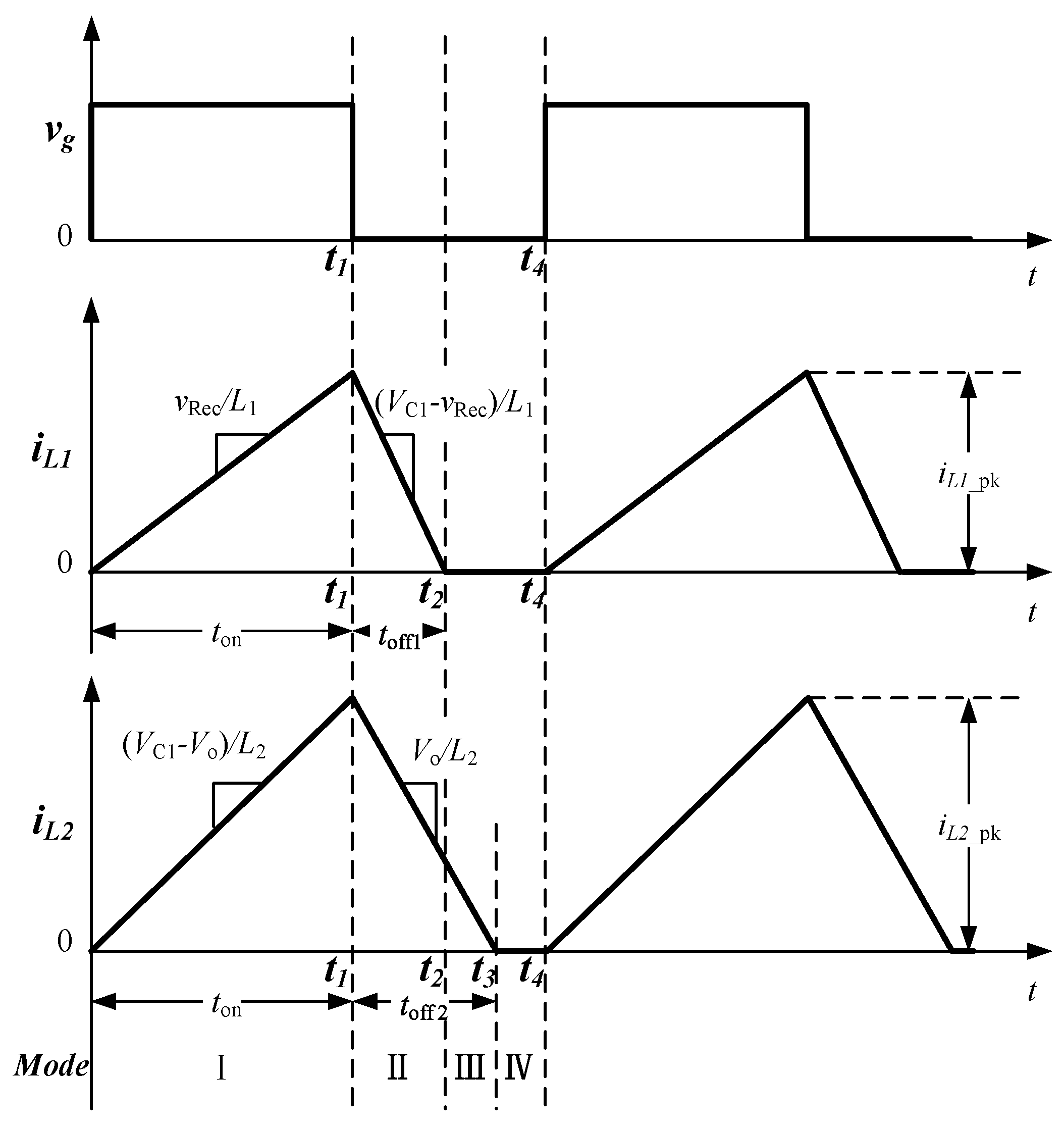
Cuk PFC can automatically realize PFC and simplifies the control circuit if both inductors operate in DCM with only a simple voltage mode control loop, so both output inductor L2 and input inductor L1 of the Cuk PFC converter operate in DCM in this paper. The waveforms of both inductor currents during two switching cycles are shown in Figure 2.
As can be seen from Figure 2, it is supposed that the input inductor current iL1 drops to 0 firstly. There are four operating modes of the Cuk PFC converter during one switching cycle.
Mode I: During this time period, the driving signal vg turns the switch S1 on; the input inductor L1 starts to be charged with energy by the rectified voltage vRec through diode D1 and switch S1. Meanwhile, the output inductor L2 is charged with energy by the voltage difference of the intermediate capacitor C1 and output capacitor Co. The rising slope of both inductor currents can be presented, respectively, as
d i L 1 d t = v Re c ( t ) L 1
d i L 2 d t = V C 1 V o L 2
where vRec(t) represents the rectified voltage; VC1 denotes the voltage of intermediate capacitor C1; Vo denotes output voltage.
Mode II: In this mode, the driving signal vg turns the switch S1 off, and the rectified voltage vRec and input inductor L1 start to release energy to the intermediate capacitor C1 through the diode D2. The output capacitor Co stores energy from the output inductor L2 through D2. The drop slope of both inductors can be given, respectively, as
d i L 1 d t = V C 1 v Re c ( t ) L 1
d i L 2 d t = V o L 2
Mode III: During this operating mode, the input inductor current iL1 drops to 0. The output capacitor Co still stores energy from the output inductor L2 through diode D2. The output inductor current iL2 continues to drop.
Mode IV: The switch S1 is still off, and diode D2 is in reverse bias during this operating mode. The output inductor current iL2 drops to 0, and the output capacitor Co provides power to the load.
According to Equation (1), the peak current iL1_pk(t) flowing through the input inductor L1 of the conventional Cuk PFC converter during one switching cycle can be expressed as
i L 1 _ pk ( t ) = V M | sin ( ω t ) | L 1 t on
where ton represents the conduction time of switch S1 during a switching period.
When the converter enters in steady-state operation, the discharge time toff1 of the input inductor can be obtained from the volt-second balance of the input inductor L1 as
t off 1 = V M | sin ( ω t ) | ( V C 1 V M | sin ( ω t ) | ) t on
Therefore, according to Equations (5) and (6), the rectified input current is equal to the average current iL1(t) through the input inductor during one switching cycle, and the rectified input current can be expressed as
| i in ( t ) | = i L 1 ( t ) = i L 1 _ pk ( t on + t off 1 ) 2 T s = V M t o n 2 | sin ( ω t ) | 2 T s L 1 [ 1 V M V C 1 | sin ( ω t ) | ]
where Ts is a switching cycle.
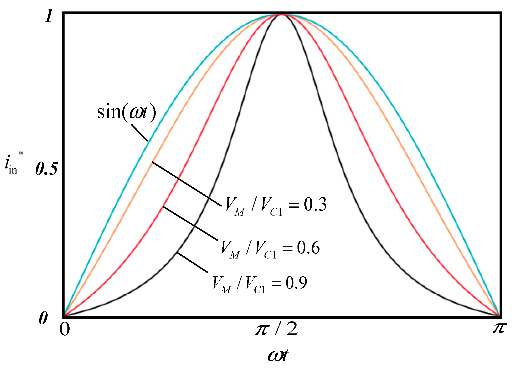
It is known from Equation (7) that there is a time component in the denominator of the converter input current iin(t), so the input current waveform of the conventional Cuk PFC converter will be distorted. For the sake of the convenience in analyzing the distortion of the input current waveform, the input current shown as Equation (7) is normalized with the base of VMton2/2TSL1(1 − VM/VC1), and the normalized input current i* waveform is illustrated in Figure 3. It can be found that the input current is related to the ratio of VM/VC1 for the conventional Cuk PFC converter. The larger the ratio of VM/VC1 is, the more serious the distortion of the input current is, and as the ratio of VM/VC1 gradually decreases, the input current distortion is reduced and gradually tends to be sinusoidal. In other words, the higher the voltage of the intermediate capacitor is, the closer the input current is to a sinewave.
According to Figure 2 and Equation (2), the peak current iL2_pk(t) of the output inductor L2 can be given as
i L 2 _ pk ( t ) = ( V C 1 V o ) L 2 t on
The output current and the average output inductor current are equal, so the output current Io is expressed as
I o = i L 2 ( t ) = i L 2 _ pk ( t on + t off 2 ) 2 T s
where toff2 is the discharge time of output inductor L2.
Because of the volt-second balance of inductor L2, toff2 is derived as
t off 2 = ( V C 1 V o ) V o t on
Substituting Equation (10) into (9), the output current Io can be rewritten as
I o = ( V C 1 V o ) V C 1 t on 2 2 T s L 2 V o
From Equation (11), ton can be derived as
t on = 2 T s L 2 V o I o ( V C 1 V o ) V C 1
By neglecting power loss, the input power should be equal to output power, so the input power can be given as
P in = 1 π 0 π i in ( t ) V M | sin ( ω t ) | d ( ω t ) = U o I o
According to (7) and (12), Equation (13) can be rewritten as
2 ( V C 1 V o ) M V M 2 2 π V C 1 0 π sin 2 ( ω t ) 1 V M V C 1 | sin ( ω t ) | d ( ω t ) = 1
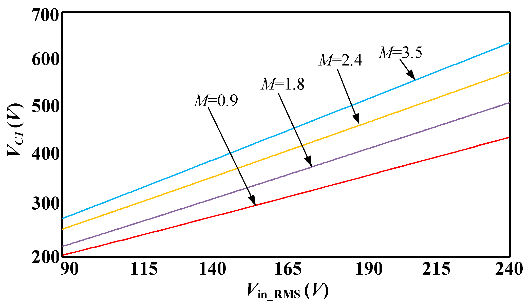
where M = L2/L1. According to the circuit parameters listed in Table 1, the relationship curves of the intermediate capacitor voltage VC1 and RMS input voltage Vin_RMS with different ratios M are shown in Figure 4. From Figure 4, it can be observed that the intermediate capacitor voltage VC1 increases as the Vin_RMS increases when M remains unchanged, and the intermediate capacitor voltage VC1 increases as the ratio M increases at a certain input voltage Vin_RMS.
According to (7) and (13), the PF of the conventional Cuk PFC converter can be derived as
P F = 2 P in V M I in _ RMS = 2 π 0 π sin 2 ( ω t ) 1 V M V C 1 | sin ( ω t ) | d ( ω t ) 0 π sin 2 ( ω t ) [ 1 V M V C 1 | sin ( ω t ) | ] 2 d ( ω t )
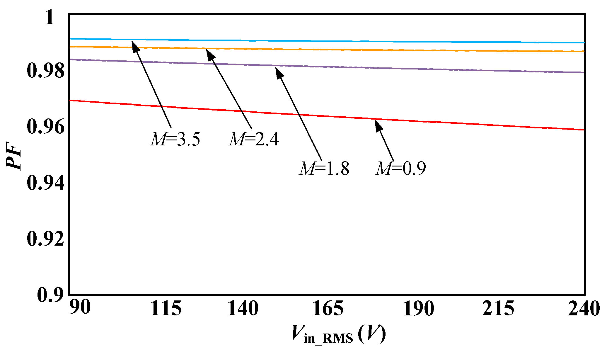
According to (14) and (15), the relation curves of the PF of the conventional Cuk PFC and RMS input voltage Vin_RMS with different ratios M are shown in Figure 5. Observing Figure 5, the PF decreases slightly as the Vin_RMS increases in the range from 90 V to 240 V when M is a constant value, and the PF decreases as the ratio M decreases when the converter input voltage Vin_RMS is a fixed value.
From the above analysis, for the conventional Cuk PFC converter, the intermediate capacitance voltage VC1 and PF are both related to the ratio M. The larger the ratio M is, the higher the PF is. Meanwhile, the intermediate capacitor voltage VC1 also increases, which will result in the need for higher breakdown voltage MOSFET and diode, so it is challenging to achieve high PF and low intermediate capacitor voltage at the same time.

3. Operation Principle and Performance Analysis of Cuk PFC Converter Based on Variable Inductor

3.1. Operation Principle

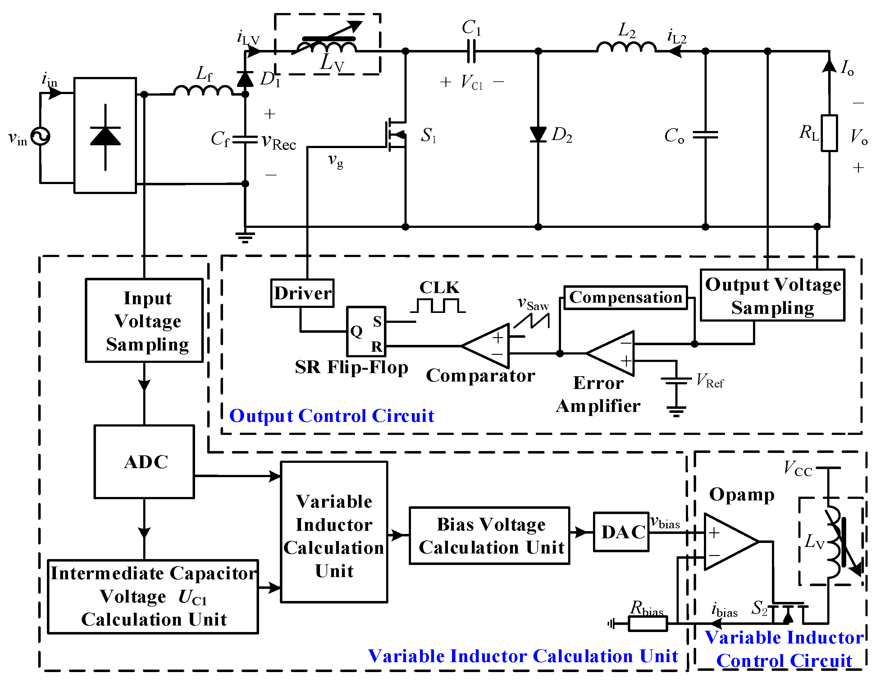
To reduce the intermediate capacitor voltage VC1 and increase the PF, a Cuk PFC converter with a variable inductor is proposed as shown in Figure 6. The proposed converter replaces the constant input inductor with the variable inductor and adds the calculation unit and control unit of variable inductor to realize the change of inductance. The main circuit of the proposed converter contains a rectifier bridge, filter inductor Lf, filter capacitor Cf, variable inductor LV, power switch S1, decoupling diode D1, intermediate capacitor C1, freewheeling diode D2, output capacitor Co, and output inductor L2.
The proposed Cuk PFC converter control circuit based on variable inductor mainly consists of output control circuit, variable inductor calculation unit, and variable inductor control circuit. The output control circuit uses voltage mode control; the variable inductor calculation unit is mainly composed of STM32; and the variable inductor control circuit is mainly composed of an opamp, bias resistor Rbias, and Mosfet S2. The operation principle of the control circuit is described as follows: the output error signal is obtained by amplifying the difference between the reference voltage VRef and feedback signal from the output voltage sampling circuit; the negative input of the comparator is connected to the error signal, and the positive input of the comparator is connected to the sawtooth wave signal vsaw; S1 is turned on at the start of the switching cycle, and S1 is turned off when vsaw reaches the error signal. Through sending the rectified input voltage, the sampling voltage, and the calculated intermediate capacitor voltage to the variable inductor calculation unit, the inductance of the variable inductor can be obtained. The bias voltage of the variable inductor control circuit is obtained by calculating the inductance of the variable inductor through bias voltage calculation unit. Through a voltage-controlled current source which is composed of an opamp, bias resistor Rbias, and Mosfet S2 which is operated at saturation region, the bias current ibias is obtained from the bias voltage vbias, and the required inductor is obtained by introducing the bias current into the auxiliary winding of the variable inductor through the variable inductor control circuit.
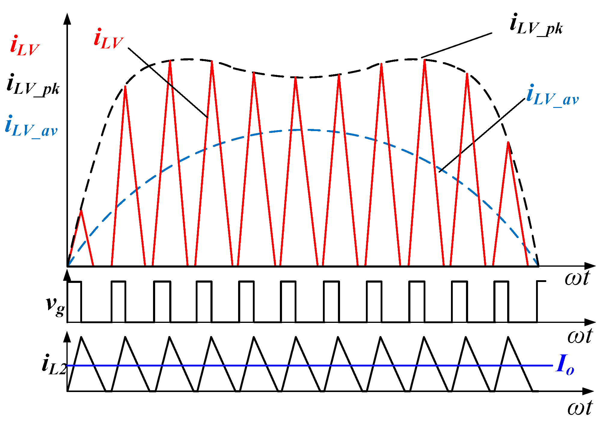
The proposed converter also operates in DCM. Key waveforms including the output inductor current iL2 and input inductor current iLV during half line cycle are shown in Figure 7.
With the same derivation method of input current in Section 2, the input current of the proposed converter can be obtained as
i in _ V I ( t ) = V M t on 2 sin ( ω t ) 2 T s L V [ 1 V M V C 1 | sin ( ω t ) | ]
According to Equation (16), if the variable inductor LV located in the denominator is variable with ωt during the half line cycle to make the denominator of Equation (16) become a constant value, then the purpose of correcting the input current can be achieved. LV is supposed to meet the formula as
L V [ 1 V M V C 1 | sin ( ω t ) | ] = L initial
where Linitial is a constant value. According to (17), the input current of (16) can be rewritten as
i in _ V I ( t ) = V M t on 2 sin ( ω t ) 2 T s L initial
Observing (18), the switch conduction time ton is unchanged when the Cuk PFC converter is at the stable operation state, so the input current is standard sinewave.
According to (15) and (18), the PF of the proposed converter can be obtained as
P F = 2 P in V M I in _ RMS = 2 t on 2 L initial V M 2 2 π T s 0 π sin 2 ( ω t ) d ( ω t ) t on 2 L initial V M 2 2 T s 1 π 0 π sin 2 ( ω t ) d ( ω t ) = 1
According to (19), unity PF can be achieved by the proposed converter.

3.2. Range of Inductor Variation

According to (18), the expression of the variable inductor LV can be rewritten as
L V = L initial [ 1 V M V C 1 | sin ( ω t ) | ]
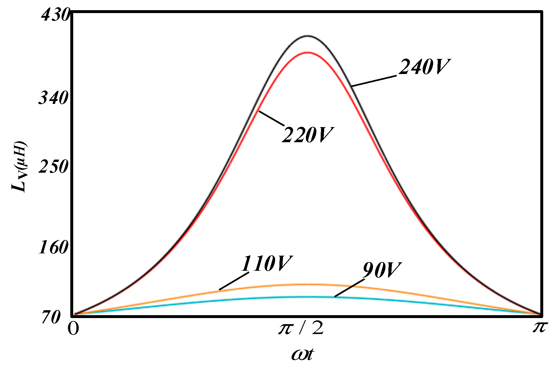
According to the circuit parameters listed in Table 1, the initial value of the variable inductor Linitial is 75 µH, and from Equation (20) and combined with the relation of the intermediate capacitor voltage VC1 and the input voltage Vin_RMS, the range of inductor variation can be plotted in a half line cycle as shown in Figure 8.
From Figure 8, it can be obtained that the variable inductor LV varies about 75 µH~410 µH when the converter input voltage Vin_RMS varies from 90 V to 240 V, and the variable inductor LV varies with the rectified input voltage during the half line cycle.

3.3. Operating Principle of Variable Inductor

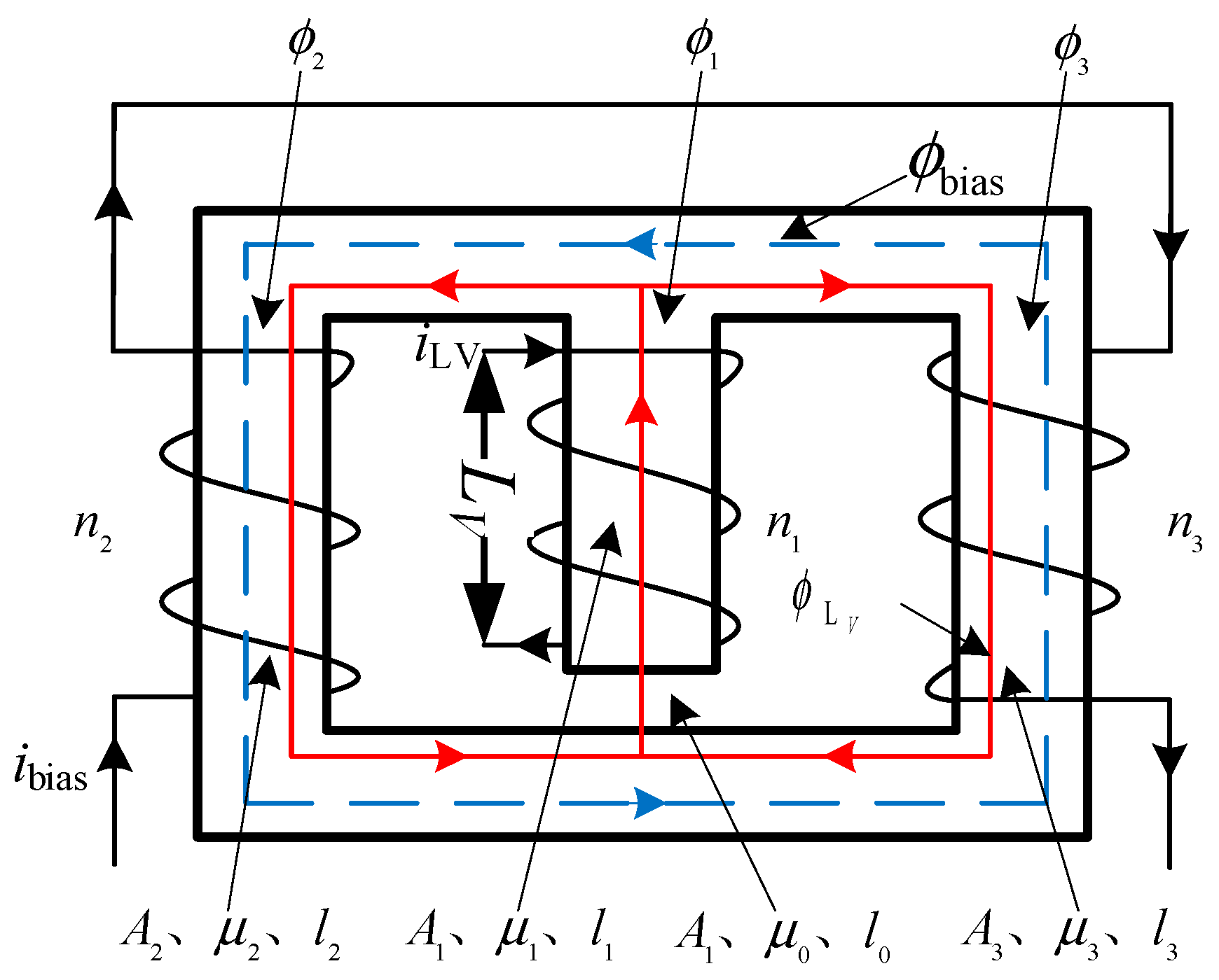
In this paper, the variable inductor LV uses an EI core as a magnetic core, and the basic model schematic of the variable inductor is shown in Figure 9. The middle leg is wound with n1 turns as the main winding of the input inductor of the proposed Cuk converter; the air gap l0 is opened to prevent the core from fast saturation; the auxiliary winding which is used to control the inductance is symmetrically wound on the side legs of the EI core; and the number of auxiliary winding turns on both side legs is the same as n2 and n3.
Because the air gap is opened in the middle leg, the permeability of the magnetic material is not the same, so the relative permeability of the middle winding is recorded as µ1, and the air permeability of the air gap is recorded as µ0. In order to reduce the induction potential on the auxiliary winding due to the change of current in the main winding, it is required that the number of auxiliary winding turns of the left and right legs is the same, and the relative permeability of the left leg is recorded as µ2 and is recorded as µ3 for the right leg.
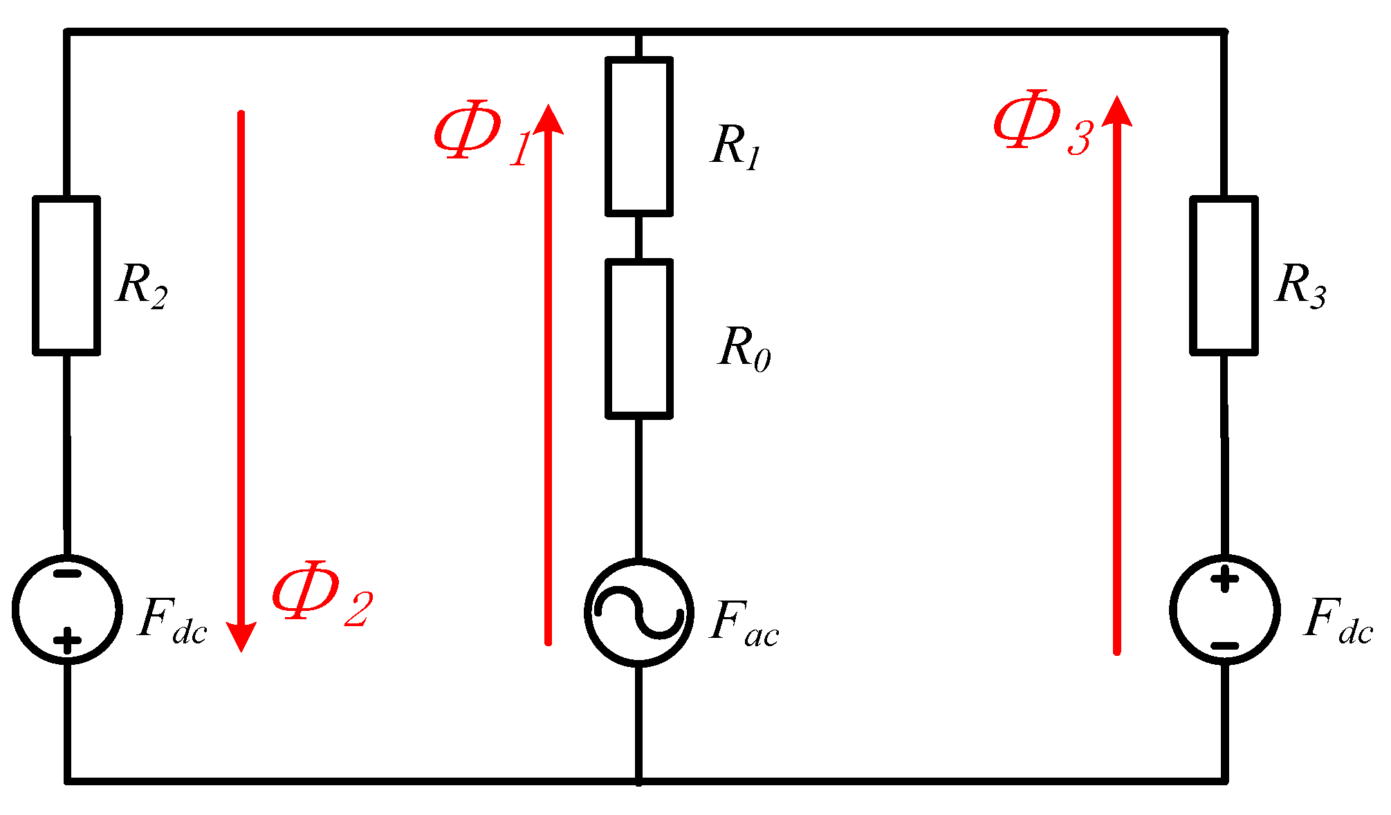
From Figure 9, it can be observed that the flux generated by the main winding flows from the middle leg through the left and right legs. When the main winding current iLV changes, the induced electromotive forces generated on the auxiliary windings in series with the left and right legs eliminate each other due to the opposite polarity, reducing the effect of the change in the main current on the inductor; when the bias current ibias changes, the flux generated by the auxiliary windings on both sides only flows in the side legs. Based on the above analysis, the equivalent reluctance model of the variable inductor using the EI core is illustrated in Figure 10.
As shown in Figure 10, Fac is the AC magnetomotive force; Fdc is the DC magnetomotive force generated by the bias current; Φ1, Φ2, and Φ3 are the fluxes of the middle, left, and right windings, respectively; R1, R2, and R3 are the reluctances of the middle, left, and right magnetic circuits; and R0 is the middle leg air gap reluctance, according to Ohm’s law of the magnetic circuit which can be expressed as
{ R 1 = l 1 μ 0 μ 1 A 1 R 2 = l 2 μ 0 μ 2 A 2 R 3 = l 3 μ 0 μ 3 A 3 R 0 = l 0 μ 0 A 0
where A1, A2, and A3 denote the section of the middle, left, and right legs, respectively; A0 is the section of the air gap; l1, l2, and l3 are the length of the middle leg, left leg, and right leg, respectively; l0 is the length of air gap.
Because of the characteristics of core structure and winding symmetry, it is derived that
{ A 1 = A 0 A 2 = A 3 l 2 = l 3 n 2 = n 3
From the definition of the magnetomotive force and its relationship with the reluctance, the relation of magnetic field intensity and reluctance is deduced as
F = H l = Φ R
According to Figure 10 and Equation (23), combined with the Kirchhoff’s law of the magnetic circuit, it is obtained that
{ H 1 l 1 + H 0 l 0 H 3 l 3 = n 1 i 1 n 3 i 3 H 1 l 1 + H 0 l 0 + H 2 l 2 = n 1 i 1 + n 2 i 2 Φ 2 = Φ 3 + Φ 1
where H1, H2, H3, and H0 are the magnetic field strengths of the middle, left, right, and airgap legs. Substituting (23) into (24), it is derived as
{ Φ 1 ( R 1 + R 0 ) Φ 3 R 3 = n 1 i 1 n 3 i 3 Φ 1 ( R 1 + R 0 ) + Φ 2 R 2 = n 1 i 1 + n 2 i 2 Φ 2 = Φ 3 + Φ 1
By simplifying (25), the expression for the main flux of the intermediate winding or variable inductor can be obtained as
Φ 1 = ( R 3 R 2 ) n 2 i 2 + ( R 3 + R 2 ) n 1 i 1 R 2 R 3 + R 2 ( R 1 + R 0 ) + R 3 ( R 1 + R 0 )
Substituting (21) into (26), the relationship between the main flux and the permeability of each segment and length can be deduced as
Φ 1 = 1 [ l 2 μ 0 ( μ 2 + μ 3 ) A 2 n 1 i 1 + l 1 μ 0 μ 1 A 1 n 1 i 1 + l 0 μ 0 A 1 n 1 i 1 ] + 1 [ l 2 μ 0 ( μ 2 μ 3 ) A 2 n 2 i 2 + l 1 μ 0 μ 1 A 1 ( μ 2 μ 3 μ 2 + μ 3 ) n 2 i 2 + l 0 μ 0 A 1 ( μ 2 μ 3 μ 2 + μ 3 ) n 2 i 2 ]
Combining the relationship between inductor and magnetic flux, the expression for variable inductor is derived as
L V = n 1 Φ 1 i 1 = 1 ( l 2 2 μ 0 μ var A 2 n 1 2 + l 1 μ 0 μ 1 A 1 n 1 2 + l 0 μ 0 A 1 n 1 2 )
where µvar is equal to the relative permeability of left and right legs, and it can be changed according to the value of the injected DC bias current ibias, which presents a negative correlation trend of the variable inductance and the bias current ibias. As the bias current ibias increases, µvar gradually decreases, resulting in a decrease in the inductance of the variable inductor until the bias current reaches ibias_max, which completely saturates the left and right legs, and the variable inductor decreases to minimum value.

3.4. The Voltage of Intermediate Capacitor

Because of power conservation, substitution of (16) into (13), the relationship between the input voltage and the voltage of the intermediate capacitor of the proposed converter is given as
L 2 L initial 2 ( V C 1 V o ) V M 2 2 π V C 1 0 π sin 2 ( ω t ) d ( ω t ) = 1
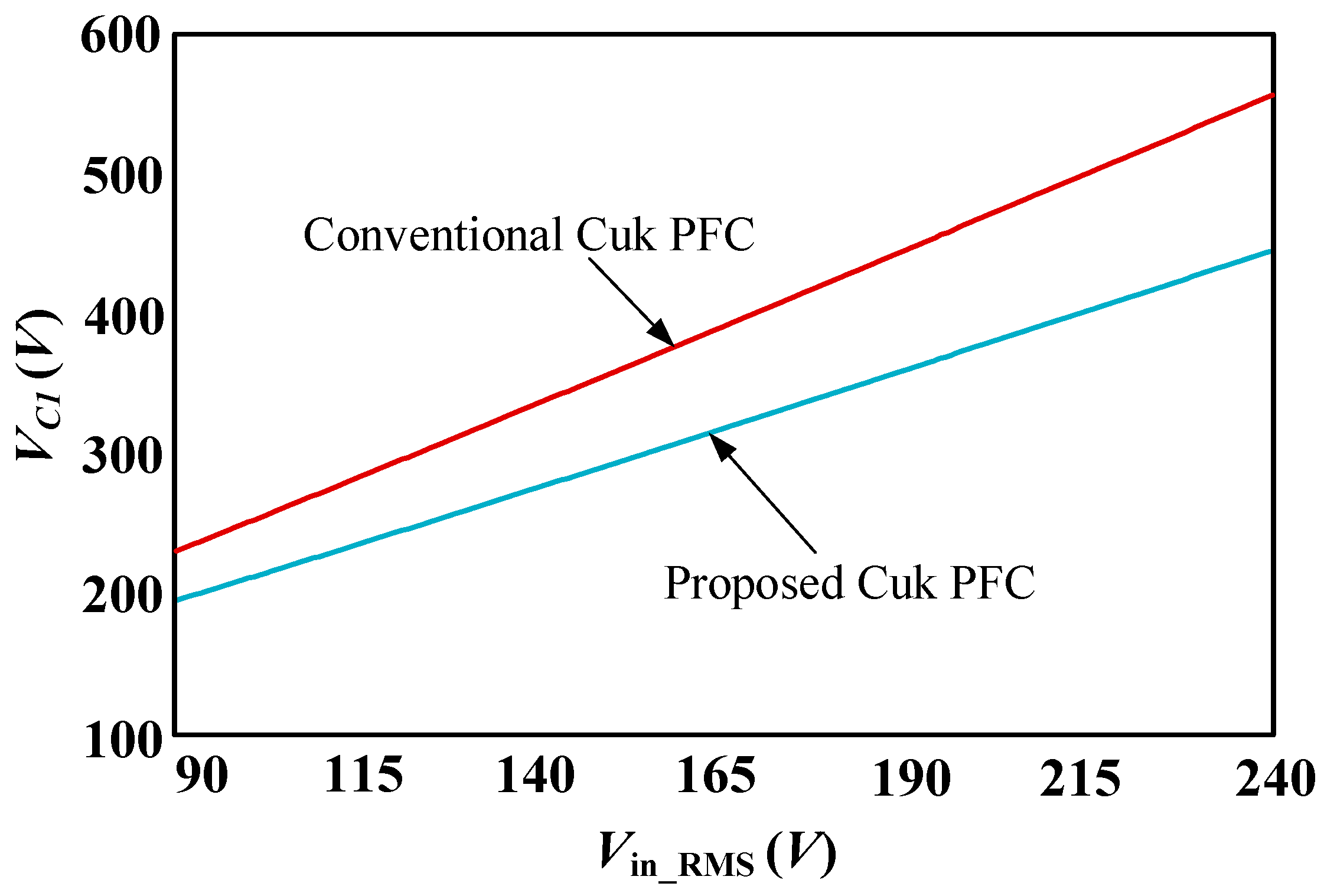
The variation of the intermediate capacitor voltage VC1 with input voltage Vin_RMS can be calculated and plotted, as shown in the blue curve in Figure 11. To facilitate comparison with the intermediate capacitance voltage of the traditional Cuk PFC converter, the input inductor and output inductor are chosen in Table 1, and the red curve shown in Figure 11 is the conventional Cuk PFC when M = L2 /L1 = 2.4.
From Figure 11, it is obvious that the proposed converter has a significant reduction in the intermediate capacitor voltage VC1 during the variation of input voltage Vin_RMS from 90 V to 240 V compared with the traditional Cuk PFC converter.

3.5. Peak Current of Input Inductor

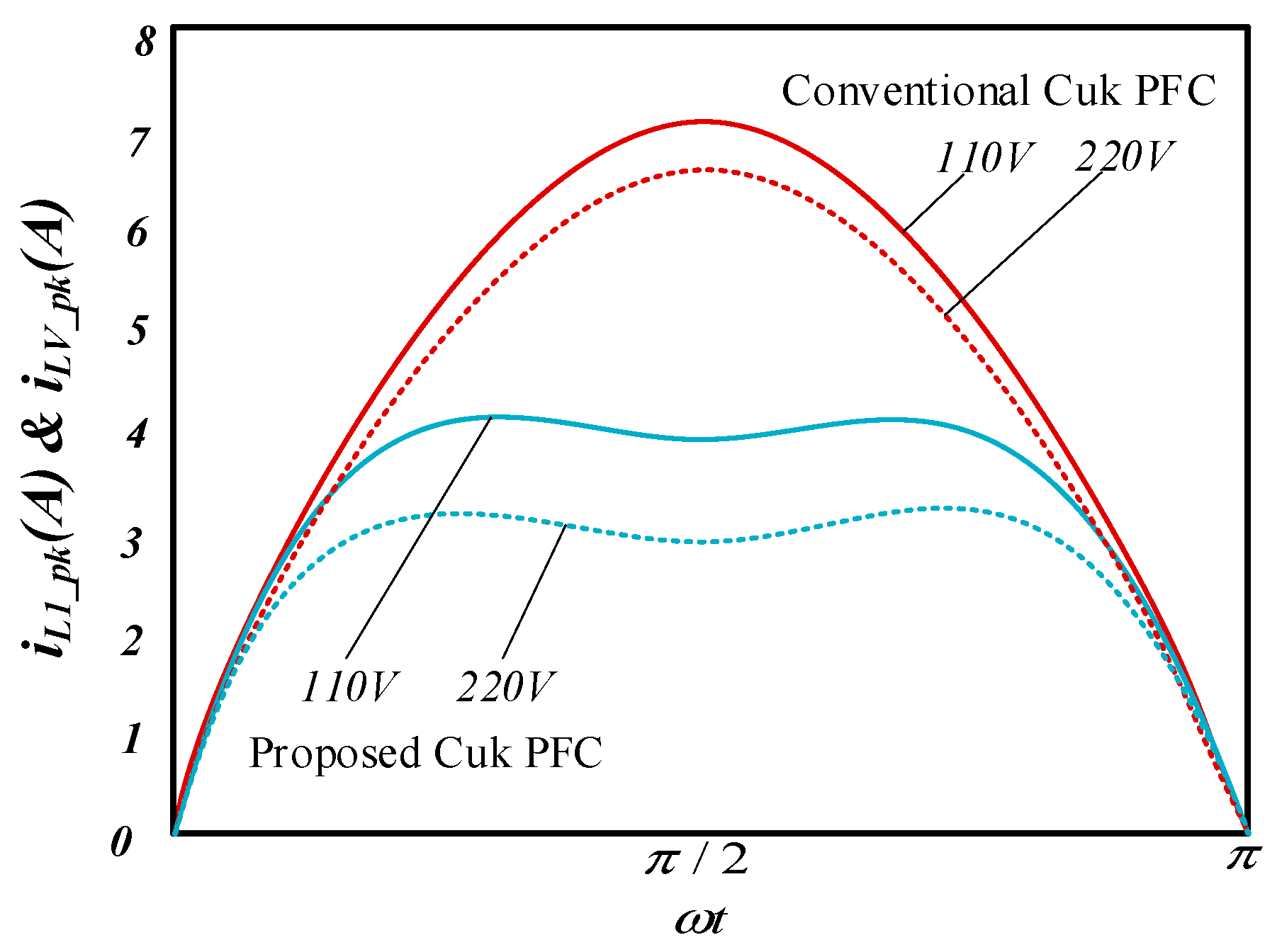
Substituting Equation (20) into (5), the envelope curves of the peak current of the input inductor comparison of both the traditional and proposed converters can be plotted for a half line cycle, as depicted in Figure 12.
From Figure 12, the peak current of the input inductor of the proposed Cuk PFC converter is significantly reduced, which will help to diminish the current stress of the switch.

3.6. Conditions of Both Input and Output Inductors Operating in DCM

In order to make the output inductor current iL2 operate in DCM, it should be ensured that the sum of the on-time ton and the off-time toff2 of the output inductor is less than one switching cycle Ts.
t on + t off 2 < T s
Substituting Equations (10) and (12) into the above equation, the output inductor current iL2 operating in DCM can be obtained as
L 2 ( V C 1 V o ) U o T s 2 V C 1 I o
According to (31) and combined with the analysis of the intermediate capacitor voltage VC1, the critical inductor value of the output inductor L2 operating in DCM when the input voltage Vin_RMS is 90 V~240 V can be obtained as shown in Figure 13.
According to (13) and (18), the relationship of ton and output power with variable inductor can be obtained as
t on 2 L initial V M 2 2 π T s 0 π sin 2 ( ω t ) d ( ω t ) = P o
The relationship between the initial inductance of variable inductor and the on-time ton is derived as
t on = 4 T s L initial P o V M 2
Within the half line period, the higher the transient rectified input voltage is, the larger the input inductor current peak is, and the longer the inductor current iLV discharge time within the half line cycle is. When |sin(ωt)| = 1 at the input voltage peak VM, the iLV discharge time reaches the maximum, and the maximum discharge time can be derived as
t off 1 _ max = V M ( V C 1 V M ) t on
The limit of the input inductor current iLV in DCM can be obtained as
t on + t off 1 _ max < T s
Substituting Equations (33) and (34) into (35) and simplifying the above equation, the limit of the initial inductance of variable inductor can be deduced as
L initial ( V C 1 V M ) 2 V M 2 T s 4 P o V C 1 2
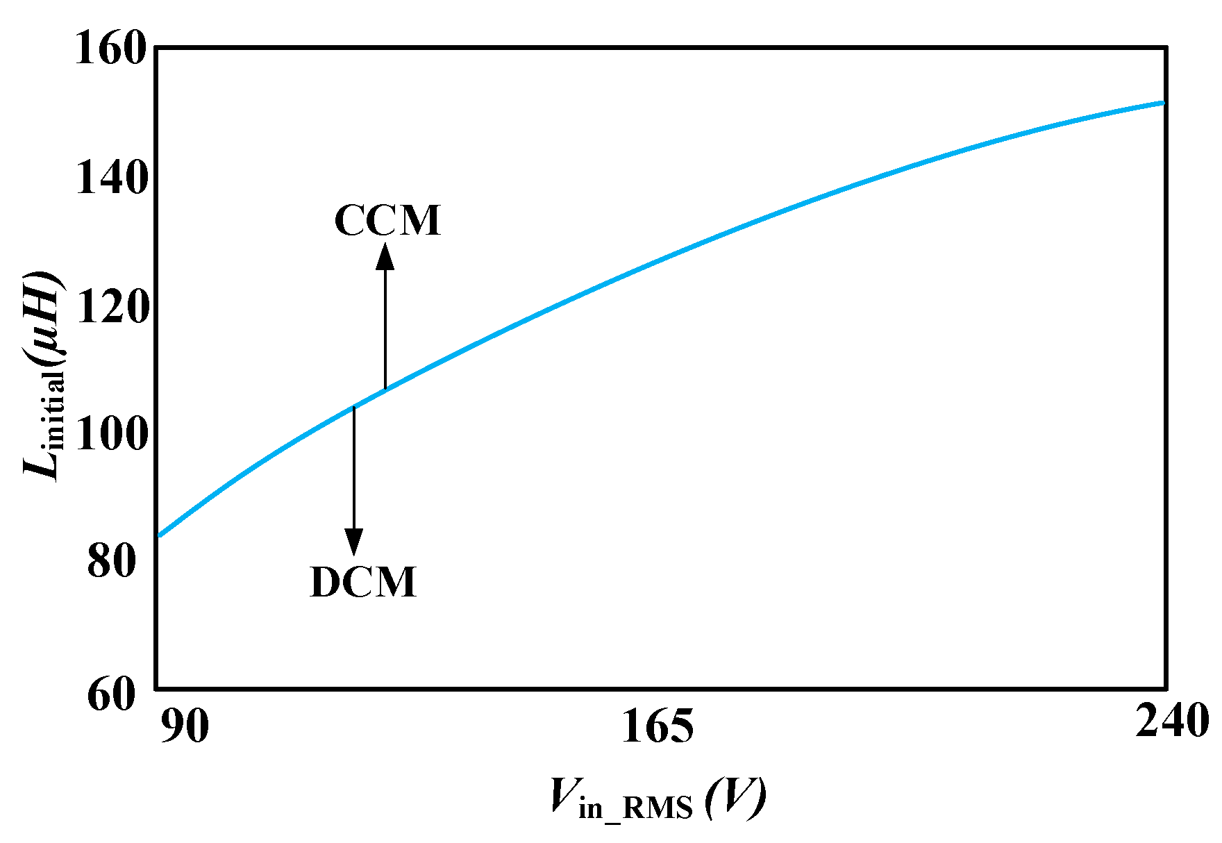
From (36) and combined with the circuit parameters, it is obtained that the initial inductance of variable inductor variation range is about 84 µH~152 µH at the input voltage Vin_RMS of 90 V~240 V, and its variation curve is shown in Figure 14.
To ensure that both input and output inductors operate in DCM over the input voltage variation range, 75 µH is selected as the initial inductance of the variable inductor to meet the critical value at 90 Vac, and 180 µH is chosen as the output inductor to meet the DCM of the output inductor of the proposed Cuk PFC converter.

4. Experimental Results

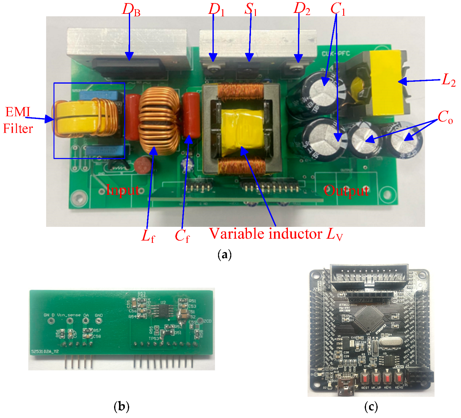
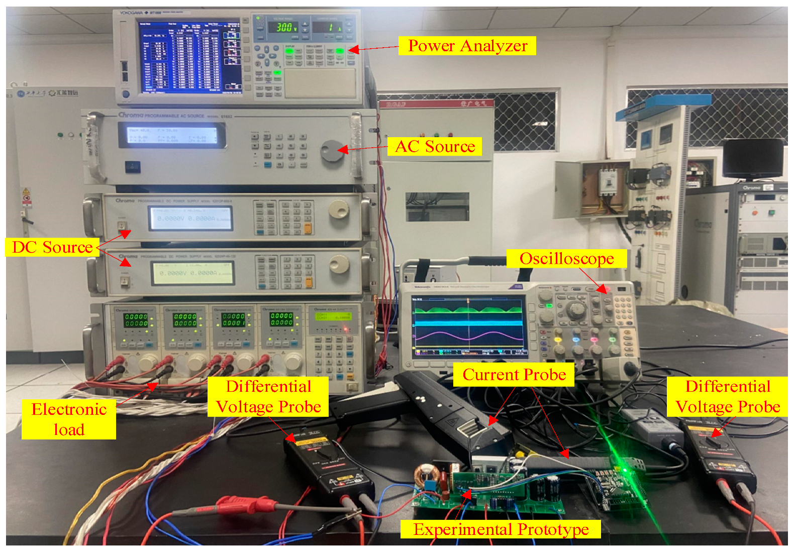
For the purpose of checking the correctness of the theoretical analysis, a 108 W experimental prototype has been built in the laboratory to compare the experimental results of both the traditional and proposed Cuk PFC converters. The specifications and the circuit parameters are listed in Table 1. The pictures of the experimental prototype and the experimental platform are presented in Figure 15 and Figure 16, respectively.
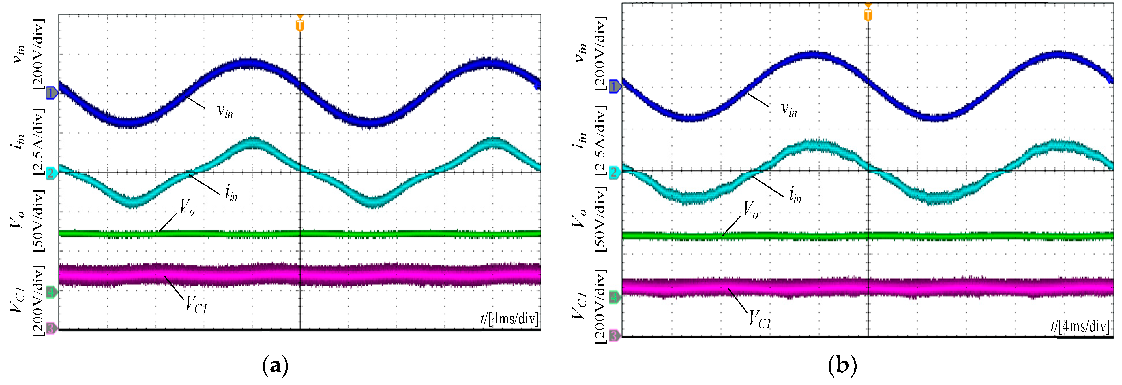
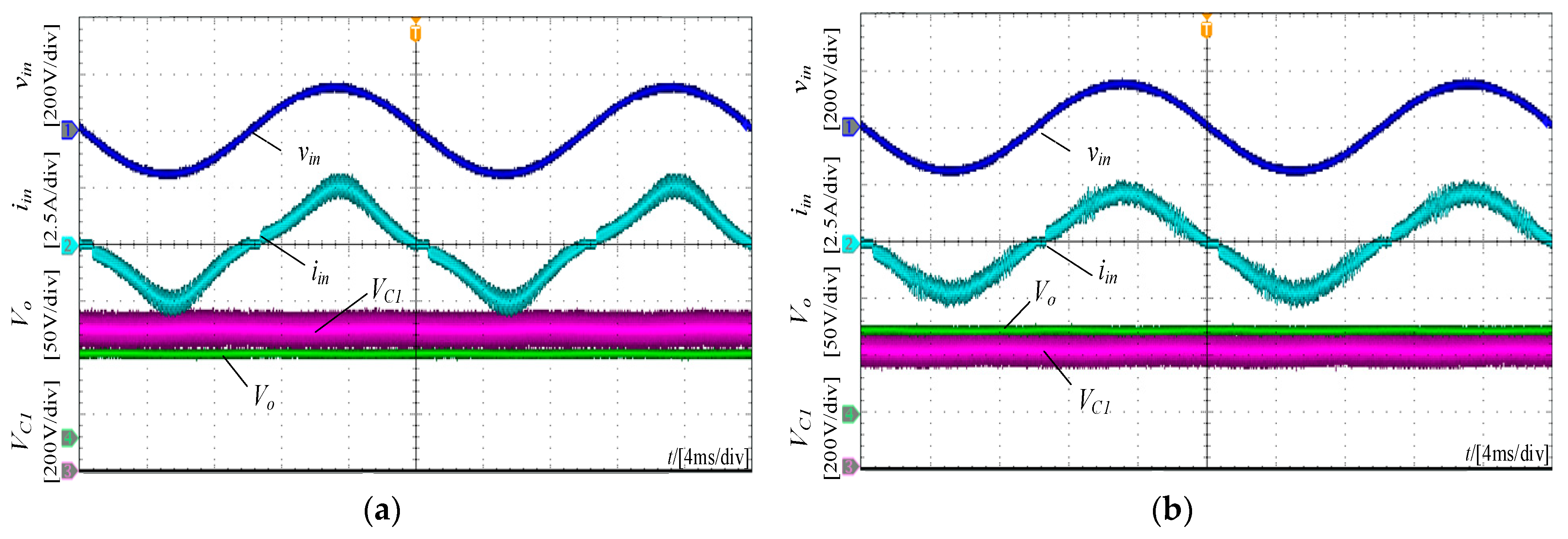
The experimental results of input current iin, input voltage vin, output voltage Vo, and intermediate capacitor voltage VC1 for the traditional Cuk PFC converter and the proposed Cuk PFC converter with variable inductor when the input voltage is 110 Vac and 220 Vac are illustrated, respectively, in Figure 17 and Figure 18. According to Figure 17a and Figure 18a, it can be observed that the conventional Cuk PFC converter can obtain a stable output voltage at 72 V. Harmonic distortion occurs in the input current, and the voltage of the intermediate capacitor reaches 280 V and 520 V when the input voltage is 110 Vac and 220 Vac, respectively. According to Figure 17b and Figure 18b, it can be noticed that the proposed Cuk PFC converter can obtain a stable output voltage at 72 V without obvious twice line frequency output voltage ripple; the waveform of input current is corrected to sine-wave with variable inductor; and the intermediate capacitor voltage is reduced to 240 V and 410 V when the input voltage is 110 Vac and 220 Vac, respectively. Therefore, compared with the conventional Cuk PFC converter, the input current of the proposed Cuk PFC converter based on variable inductor can obtain near-ideal sine-wave input current, and the intermediate capacitor voltage of the proposed converter is significantly reduced.
The inductor current waveforms experimental results of both converters at 110 Vac are illustrated in Figure 19, which shows that the peak input inductor current decreases from 8 A for the conventional Cuk PFC converter to 6 A for the proposed Cuk PFC converter. It also can be obtained that the peak input inductor current decreases from 7.5 A to 5.3 A by variable inductor control at 220 Vac in Figure 20.
The variable inductor current iLV is slightly distorted as illustrated in Figure 19d and Figure 20d, which is due to the small bias current applied to the auxiliary winding, and the inductance of the variable inductor is more easily affected by the main winding current. The operating point of the variable inductor is shifted towards the saturation region [35,36]. It also causes the actual inductance of the variable inductor to not reach the theoretical calculation value, which leads to a higher actual inductor current than the theoretically derived value.
The comparison data of the input current harmonic content test results of both the traditional and proposed converters are presented in Figure 21. The experimental data of PF, efficiency, and THD are illustrated in Figure 22. From Figure 21 and Figure 22c, compared with the traditional Cuk PFC converter, the proposed converter is easier to meet the requirement of IEC61000-3-2 class D. The THD and third harmonic current are significantly reduced by using the variable inductor. From Figure 22a, the PF of the proposed converter with variable inductor is enhanced over the input voltage variation range. Due to the application of the variable inductor, the PF is increased from 0.982 to 0.995 at 110 Vac, and the PF is enhanced from 0.975 to 0.981 at 220 Vac. Because of the influence of the variable inductor main current on the inductor saturation level, the actual inductor value does not reach the theoretical calculated value, which makes the PF of experimental test results with variable inductor lower than the theoretical analysis result. From Figure 22b, the efficiency is improved obviously by using the variable inductor, and the efficiency can be higher than 90% at 90 Vac input voltage.

5. Conclusions

A Cuk PFC converter based on variable inductor is proposed in this paper, which uses real-time variations of inductor to solve the problem of the traditional Cuk PFC converter including low power factor and high intermediate capacitor voltage. The operation principles of the proposed converter are analyzed in detail, and the analyses of PF, the voltage of intermediate capacitor, and design considerations are provided. For the purpose of verifying the feasibility of the proposed scheme, an experimental prototype of 108W was built and tested. The experimental test results indicated that the proposed Cuk PFC converter based on variable inductor can significantly enhance the PF, decrease the intermediate capacitor voltage, and increase efficiency.

Author Contributions

Conceptualization, T.Y. and T.C. (Tong Chen); methodology, T.Y., T.C. (Tong Chen) and A.H.; formal analysis, T.Y., T.C. (Tong Chen), A.H. and W.C.; validation, T.Y., T.C. (Tong Chen), A.H., W.C. and T.C. (Taiqiang Cao); investigation, T.Y., T.C. (Tong Chen) and T.C. (Taiqiang Cao); writing—original draft preparation, T.Y., T.C. (Tong Chen) and A.H.; writing—review and editing, T.Y., T.C. (Tong Chen), A.H., W.C. and T.C. (Taiqiang Cao). All authors have read and agreed to the published version of the manuscript.

Funding

This work was supported by the National Natural Science Foundation of China under Grant No. 51977178 and Chunhui Project Foundation of Education Department of China under Grant Z2017081, Key Laboratory of Fluid and Power Machinery (Xihua University) of Ministry of Education (No. SZJJ2016-012).

Data Availability Statement

Not applicable.

Conflicts of Interest

The authors declare no conflict of interest.

References

  1. Qi, W.; Li, S.; Tan, S.; Hui, S. Design considerations for voltage sensorless control of a PFC single-phase rectifier without electrolytic capacitors. IEEE Trans. Ind. Electron. 2020, 67, 1878–1889. [Google Scholar] [CrossRef]
  2. Yao, K.; Li, J.; Shao, F.; Zhang, B. Parallel fixed switching frequency CRM and DCM Boost PFC converter with high power factor. IEEE Trans. Power Electron. 2022, 37, 3247–3258. [Google Scholar] [CrossRef]
  3. Baek, J.; Kim, J.; Lee, J.; Park, M.; Moon, G. A new standby structure integrated with Boost PFC converter for server power supply. IEEE Trans. Power Electron. 2019, 34, 5283–5293. [Google Scholar] [CrossRef]
  4. Luo, H.; Xu, J.; Luo, Y.; Sha, J. A digital pulse train controlled high power factor DCM Boost PFC converter over a universal input voltage range. IEEE Trans. Ind. Electron. 2019, 66, 2814–2824. [Google Scholar] [CrossRef]
  5. Cui, Y.; Han, H.; Liu, Y.; Xu, G.; Su, M.; Xie, S. An efficiency-improved single-phase PFC rectifier with active power decoupling. IEEE Trans. Power Electron. 2022, 37, 10784–10796. [Google Scholar] [CrossRef]
  6. Chen, Z.; Xu, J.; Liu, X.; Davari, P.; Wang, H. High power factor bridgeless integrated Buck-type PFC converter with wide output voltage range. IEEE Trans. Power Electron. 2022, 37, 12577–12590. [Google Scholar] [CrossRef]
  7. Liu, X.; Wan, Y.; He, M.; Zhou, Q.; Meng, X. Buck-type single-switch integrated PFC converter with low total harmonic distortion. IEEE Trans. Ind. Electron. 2021, 68, 6859–6870. [Google Scholar] [CrossRef]
  8. Liu, X.; Li, X.; Zhou, Q.; Xu, J. Single-inductor dual-output Buck–Boost power factor correction converter. IEEE Trans. Power Electron. 2015, 62, 943–952. [Google Scholar] [CrossRef]
  9. Bang, T.; Park, J. Development of a ZVT-PWM Buck cascaded Buck–Boost PFC converter of 2 kW with the widest range of input voltage. IEEE Trans. Ind. Electron. 2018, 65, 2090–2099. [Google Scholar] [CrossRef]
  10. Brkovic, M.; Cuk, S. Automatic current shaper with fast output regulation and soft-switching. In Proceedings of the Intelec 93: 15th International Telecommunications Energy Conference, Paris, France, 27–30 September 1993; pp. 379–386. [Google Scholar]
  11. Bodetto, M.; Aroudi, A.; Cid-Pastor, A.; Calvente, J.; Martínez, L. Design of AC–DC PFC high-order converters with regulated output current for low-power applications. IEEE Trans. Power Electron. 2016, 31, 2012–2025. [Google Scholar] [CrossRef]
  12. Ananthapadmanabha, B.; Maurya, R.; Arya, S. Improved power quality switched inductor Cuk converter for battery charging applications. IEEE Trans. Power Electron. 2018, 33, 9412–9423. [Google Scholar] [CrossRef]
  13. Soares, G.; Almeida, P.; Pinto, D.; Braga, H. A single-stage high efficiency long-life off-line LED driver based on the DCM Cuk converter. In Proceedings of the IECON 2012—38th Annual Conference on IEEE Industrial Electronics Society, Montreal, QC, Canada, 25–28 October 2012; pp. 4509–4514. [Google Scholar]
  14. Pathare, P.; Panchade, V. Power quality improvement of BLDC motor drive using Cuk PFC converter. In Proceedings of the 2020 IEEE International Conference on Computing, Power and Communication Technologies (GUCON), Greater Noida, India, 2–4 October 2020; pp. 177–181. [Google Scholar]
  15. Pandey, R.; Singh, B. A Power-Factor-Corrected LLC resonant converter for electric vehicle charger using Cuk converter. IEEE Trans. Ind. Appl. 2019, 55, 6278–6286. [Google Scholar] [CrossRef]
  16. Liu, Y.; Zhang, H.; Wang, H.; Dan, H.; Su, M.; Pan, X. Peak and valley current control for Cuk PFC converter to reduce capacitance. IEEE Trans. Power Electron. 2022, 37, 313–321. [Google Scholar] [CrossRef]
  17. Yang, H.; Chiang, W.; Chen, C. Implementation of bridgeless Cuk power factor corrector with positive output voltage. IEEE Trans. Ind. Appl. 2015, 51, 3325–3333. [Google Scholar] [CrossRef]
  18. Lin, X.; Jin, Z.; Wang, F.; Luo, J. A novel bridgeless Cuk PFC converter with further reduced conduction losses and simple circuit structure. IEEE Trans. Ind. Electron. 2021, 68, 10699–10708. [Google Scholar] [CrossRef]
  19. Dutta, S.; Gangavarapu, S.; Rathore, A.; Singh, R.; Mishra, S.; Khadkikar, V. Novel single-phase Cuk-derived bridgeless PFC converter for on-board EV charger with reduced number of components. IEEE Trans. Ind. Appl. 2022, 58, 3999–4010. [Google Scholar] [CrossRef]
  20. Perdigo, M.; Alonso, J.; Dalla Costa, M. Using magnetic regulators for the optimization of universal ballasts. IEEE Trans. Power Electron. 2008, 23, 3126–3134. [Google Scholar] [CrossRef]
  21. Alonso, J.; Perdigao, M.; Dalla Costa, M.; Zhang, S.; Wang, Y. Analysis and experimentation of the quad-U variable inductor for power electronics applications. IET Power Electron. 2018, 11, 2330–2337. [Google Scholar] [CrossRef]
  22. Perdigao, M.; Menke, M.; Seidel, A.; Pinto, R.; Alonso, J. A review on variable inductors and variable transformers: Applications to lighting drivers. IEEE Trans. Ind. Appl. 2016, 52, 531–547. [Google Scholar] [CrossRef]
  23. Medini, D.; Yaakov, S. A current-controlled variable-inductor for high frequency resonant power circuits. In Proceedings of the IEEE Applied Power Electronics Conference and Exposition, Orlando, FL, USA, 13–17 February 1994; pp. 219–225. [Google Scholar]
  24. Alonso, J.; Perdigao, M.; Abdelmessih, G.; Dalla Costa, M.; Wang, Y. SPICE modeling of variable inductors and its application to single inductor LED driver design. IEEE Trans. Ind. Appl. 2017, 64, 5894–5903. [Google Scholar] [CrossRef]
  25. Alonso, J.; Martinez, G.; Perdigao, M. A systematic approach to modeling complex magnetic devices using SPICE: Application to Variable Inductors. IEEE Trans. Power Electron. 2016, 31, 7735–7746. [Google Scholar] [CrossRef]
  26. Alonso, J.; Martinez, G.; Perdigao, M. Modeling magnetic devices using SPICE: Application to variable inductors. In Proceedings of the 2016 IEEE Applied Power Electronics Conference and Exposition (APEC), Long Beach, CA, USA, 20–24 March 2016; pp. 1115–1122. [Google Scholar]
  27. Saeed, S.; Garcia, J.; Perdigao, M.; Costa, V.; Baptista, B.; Mendes, A. Improved inductance calculation in variable power inductors by adjustment of the reluctance model through magnetic path analysis. IEEE Trans. Ind. Appl. 2021, 57, 1572–1587. [Google Scholar] [CrossRef]
  28. Perdigao, M.; Trovao, J.; Alonso, J.; Saraiva, E. Large-signal characterization of power inductors in EV bidirectional DC–DC converters focused on core size optimization. IEEE Trans. Ind. Electron. 2015, 62, 3042–3051. [Google Scholar] [CrossRef]
  29. Beraki, M.; Trovao, J.; Perdigao, M.; Dubois, M. Variable inductor based bidirectional DC–DC converter for electric vehicles. IEEE Trans. Veh. Technol. 2017, 66, 8764–8772. [Google Scholar] [CrossRef]
  30. Zhu, X. High-efficiency WPT system for CC/CV charging based on double-half-bridge inverter topology with variable inductors. IEEE Trans. Power Electron. 2022, 37, 2437–2448. [Google Scholar] [CrossRef]
  31. Martins, M.; Perdigao, M.; Mendes, M.; Pinto, R.; Alonso, J. Analysis, Design, and Experimentation of a dimmable resonant-switched-capacitor LED driver with variable inductor control. IEEE Trans. Power Electron. 2017, 32, 3051–3062. [Google Scholar] [CrossRef]
  32. Alonso, J.; Costa, M.; Rico-Secades, M. Investigation of a new control strategy for electronic ballasts based on variable inductor. IEEE Trans. Ind. Electron. 2008, 55, 3–10. [Google Scholar] [CrossRef]
  33. Wei, Y.; Luo, Q.; Woldegiorgis, D. Analysis of a magnetically controlled single stage LLC resonant converter. In Proceedings of the 2020 IEEE Applied Power Electronics Conference and Exposition (APEC), Orleans, LA, USA, 15–19 March 2020; pp. 1257–1263. [Google Scholar]
  34. Wei, Y.; Luo, Q.; Alonso, J. A magnetically controlled single-stage AC–DC converter. IEEE Trans. Power Electron. 2020, 35, 8872–8877. [Google Scholar] [CrossRef]
  35. Zhang, Z.; Yao, K.; Ma, C. All-fixed switching frequency control of CRM Boost PFC converter based on variable inductor in a wide input voltage range. In Proceedings of the 2019 IEEE Energy Conversion Congress and Exposition (ECCE), Baltimore, MD, USA, 29 September–3 October 2019; pp. 1434–1441. [Google Scholar]
  36. Yao, K.; Zhang, Z.; Yang, J. Quasi-fixed switching frequency control of CRM Boost PFC converter based on variable inductor in wide input voltage range. IEEE Trans. Power Electron. 2020, 36, 1814–1827. [Google Scholar] [CrossRef]
  37. Yao, Y.; Liu, J.; Zhu, D.; Jin, Z. High power factor CRM Boost PFC converter with optimum switching frequency variation range control based on variable inductor. IEEE Trans. Power Electron. 2021, 36, 11019–11025. [Google Scholar] [CrossRef]
  38. Hidalgo, H.; Vázquez, N.; Orosco, R.; Huerta-Ávila, H.; Pinto, S.; Estrada, L. Floating interleaved Boost converter with zero-ripple input current using variable inductor. Technologies 2023, 11, 21. [Google Scholar] [CrossRef]
  39. Choi, S.; Shin, J.; Imaoka, J.; Yamamoto, M. Voltage-controlled variable inductor for fixed-frequency critical conduction mode operation. IEEE Trans. Ind. Electron. 2023, 70, 5707–5716. [Google Scholar] [CrossRef]
Figure 1. Main circuit diagram of the conventional Cuk PFC converter.
Electronics 12 02245 g001
Figure 2. Key operation waveforms.
Electronics 12 02245 g002
Figure 3. Normalized input current waveform of the conventional Cuk PFC converter.
Electronics 12 02245 g003
Figure 4. The relation curves of RMS input voltage Vin_RMS and the voltage VC1 across the intermediate capacitor with different ratios M.
Electronics 12 02245 g004
Figure 5. The relationship curve of PF and RMS input voltage Vin_RMS with different ratios M.
Electronics 12 02245 g005
Figure 6. Block diagram of the Cuk PFC converter based on variable inductor.
Electronics 12 02245 g006
Figure 7. Key waveforms of the Cuk PFC converter based on variable inductor.
Electronics 12 02245 g007
Figure 8. The variation range of input inductor LV.
Electronics 12 02245 g008
Figure 9. The basic model schematic of the variable inductor LV with EI core.
Electronics 12 02245 g009
Figure 10. Equivalent reluctance model of variable inductor using EI core.
Electronics 12 02245 g010
Figure 11. The relationship of intermediate capacitor voltage and input voltage.
Electronics 12 02245 g011
Figure 12. Envelope curves of the input inductor peak currents iL1_pk and iLV_pk.
Electronics 12 02245 g012
Figure 13. The critical inductor of the output inductor L2 operating in DCM.
Electronics 12 02245 g013
Figure 14. The critical initial value of the variable inductor operating in DCM.
Electronics 12 02245 g014
Figure 15. Experimental Prototype. (a) Main circuit; (b) Output control circuit; (c)Variable inductor calculation circuit.
Electronics 12 02245 g015
Figure 16. Experimental Platform.
Electronics 12 02245 g016
Figure 17. Experimental waveform of vin, iin, Vo, and VC1 at 110 V input. (a) Conventional Cuk PFC converter; (b) Proposed Cuk PFC converter.
Electronics 12 02245 g017
Figure 18. Experimental waveform of vin, iin, Vo, and VC1 at 220 V input. (a) Conventional Cuk PFC converter; (b) Proposed Cuk PFC converter.
Electronics 12 02245 g018
Figure 19. Experimental waveforms of iL1, iL2, and iLV when RMS input voltage is 110 V. (a) Conventional Cuk PFC converter; (b) Proposed Cuk PFC converter; (c) Zoomed in waveform of (a) at ωt = π/2; (d) Zoomed in waveform of (b) at ωt = π/2.
Electronics 12 02245 g019
Figure 20. Experimental waveforms of iL1, iL2, and iLV when RMS input voltage is 220 V. (a) Conventional Cuk PFC converter; (b) Proposed Cuk PFC converter; (c) Zoomed in waveform of (a) at ωt = π/2; (d) Zoomed in waveform of (b) at ωt = π/2.
Electronics 12 02245 g020
Figure 21. Harmonic content test results of input current. (a) Experimental result at 110 Vac input; (b) Experimental result at 220 Vac input.
Electronics 12 02245 g021
Figure 22. Experimental results of PF, efficiency, and THD. (a) PF; (b) Efficiency; (c) THD.
Electronics 12 02245 g022
Table 1. Key Circuit Parameters.
SymbolDesign ParameterValue
Vin_RMSRMS input voltage 90~240 V
fLGrid frequency50 Hz
VoRated output voltage72 V
IoRated output current 1.5 A
fsSwitch frequency67 kHz
n1: n2: n3n1: n2: n3 (EI40 core)24:95:95
LVVariable inductor (proposed Cuk PFC)75 μH~410 μH
L1Input inductor (conventional Cuk PFC)75 μH
L2Output inductor180 μH
C1Intermediate capacitor 200 μF
CoOutput capacitors 200 μF
D1, D2Diodes STTH12R06FP
S1Main switch FCP190N60
S2Time-multiplexing output control switches FDD86367
Disclaimer/Publisher’s Note: The statements, opinions and data contained in all publications are solely those of the individual author(s) and contributor(s) and not of MDPI and/or the editor(s). MDPI and/or the editor(s) disclaim responsibility for any injury to people or property resulting from any ideas, methods, instructions or products referred to in the content.