Communication

Stabilizing the Boost PFC Converter with a Time Delay Feedback Controller

1
School of Aeronautics and Astronautics, Sichuan University, Chengdu 610065, China
2
School of Safety Engineering, Chongqing University of Science and Technology, Chongqing 401331, China
3
School of Marine Engineering, Guangzhou Maritime University, Guangzhou 510700, China
4
School of Electrical Engineering, Chongqing University of Science and Technology, Chongqing 401331, China
5
School of Mechanical Engineering, Sichuan University, Chengdu 610065, China
*
Author to whom correspondence should be addressed.
Electronics 2023, 12(10), 2291; https://doi.org/10.3390/electronics12102291
Submission received: 15 March 2023 / Revised: 5 May 2023 / Accepted: 10 May 2023 / Published: 18 May 2023
(This article belongs to the Section Power Electronics)

Abstract

:
The One-Cycle Controlled Boost Power Factor Correction converter has one voltage control loop, which may exhibit instability when the load is light. The instability results in a low Power Factor. To ensure that the Power Factor is high, a time delay circuit was adopted in this paper to control the instability of the converter. The architecture of the time delay circuit is described, and its transfer function is derived. The double averaging method was applied to the converter to determine the parameters in the control method. Experimental results verified the time delay control method in the converter. The power factor increased from 0.82 to 0.99 after activating the delay control circuit.

1. Introduction

The Power Factor Correction (PFC) converter is able to convert AC voltage to DC voltage, while having a high Power Factor. Among many control methods and topologies, the Boost PFC converter under average current control is widely used [1]. This converter contains two classic control loops, one of which is a current loop. The main work of the current loop is to control the input current of the converter to be in phase with the input voltage. The second loop is a voltage loop, which aims to regulate the output voltage of the converter. One can find that the design of these two loops is not easy, because each loop needs many resistors and capacitors. Another widely used converter is the Boost PFC converter under One-Cycle Control (OCC) [2]. Unlike the Boost PFC converter under average current control, in the OCC Boost PFC converter there is only one voltage loop, because a resettable integrator replaces the current loop. Although the architecture is simplified, designing the voltage loop is challenging work, especially in the case of a small output capacitor and light load. Existing research has revealed that the Boost PFC converter under both average current control and OCC may be unstable in the line frequency [2,3,4,5]. The voltage loop is nonlinear, and as a result the converter may easily exhibit bifurcation and chaos, especially when the load is light.
These unstable phenomena decrease the PF of the converter dramatically. This is unacceptable in engineering. An additional circuit must be adopted to stabilize the converter. Two existing methods are reported. A notch filter was used to construct the feedback control in [6]. The selective notch filter suppressed the instabilities and stabilized a Boost PFC converter under average current control. Another method is time delay control, which was reported in [7] to stabilize a Boost PFC converter under average current control. In fact, the time delay control method was reported in [8] to control a general nonlinear system, and it stabilized the unstable period orbit embedded in a chaotic attractor. Compared with the classic OGY method, this method needed only two parameters: the period of the unstable orbit and the feedback gain. Therefore, this method has attracted researchers from different fields. It has been applied to the synchronization of dynamical networks [9], a bi-stable energy harvesting system [10], the continuum-traffic flow of autonomous vehicles [11], and other engineering fields. Because an ideal time delay circuit is difficult to implement, in most papers only simulation results are reported. With the development of analog circuit theory, a practical circuit based on discrete components can displace the time delay control and control fast-scale and slow-scale bifurcation in DC-DC converters [12,13]. In this paper, the practical circuit based on discrete component was generalized to stabilize the line frequency bifurcation of an OCC Boost PFC converter. Therefore, unlike the simulation-only method in [7], this paper provides both simulation and experimental results. In DC-DC converters, the input voltage is considered as a constant. However, it is a periodic rectified voltage in a PFC converter. Therefore, the generalization in this paper is not trivial. Another contribution of this paper is the calculation and design process of the OCC Boost PFC converter. Because there is only one control loop in the OCC Boost PFC converter, the design process was different from the Boost PFC converter under average current control in [7].

2. Description of the OCC Boost PFC Converter

An OCC PFC converter controlled by a commercial IC IR1150 (Infineon Technologies AG, Neubiberg, Germany) is shown in Figure 1. The main circuit was a Boost converter, which took the rectified voltage v i n = V m | sin ω m t | as its input. Its output was fed back to the main circuit. The voltage loop controlled the output voltage, while its output, v O A , was connected to the resettable integrator, whose output voltage was compared with a voltage decided by the input current of the converter. The integrator replaced the current loop in the average current control to bring the input current in phase with the input voltage. Unlike the classic operation amplifier in the average current control IC, IR1150 had an operational trans-conductance amplifier. There was only one control loop in this converter. The instability studied in this paper was caused by this voltage control loop.
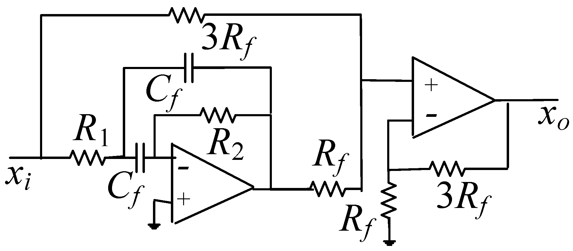
To control the instability, a time delay circuit was adopted in the voltage loop. This circuit was composed of two series filters, as indicated in Figure 1. The filter is shown in Figure 2. Because the input is a periodic rectified voltage, the double averaging method was an appropriate tool [14,15]. The first averaging process resulted in a set of nonlinear equations describing the dynamics of the main circuit and the control circuit [16]. This is a routine process, which can be found in almost every power converter. The aim of this process is to obtain an averaged model, which reflects the dynamics of the converter, only far below the switching frequency. In DC-DC converters, the input voltage is not time varying, and therefore the averaged model is used to design the controller after linearization. On the other hand, in PFC converters, the input voltage is a periodic rectified waveform, and the linearization of the averaged model cannot predict bifurcation in the converter. As a result, the bifurcation analysis must depend on the second averaging process. The second averaging process studies the set of nonlinear equations in the first averaging process with the harmonic balance method [17,18,19,20,21,22].

2.1. Main Circuit

For the main circuit, the relationship between the output voltage and the voltage control loop must be derived.
The converter can be described by
{ d i L d t = 1 L ( v i n v o ) d v o d t = 1 C ( i L v o R )
when the switch is on, and
{ d i L d t = 1 L v i n d v o d t = 1 R C v o
when the switch is off. In this paper, the instability in the line frequency was studied. Therefore, the dynamics in the switching frequency were omitted. Averaging over one switching period gives:
{ ( 1 d ) v o = v i n L d i L d t ( 1 d ) i L = C d v o d t + v o R
Combining the two equations in (1) gives:
C 2 d v o 2 d t = v 0 2 R + i L v i n L 2 d i L 2 d t
It is important to note that the dynamics of the inductor over one switching period are small enough to be omitted. This gives:
C 2 d v o 2 d t = v 0 2 R + i L v i n
On the other hand, in the OCC PFC converter, a resettable integrator replaced the current loop in the average current-controlled PFC converter. The advantage of the integrator is that it eliminates the perturbation of the input voltage within just one switching period. The introduction of the integrator also simplifies the structure and design process of the converter, as there is no need to design the current control loop. The only parameter in the integrator is the integral constant, which is normally equal to the switching period of the converter. Therefore, IR1150 needs fewer peripheral components compared with current-controlled PFC ICs. The operation principle of the converter gives:
R s i L ( t ) = v O A / M ( d )
where M ( d ) = v o / v i n and R s = R s 1 × 2.5 .
Therefore, one has:
i L ( t ) = v i n v O A / ( R s v o )
Substituting the input voltage v i n = V m | sin ω m t | into (5) gives:
C 2 d v o 2 d t = v 0 2 R + v O A R s v o V m 2 ( 1 cos 2 ω m t )
This equation determines the operation of output voltage v o and the voltage control loop voltage v O A .

2.2. Control Circuit

In the control circuit, the delay circuit takes the output voltage of the converter as its input. This architecture was different from the existing method in [7], where the output of the voltage control loop is adopted as the delay. The architecture in this paper is more practical in engineering.
The delay circuit was composed of two second-order filters. Each filter had the transfer function as follows:
G ( s ) = 1 2 R 1 C f s + R 1 R 2 C f 2 s 2 1 + 2 R 1 C f s + R 1 R 2 C f 2 s 2 .
A series of two filters introduced a delayed time τ . Details can be found in [9].
Apart from the delay circuit, the voltage control loop is a traditional control method. It takes the delayed output voltage as its input, and outputs a control voltage, v O A . The OA outputs a current, and its voltage is determined by the transfer function:
H ( s ) = g m ( 1 + s R g m C z ) s C z ,
where g m is the trans-conductance of the amplifier.
This gives:
C z d v O A d t = g m ( V r e f R f 2 ( v o η ( v o v o ( t τ ) ) ) R f 1 + R f 2 ) g m R g m C z R f 2 R f 1 + R f 2 d v o d t ,
where time variable t is omitted in output voltage v o ( t ) .
Equations (8) and (11) control the operation of the PFC converter. They are nonlinear and non-autonomous. In engineering, the force frequency ω m is fixed. The delay time τ is generally selected as the period of the rectified input voltage. Therefore, the feedback gain η is an important parameter in determining the stability of the PFC converter. The stability of the converter is studied by using the second average.

3. Stability of the OCC Boost PFC Converter

The output voltage of the OCC Boost PFC converter is almost constant in many applications. For simplification, we have:
v m R s v o = v m R s ( 1 + R f 1 / R f 2 ) V r e f .
The calculation error is small enough by doing so. Therefore, the OCC Boost PFC converter is controlled by:
{ C 2 d x 2 d t = x 2 R + V m 2 ( 1 cos 2 ω m t ) R s ( 1 + β ) V r e f y C z d y d t = g m ( V r e f ( x η ( x x ( t τ ) ) ) 1 + β ) g m R g m C z 1 1 + β d x d t ,
where y = v O A ( t ) , x = v o ( t ) , x ( t τ ) = v o ( t τ ) , β = R f 1 / R f 2 .
Equation (13) was derived through the first averaging process, so then the second averaging process must be applied to it to study its stability.
In the second averaging, any variable u ( t ) is expressed by:
u ( t ) u 0 + u 1 e j ω m t + u 1 e j ω m t + u 2 e j 2 ω m t + u 2 e j 2 ω m t ,
where:
u k = ω m 2 π t 2 π ω m t u ( τ ) exp ( j k ω m τ ) d τ   ( k = 0 , ± 1 , ± 2 ) .
Furthermore, u 1 = u 1 * = u 1 r j u 1 i , and u 2 = u 2 * = u 2 r j u 2 i , where * stands for complex conjugate.
Taking the second averaging on Equation (13) gives:
{ C 2 d d t ( x 0 2 + 2 x 1 r 2 + 2 x 1 i 2 + 2 x 2 r 2 + 2 x 2 i 2 ) + 1 R ( x 0 2 + 2 x 1 r 2 + 2 x 1 i 2 + 2 x 2 r 2 + 2 x 2 i 2 ) = V i n 2 ( y 0 y 2 r ) R s ( 1 + β ) V r e f C z d d t y 0 = g m ( V r e f ( x 0 η ( x 0 x 0 ( t τ ) ) ) 1 + β ) g m R g m C z 1 1 + β d d t x 0 ,
{ C 2 d d t ( x 0 x 1 + x 1 r x 2 r + x 1 i x 2 i + j ( x 1 r x 2 i x 1 i x 2 r ) ) + ( j ω m C 2 + 1 R ) ( x 0 x 1 + x 1 r x 2 r + x 1 i x 2 i + j ( x 1 r x 2 i x 1 i x 2 r ) ) = V i n 2 R s ( 1 + β ) V r e f ( y 1 2 y 1 * 4 ) C z ( d d t y 1 + j ω m y 1 ) = g m 1 1 + β ( x 1 η ( x 1 x 1 ( t τ ) ) ) g m R g m C z 1 1 + β ( d d t x 1 + j ω m x 1 ) ,
{ C 2 d d t ( ( x 1 * ) 2 + 2 x 0 x 2 ) + ( j ω m C + 1 R ) ( ( x 1 * ) 2 + 2 x 0 x 2 ) = V i n 2 R s ( 1 + β ) V r e f ( y 2 1 2 y 0 ) C z ( d d t y 2 + j 2 ω m y 2 ) = g m ( x 2 η ( x 2 x 2 ( t τ ) ) ) 1 + β g m R g m C z 1 1 + β ( d d t x 2 + j 2 ω m x 2 )
These equations represent the DC component, the first harmonic component and the second harmonic component of the OCC Boost PFC converter, respectively.
In these equations, the gain η is an important parameter. To stabilize the converter, the feedback gain η must stabilize all these harmonics.

3.1. DC Component

In studying the DC component, the first harmonic and the second harmonic can be omitted. This results in the following:
{ C x 0 d x 0 d t + 1 R ( x 0 2 ) = V i n 2 R s ( 1 + β ) V r e f y 0 C z d d t y 0 = g m ( V r e f ( x 0 η ( x 0 x 0 ( t τ ) ) ) 1 + β ) g m R g m C z 1 1 + β d d t x 0
To study this nonlinear time delay equation, the equilibrium point ( X 0 , Y 0 ) must be obtained. Then, linearization in the vicinity of the equilibrium point gives:
{ d x ^ 0 d t = V i n 2 R s C X 0 ( 1 + β ) V r e f y ^ 0 2 x ^ 0 R C d y ^ 0 d t = g m C z 1 1 + β ( x ^ 0 η ( x ^ 0 x ^ 0 ( t τ ) ) ) g m R g m 1 1 + β d d t x ^ 0
The stability of this delay system is determined by a quasi-polynomial:
det ( J 0 + J τ exp ( s τ ) s I 2 × 2 )
where J 0 is the Jacobian matrix with respect to the non-delayed states and J τ is the Jacobian matrix with respect to the delayed states. The stability of the DC component gives a boundary of feedback gain. The calculation of the boundary is complicated; however, an approximation method can be found in [7].

3.2. The Second Harmonic Component

It is practical to consider that the DC component and the second harmonic component are constant in the analysis of the first harmonic component in the existing literature. In a normal PFC converter without delay circuit, the first harmonic component is much smaller than the DC component and the second harmonic component. Therefore, Equations (14) and (16) can be written as:
{ C 2 d d t ( x 0 2 + 2 x 2 r 2 + 2 x 2 i 2 ) + 1 R ( x 0 2 + 2 x 2 r 2 + 2 x 2 i 2 ) = V i n 2 R s ( 1 + β ) V r e f ( y 0 y 2 r ) C z d d t y 0 = g m ( V r e f 1 1 + β x 0 ) g m R g m C z 1 1 + β d d t x 0
{ C 2 d d t ( 2 x 0 x 2 ) + ( j ω m C + 1 R ) ( 2 x 0 x 2 ) = V i n 2 R s ( 1 + β ) V r e f ( y 2 1 2 y 0 ) C z ( d d t y 2 + j 2 ω m y 2 ) = g m 1 1 + β x 2 g m R g m C z 1 1 + β ( d d t x 2 + j 2 ω m x 2 )
By making all time-derivatives in these equations equal to zero, one obtains:
{ 1 R ( x 0 2 + 2 x 2 r 2 + 2 x 2 i 2 ) = V i n 2 ( y 0 y 2 r ) R s ( 1 + β ) V r e f g m ( V r e f 1 1 + β x 0 ) = 0
{ ( j ω m C + 1 R ) ( 2 x 0 x 2 ) = V i n 2 ( y 2 y 0 / 2 ) R s ( 1 + β ) V r e f j 2 ω m C z y 2 = g m 1 1 + β x 2 j 2 ω m g m R g m C z 1 1 + β x 2
From theses equations, one obtains the steady-state DC component:
x 0 = ( 1 + β ) V r e f
and the second harmonic component is zero. With the DC component and the second harmonic component, one can study the stability of the first harmonic component.

3.3. The First Harmonic Component

By taking the DC component and the second harmonic component as constant, and noting that the delay time is the period of the rectified input voltage, one can obtain the following equation controlling the first harmonic component:
{ ( j ω m C 2 + 1 R ) x 0 x 1 = V i n 2 R s ( 1 + β ) V r e f ( y 1 r 4 + j 3 y 1 i 4 ) j ω m C z y 1 = g m 1 1 + β ( 1 2 η ) x 1 j g m R g m ω m C z 1 1 + β x 1
Isolating the real and imaginary part of these equations, one obtains:
( x 1 r x 1 i ) = V m 2 4 R s ( 1 + β ) V r e f ( 1 R 2 + ω m 2 C 2 4 ) x 0 2 × ( x 0 R 3 ω m C ( x 0 ) 2 ω m C ( x 0 ) 2 3 ( x 0 R ) ) ( y 1 r y 1 i )
( y 1 r y 1 i ) = 1 C z ω m ( g m R g m C z ω m 1 + β ( 1 2 η ) g m 1 + β ( 1 2 η ) g m 1 + β g m R g m C z ω m 1 + β ) ( x 1 r x 1 i )
These equations describe the transfer function of the first harmonic in the main circuit and the control circuit. Therefore, one can obtain the following total transfer function:
M = g m C z ω m ( 1 + β ) ( R g m C z ω m ( 1 2 η ) 1 2 η R g m C z ω m ) × V m 2 4 R s ( 1 + β ) V r e f ( 1 R 2 + ω m 2 C 2 4 ) x 0 2 × ( x 0 R 3 ω m C x 0 2 ω m C x 0 2 3 x 0 R )
If the converter operates in a normal stable mode, the first harmonic must be zero. This can be met when all eigenvalues of M lie within the unit circle. Apparently, the gain η determines eigenvalues.

3.4. Stability Boundary of Gain η

The gain η determines the stability of both the DC component and the first harmonic component in Equations (19) and (28). They together give the stability boundary of gain η .

4. Results

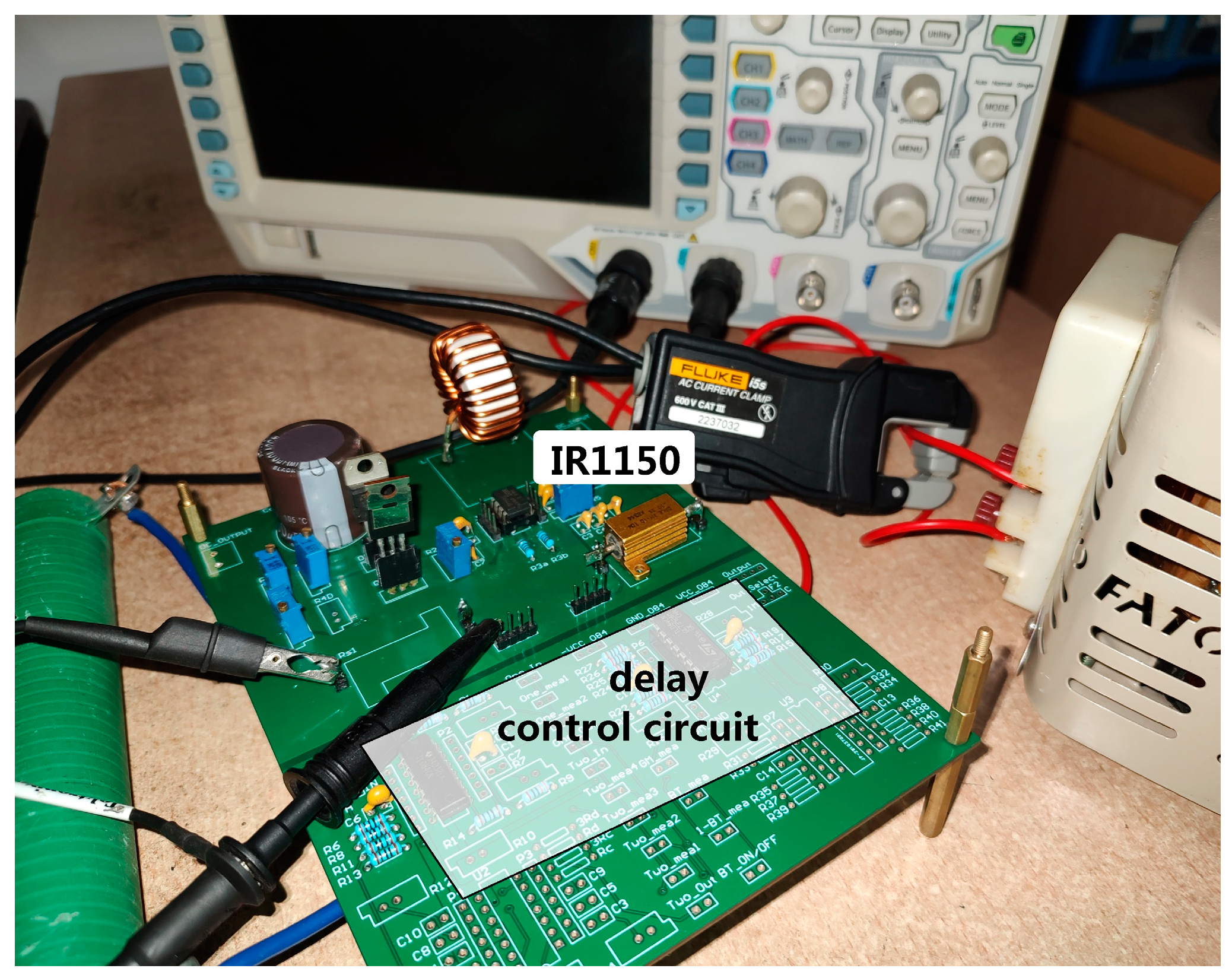
An experimental prototype was implemented with an OCC Boost PFC IC IR1150, and is shown in Figure 3. In the experimental circuit, the period of the OCC was 15 μ s , the line frequency was 100π rad/s, the inductance was 2 mH, the output capacitance of the main circuit was 100 μ F , the load resistance was 1600 Ω, and the parameters in the control circuit were R f 1 = 849   k Ω , R f 2 = 37.3   k Ω , R g m = 10.25   k Ω , C z = 32   n F , C p = 32   p F , V r e f = 7   V , R s = 0.645   Ω , g m = 40   μ s . The delay time in the delay circuit were 10 ms.

4.1. Calculated and Simulation Stability Boundary of Gain

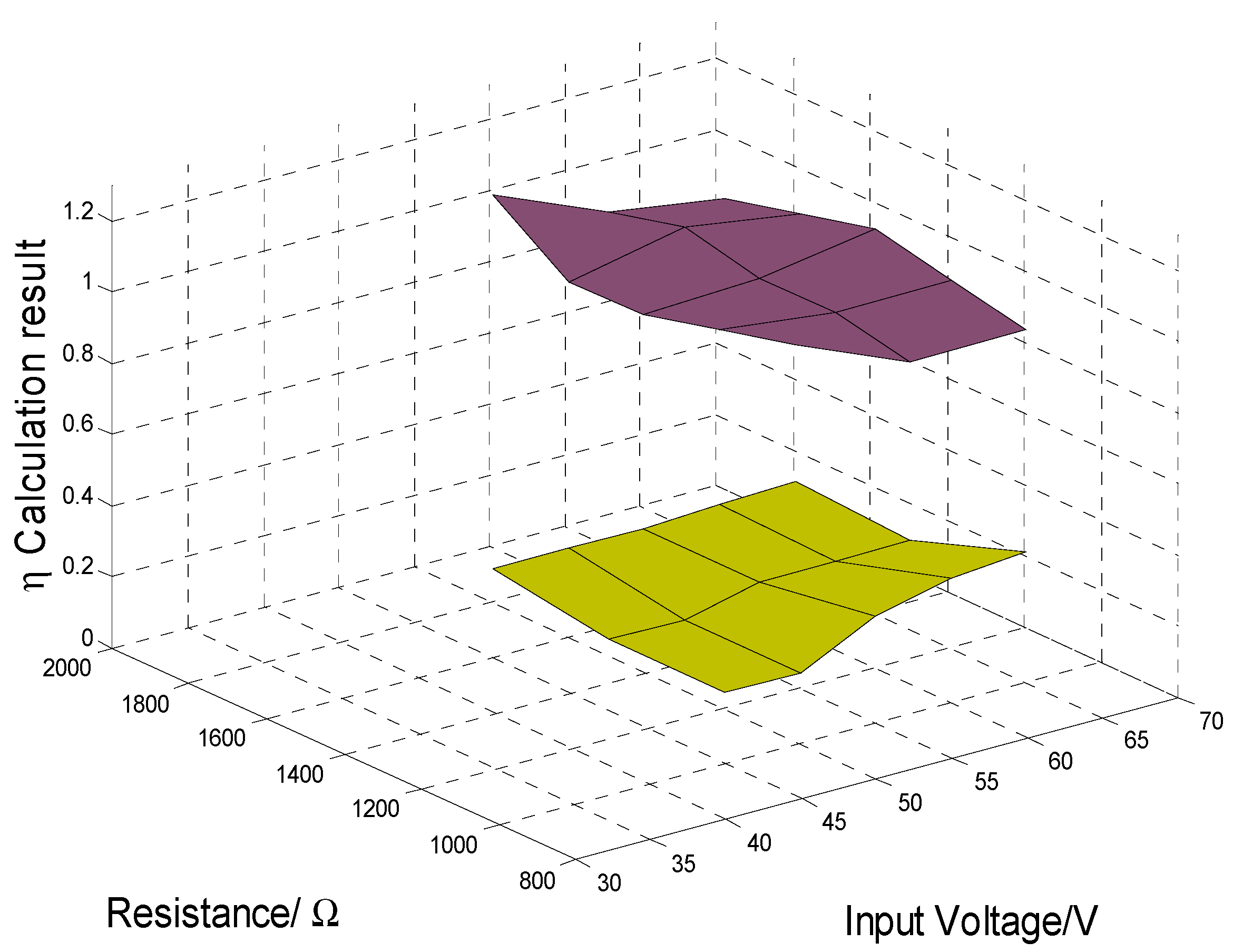
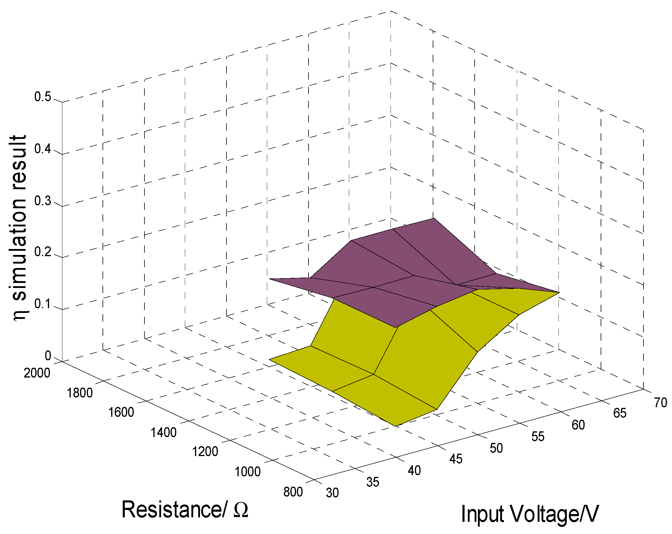
The stability boundary of the feedback gain under various input voltages and load resistances was between the two surfaces shown in Figure 4 based on Equations (19) and (28). MATLAB simulation was performed to determine the stability boundary of the feedback gain, and the result is shown in Figure 5. The error was caused by the non-ideal components in the circuit and the approximation in calculation.

4.2. Simulation Results

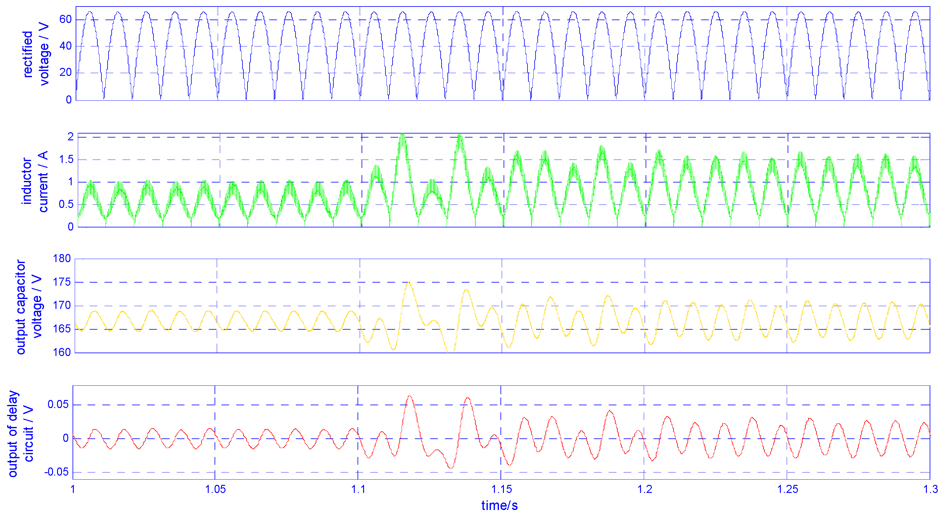
For an input voltage of 66 V and a feedback gain selected as 0.25, the simulation result is shown in Figure 6. Before activating the delay circuit at t = 1   s , the converter exhibited line frequency period-doubling bifurcation. After activating the method, the converter entered transience, and then recovered to stable operation. Because of the limit of space, only transience is shown in Figure 6, and the recovered stable operation is not shown. However, in the following subsection, experimental waveforms showed the recovered stable operation.

4.3. Improvement of PF

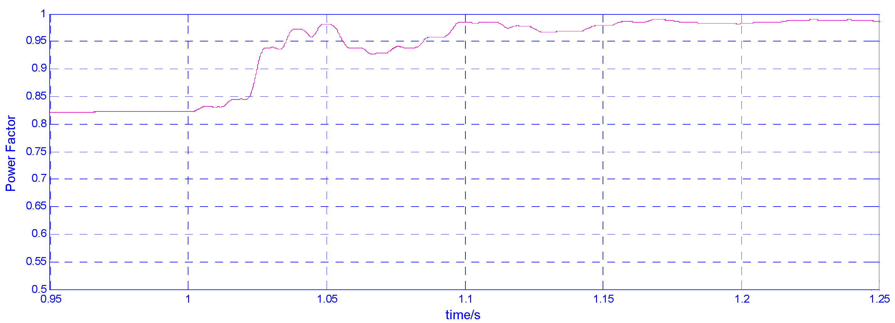
Figure 7 shows the Power Factor before and after activating the delay circuit. It can be seen that before activating the delay circuit the PF was only 0.82, and after activating the delay circuit the PF became as high as 0.99. This was consistent with the simulation result in [7]. Therefore, PF can be improved to 0.99 by appropriately selecting the feedback gain in the delay circuit. As a comparison, the notch filter method in [6] increased PF from 0.71 (THD =99%) to 0.99 (THD = 14%). Both methods can improve PF by eliminating bifurcation.

4.4. Dynamics Performances in Front of Load Change

Figure 8 shows dynamics performances of the converter subject to the proposed time delay circuit in front of the load change. The load resistance changed from 1600 Ω to 800 Ω and the converter recovered to stable operation after transient. It can be noted that the output of the delay circuit was small enough before and after the step change of load resistance. As a comparison, the notch filer method in [6] was also stable before load changes.

4.5. Experimental Results

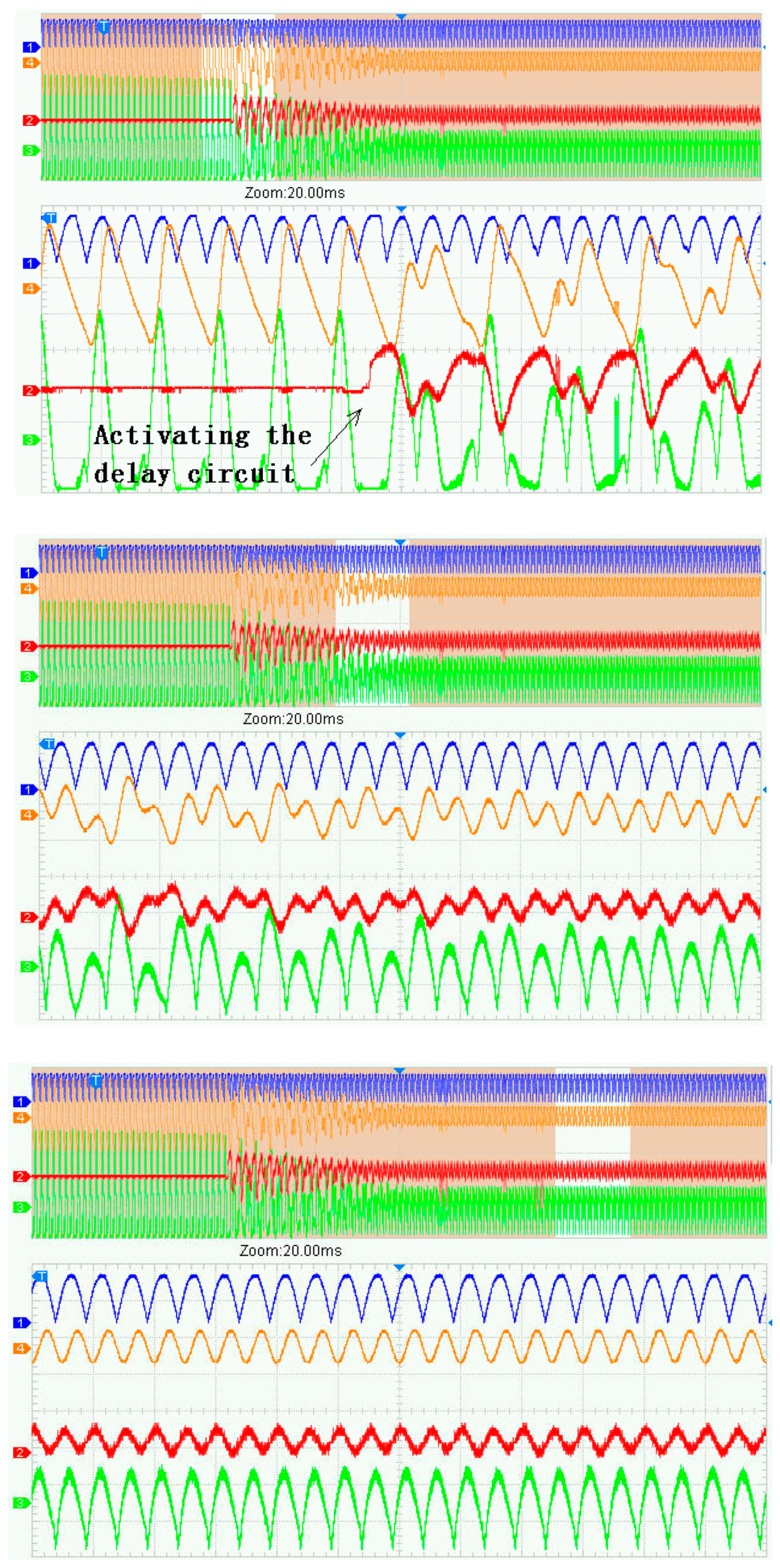
Figure 9 shows the overall and zoomed-in experimental waveforms before and after activating the delay circuit method. Before activating the method, the OCC Boost PFC converter exhibited bifurcation in the line frequency, and the output ripple was large. After activating the method, the converter entered transience, and then recovered to the stable operation with the frequency of the output ripple equal to the frequency of the rectified input voltage. This was consistent with the simulation waveforms. The converter needed a long time to recover to stable operation because of the limited bandwidth of the voltage loop. This also existed in the notch filter method in [6].

5. Conclusions

The OCC PFC converter has only one voltage loop, which may exhibit unstable operation as the result of bifurcation in the line frequency when the load is light and the output capacitor is small. The bifurcation decreases the PF and results in a large output voltage ripple. To stabilize the converter, an analog delay circuit based on filters is proposed in this paper. Simulation results and an experimental prototype verified the delay circuit method. The only parameter needed in the method was the feedback gain, which was computed through the double averaging method.
The delay control method stabilizes the unstable orbit embedded in an attractor. From the experimental waveforms, one can see that the output of the delay circuit was small enough compared the control voltage in the converter. Therefore, the delay circuit did not affect the normal operation of the OCC Boost PFC converter.
The stabilization of the converter by the delay control circuit can improve the PF to 0.99, and decrease the reactive power. After activating the delay circuit, the output capacitor voltage ripple became smaller, and the performance and lifetime of the electrolytic capacitor could be improved. Therefore, the delay control circuit is an effective method to stabilize the OCC PFC converter.

Author Contributions

Methodology, simulation experiment and writing—original draft preparation, R.Z., W.M. and L.W.; writing—review and editing, W.M., J.D. and G.Y. All authors have read and agreed to the published version of the manuscript.

Funding

This research was funded the National Science Foundation of China (NSFC, Grant No. 81527806, No. 62001169) and the Fundamental Research Funds for the Central Universities, China (No. 2019CDYB-8).

Data Availability Statement

The data used to support the findings of the study are available within the article.

Conflicts of Interest

The authors declare no conflict of interest.

References

  1. Chu, G.; Tse, C.K.; Wong, S.C. Line-frequency instability of PFC power supplies. IEEE Trans. Power Electron. 2009, 24, 469–482. [Google Scholar] [CrossRef]
  2. Zhang, R.; Ma, W.; Wang, L.; Hu, M.; Cao, L.; Zhou, H.; Zhang, Y. Line frequency instability of One-Cycle-Controlled boost power factor correction converter. Electronics 2018, 7, 203. [Google Scholar] [CrossRef]
  3. El Aroudi, A.; Orabi, M.; Haroun, R.; Martínez-Salamero, L. Asymptotic slow-scale stability boundary of PFC ac-dc power converters: Theoretical prediction and experimental validation. IEEE Trans. Ind. Electron. 2011, 58, 3448–3460. [Google Scholar] [CrossRef]
  4. Wang, F.; Zhang, H.; Ma, X. Analysis of slow-scale instability in boost PFC converter using the method of harmonic balance and floquet theory. IEEE Trans. Circuits Syst. I 2010, 57, 405–414. [Google Scholar] [CrossRef]
  5. Ma, W.; Wang, M.; Liu, S.; Li, S.; Yu, P. Stabilizing the average current-mode-controlled boost PFC converter via washout-filter-aided method. IEEE Trans. Circuits Syst. II Exp. Briefs 2011, 58, 595–599. [Google Scholar] [CrossRef]
  6. El Aroudi, A.; Haroun, R.; Cid-Pastor, A.; Martinez-Salamero, L. Suppression of Line Frequency Instabilities in PFC AC-DC Power Supplies by Feedback Notch Filtering the Pre-Regulator Output Voltage. IEEE Trans. Circuits Syst. I Regul. Pap. 2013, 60, 796–809. [Google Scholar] [CrossRef]
  7. El Aroudi, A.; Orabi, M. Dynamics of PFC power converters subject to time-delayed feedback control. Int. J. Circuit Theory Appl. 2012, 40, 15–35. [Google Scholar] [CrossRef]
  8. Pyragas, K. Continuous control of chaos by self-controlling feedback. Phys. Lett. A 1992, 170, 421–428. [Google Scholar] [CrossRef]
  9. Maia, D.; Kurths, J.; Yanchuk, S. Stabilization of synchronous equilibria in regular dynamical networks with delayed coupling. Nonlinear Dyn. 2023, 111, 7377–7390. [Google Scholar] [CrossRef]
  10. Mohammadpour, M.; Abdelkefi, A.; Safarpour, P.; Gavagsaz-Ghoachani, R.; Zandi, M. Controlling chaos in bi-stable energy harvesting systems using delayed feedback control. Meccanica 2023, 58, 587–606. [Google Scholar] [CrossRef]
  11. Jafaripournimchahi, A.; Cai, Y.F.; Wang, H.; Sun, L. Environmental Analyses of Delayed-Feedback Control Effects in Continuum-Traffic Flow of Autonomous Vehicles. Sustainability 2022, 14, 11292. [Google Scholar] [CrossRef]
  12. Ma, W.; Wang, L.; Zhang, R.; Li, J.; Dong, Z.; Hu, M.; Liu, S. Hopf Bifurcation and Its Control in the One-Cycle Controlled Cuk Converter. IEEE Trans. Circuits Syst. II Express Briefs 2019, 8, 1411–1415. [Google Scholar] [CrossRef]
  13. Ma, W.; Zhang, R.; Wang, L.; Li, J.; Dong, Z.; Zhang, Y.; Hu, M. Stabilizing the buck converter with a first-order-filter-based time delay feedback controller. IEEE Access 2018, 6, 1967–1973. [Google Scholar] [CrossRef]
  14. Wong, S.C.; Tse, C.K.; Orabi, M.; Ninomiya, T. The method of double averaging: An approach for modeling power-factor-correction switching converters. IEEE Trans. Circuits Syst. 2006, 53, 454–462. [Google Scholar] [CrossRef]
  15. Orabi, M.; Haron, R.; Youssef, M.Z. Stability analysis of PFC converters with one-cycle control. In Proceedings of the 31st International Telecommunications Energy Conference, Incheon, Republic of Korea, 18–22 October 2009. [Google Scholar]
  16. Smedley, K.M.; Cuk, S. One-Cycle Control of Switching Converters. IEEE Trans. Power Electr. 1995, 10, 625–633. [Google Scholar] [CrossRef]
  17. Avrutin, V.; Zhusubaliyev, Z.T.; El Aroudi, A. Non-visible transformations of chaotic attractors due to their ultra-low density in AC-DC power factor correction converters. Nonlinear Dyn. 2020, 4, 2905–2924. [Google Scholar] [CrossRef]
  18. Avrutin, V.; Zhusubaliyev, Z.T.; Suissa, D.; El Aroudi, A. Non-observable chaos in piecewise smooth systems. Nonlinear Dyn. 2020, 99, 2031–2048. [Google Scholar] [CrossRef]
  19. Kim, S.; Bai, C.; Seok, H.; Choi, H.H.; Kim, M. Bridgeless Triple-Mode Resonant AC-DC Converter: Dynamic Modeling and Controls. IEEE Trans. Ind. Electron. 2020, 67, 4921–4933. [Google Scholar] [CrossRef]
  20. Caliskan, V.A.; Verghese, O.C.; Stankovic, A.M. Multifrequency averaging of DC/DC converters. IEEE Trans. Power Electron. 1999, 1, 124–133. [Google Scholar] [CrossRef]
  21. Khodabakhsh, J.; Moschopoulos, G. A Four-Switch Three-Phase AC-DC Converter with Galvanic Isolation. IEEE Trans. Power Electron. 2020, 35, 1699–1710. [Google Scholar] [CrossRef]
  22. Dorf, R.C.; Bishop, R.H. Modern Control Systems, 11th ed.; Pearson Education, Inc.: Upper Saddle River, NJ, USA; London, UK, 2008. [Google Scholar]
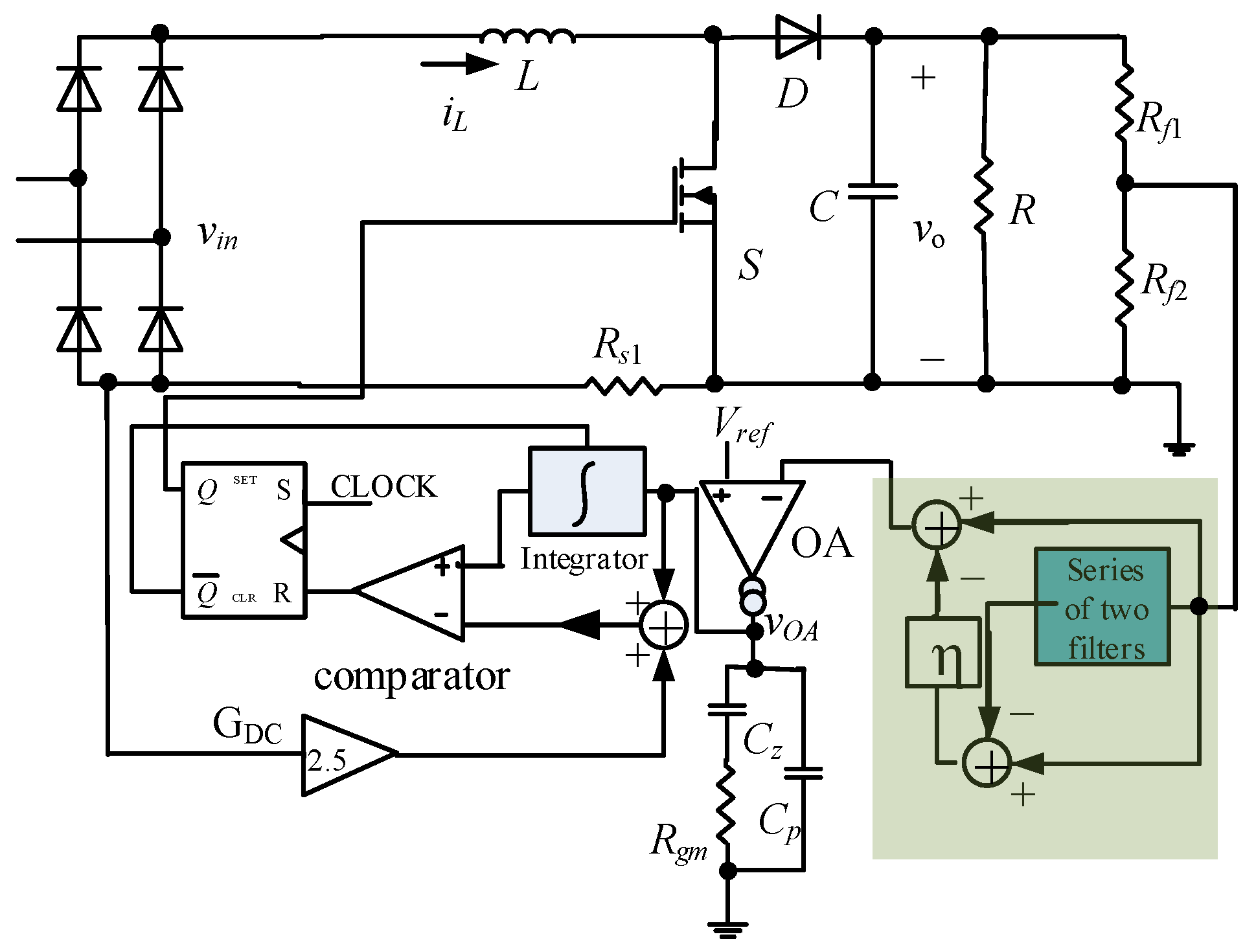
Figure 1. The OCC PFC converter.
Electronics 12 02291 g001
Figure 2. The filter in the time delay circuit.
Electronics 12 02291 g002
Figure 3. The experimental prototype.
Electronics 12 02291 g003
Figure 4. The calculated stability boundary.
Electronics 12 02291 g004
Figure 5. The simulation stability boundary.
Electronics 12 02291 g005
Figure 6. The simulation result.
Electronics 12 02291 g006
Figure 7. Improvement of PF.
Electronics 12 02291 g007
Figure 8. Dynamics performances before and after load change.
Electronics 12 02291 g008
Figure 9. The experimental waveforms. CH1: rectified input voltage 50 V/div. CH2: output of the delay circuit 100 mV/div. CH3: inductor current 0.5 A/div. CH4: output voltage ripple 2 V/div.
Electronics 12 02291 g009
Disclaimer/Publisher’s Note: The statements, opinions and data contained in all publications are solely those of the individual author(s) and contributor(s) and not of MDPI and/or the editor(s). MDPI and/or the editor(s) disclaim responsibility for any injury to people or property resulting from any ideas, methods, instructions or products referred to in the content.