
Investigation of Incident Angle Dependence of Single Event Transient Model in MOSFET

Abstract
:
1. Introduction
2. MOSFET Physics and SET Model
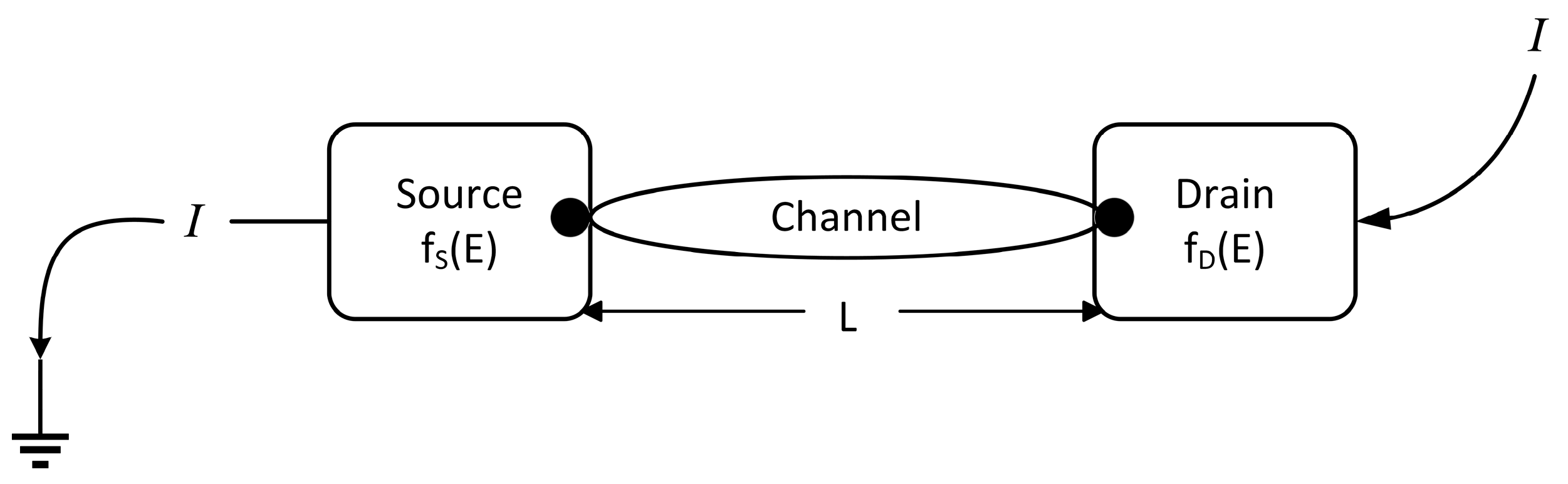
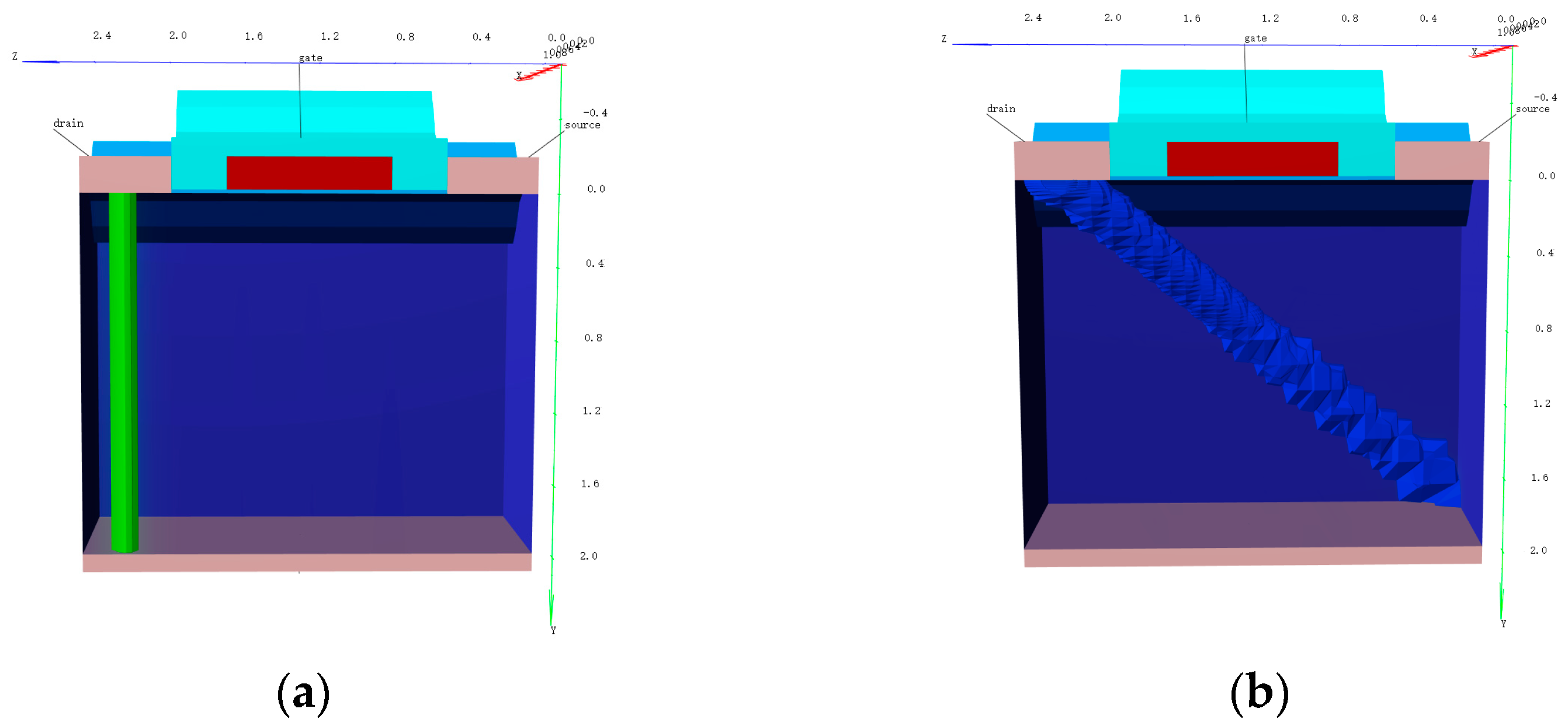
2.1. Transmission Theory
2.2. Physical Equations for Single Particle Incidence
2.3. SET Model
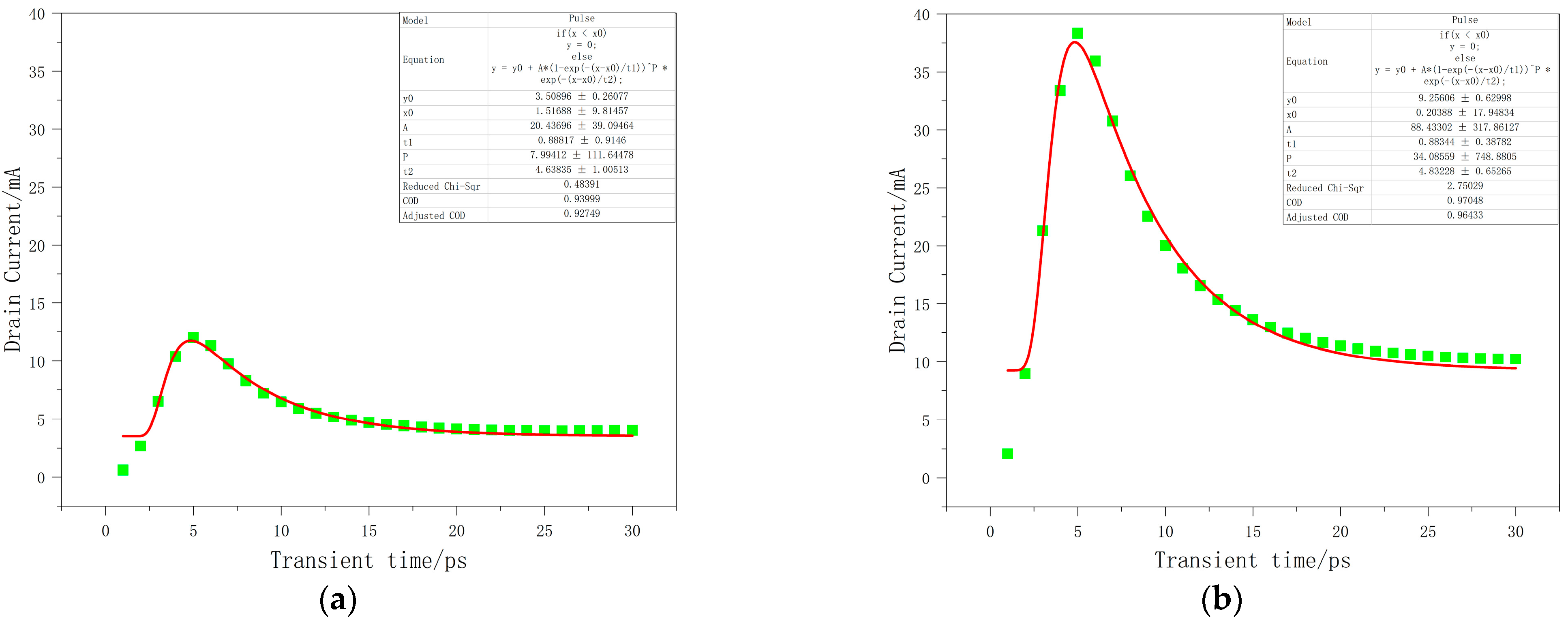
2.3.1. Double Exponential Function Based Model
2.3.2. Bias-Based SET Model
3. Results and Discussion
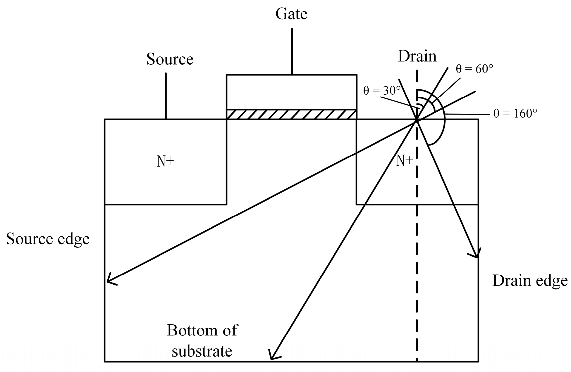
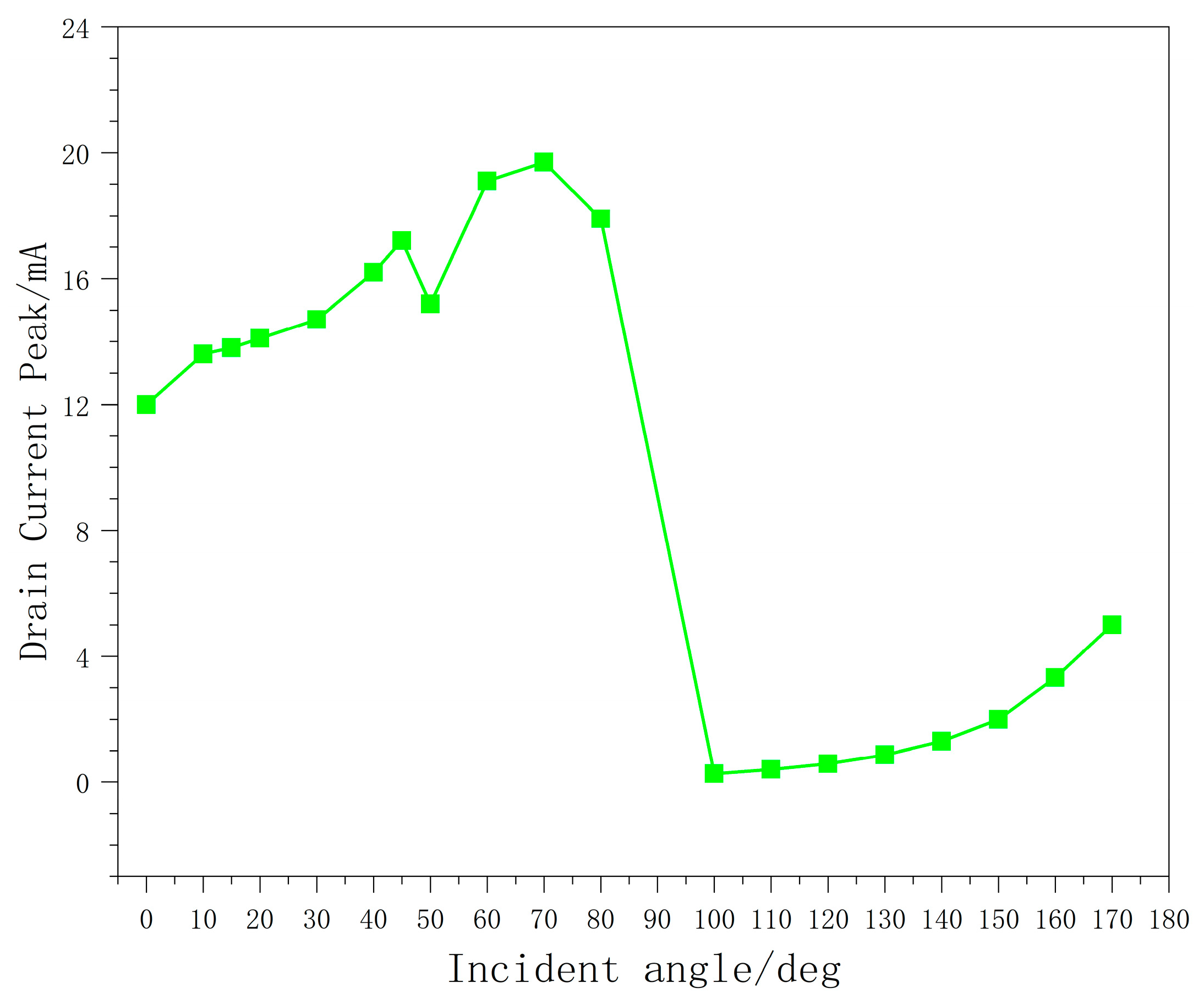
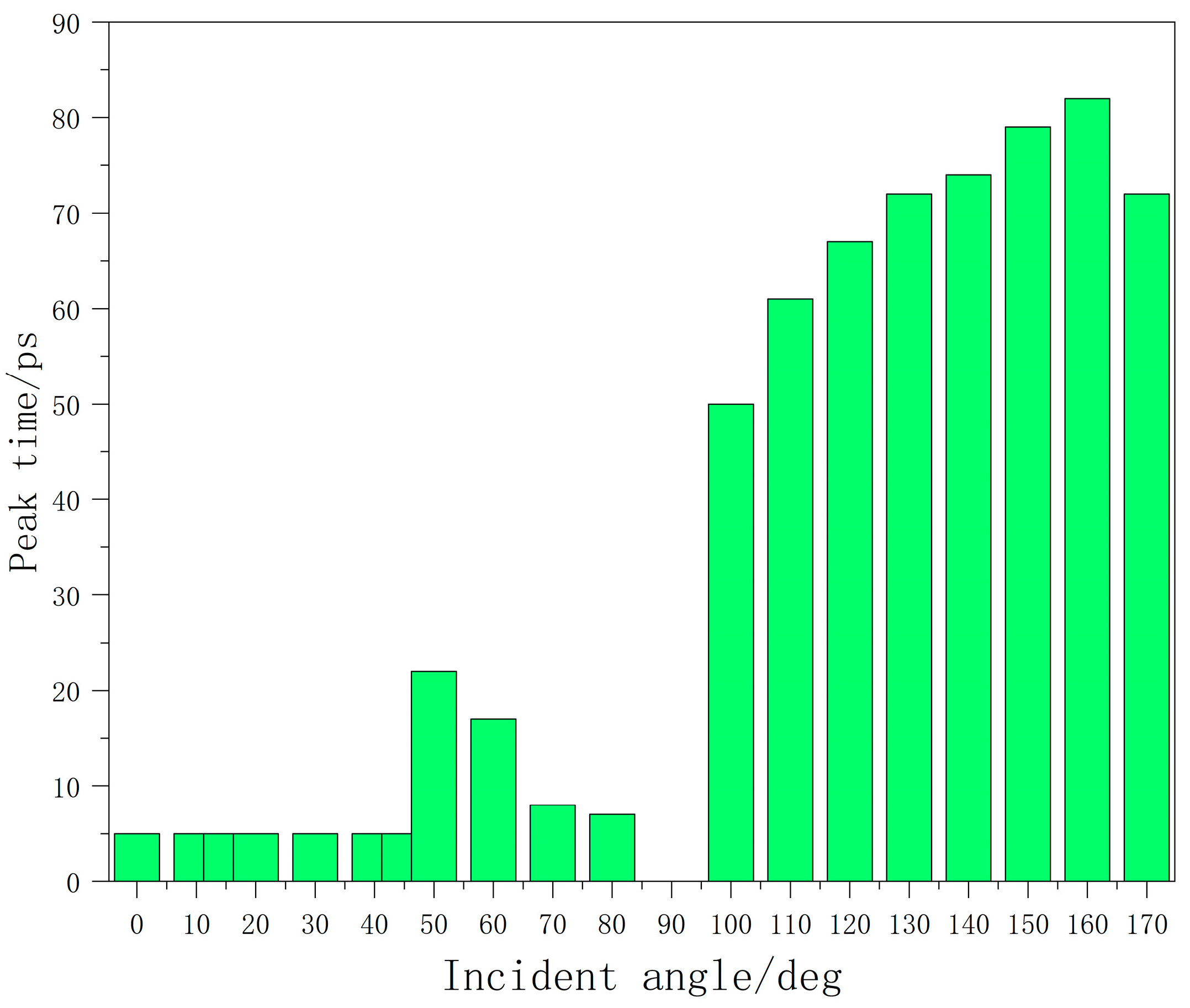
3.1. Incident Angle Dependence Investigation
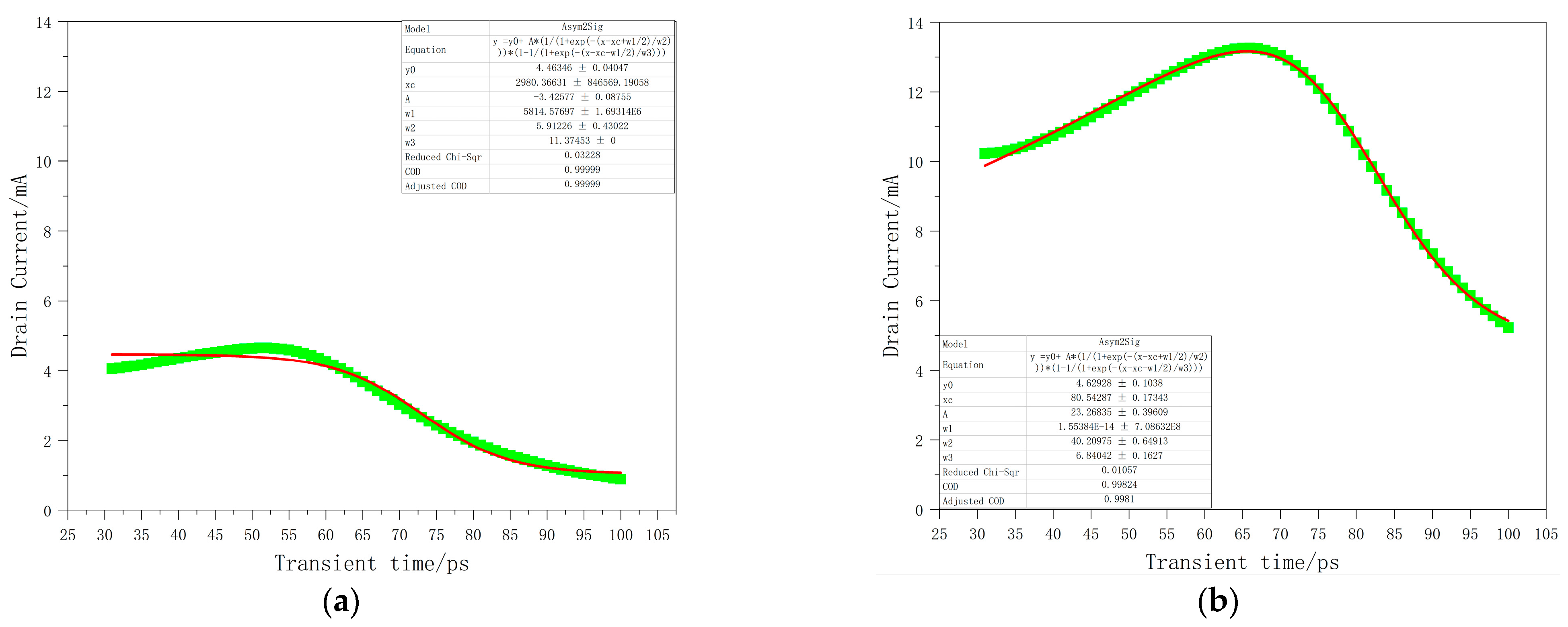
3.2. Double-Peaked SET Current Pulse Model
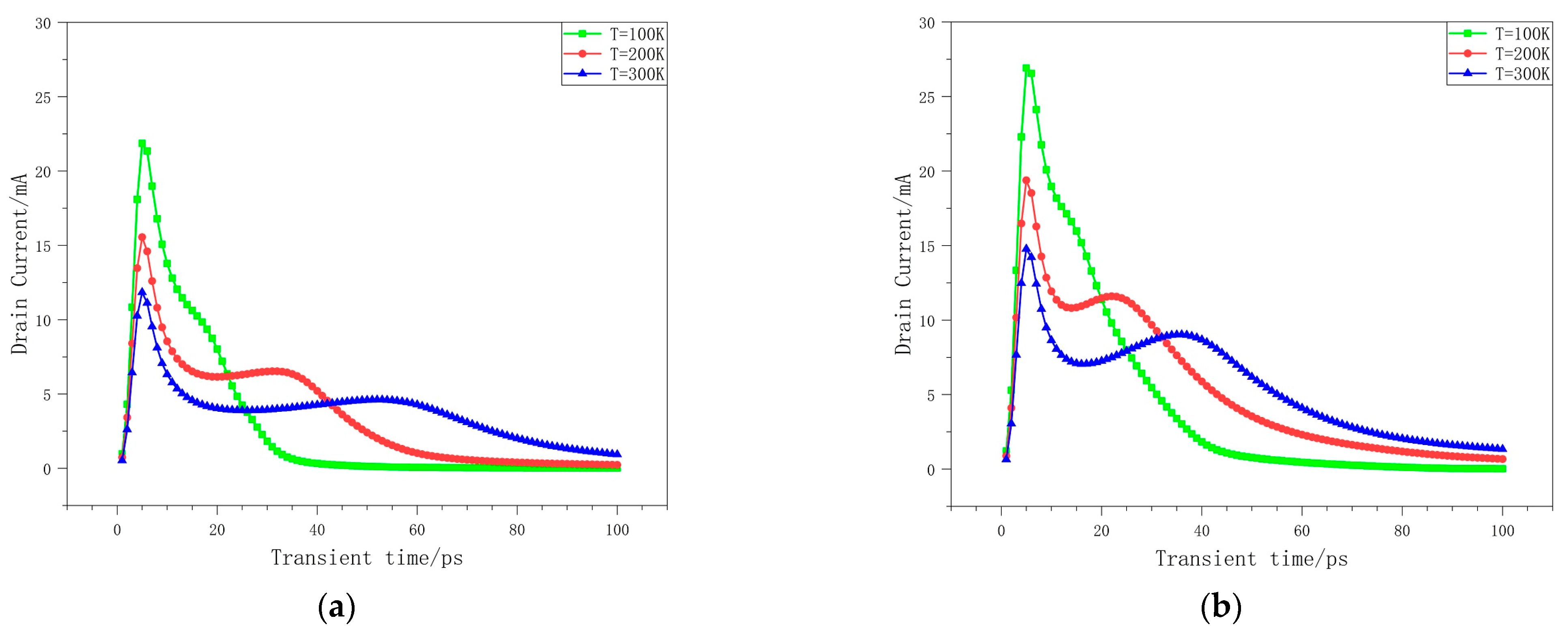
3.3. Incident Energy and Temperature Dependence Investigation
3.3.1. Incident Energy Dependence Investigation
3.3.2. Temperature Dependence Investigation
4. Conclusions
- (1)
- Most of the current research on the single event effect of semiconductor devices is limited to the computer simulation stage, and the conditions for conducting flight tests or ground simulation experiments do not allow for actual measurement data to be obtained yet.
- (2)
- With the continuous improvement of the semiconductor device fabrication process, the feature size of the device continues to decrease, so further research is needed in the future on the difficult issue of radiation-resistant reinforcement technology for small feature-size devices.
Author Contributions
Funding
Data Availability Statement
Acknowledgments
Conflicts of Interest
References
- Dodd, P.; Massengill, L. Basic mechanisms and modeling of single-event upset in digital microelectronics. IEEE Trans. Nucl. Sci. 2003, 50, 583–602. [Google Scholar] [CrossRef]
- Narasimham, B.; Bhuva, B.L.; Schrimpf, R.D.; Massengill, L.W.; Gadlage, M.J.; Amusan, O.A.; Holman, W.T.; Witulski, A.F.; Robinson, W.H.; Black, J.D.; et al. Characterization of Digital Single Event Transient Pulse-Widths in 130-nm and 90-nm CMOS Technologies. IEEE Trans. Nucl. Sci. 2007, 54, 2506–2511. [Google Scholar] [CrossRef]
- Baze, M.P.; Wert, J.; Clement, J.W.; Hubert, M.G.; Witulski, A.; Amusan, O.A.; Massengill, L.; McMorrow, D. Propagating SET Characterization Technique for Digital CMOS Libraries. IEEE Trans. Nucl. Sci. 2006, 53, 3472–3478. [Google Scholar] [CrossRef]
- Ferlet-Cavrois, V.; Paillet, P.; Gaillardin, M.; Lambert, D.; Baggio, J.; Schwank, J.R.; Vizkelethy, G.; Shaneyfelt, M.R.; Hirose, K.; Blackmore, E.W.; et al. Statistical Analysis of the Charge Collected in SOI and Bulk Devices Under Heavy lon and Proton Irradiation—Implications for Digital SETs. IEEE Trans. Nucl. Sci. 2006, 53, 3242–3252. [Google Scholar] [CrossRef]
- Ferlet-Cavrois, V.; Paillet, P.; McMorrow, D.; Fel, N.; Baggio, J.; Girard, S.; Duhamel, O.; Melinger, J.S.; Gaillardin, M.; Schwank, J.R.; et al. New Insights into Single Event Transient Propagation in Chains of Inverters—Evidence for Propagation-Induced Pulse Broadening. IEEE Trans. Nucl. Sci. 2007, 54, 2338–2346. [Google Scholar] [CrossRef]
- Ahlbin, J.R.; Massengill, L.W.; Bhuva, B.L.; Narasimham, B.; Gadlage, M.J.; Eaton, P.H. Single-Event Transient Pulse Quenching in Advanced CMOS Logic Circuits. IEEE Trans. Nucl. Sci. 2009, 56, 3050–3056. [Google Scholar] [CrossRef]
- Benedetto, J.M.; Eaton, P.H.; Mavis, D.G.; Gadlage, M.; Turflinger, T. Digital Single Event Transient Trends with Technology Node Scaling. IEEE Trans. Nucl. Sci. 2006, 53, 3462–3465. [Google Scholar] [CrossRef]
- Aneesh, Y.M.; Bindu, B. A Physics-Based Single Event Transient Pulse Width Model for CMOS VLSI Circuits. IEEE Trans. Device Mater. Reliab. 2020, 20, 723–730. [Google Scholar] [CrossRef]
- Baumann, R. Radiation-induced soft errors in advanced semiconductor technologies. IEEE Trans. Device Mater. Reliab. 2005, 5, 305–316. [Google Scholar] [CrossRef]
- Wirth, G.; Vieira, M.; Kastensmidt, F.L. Accurate and computer efficient modelling of single event transients in CMOS circuits. IET Circuits Devices Syst. 2007, 1, 137–142. [Google Scholar] [CrossRef]
- Wang, Z.; Zhou, W. An Evaluation Approach on SET Pulse Width. In Proceedings of the 2015 8th International Symposium on Computational Intelligence and Design (ISCID), Hangzhou, China, 12–13 December 2015; Volume 1, pp. 141–144. [Google Scholar]
- Black, D.A.; Robinson, W.H.; Wilcox, I.Z.; Limbrick, D.B.; Black, J.D. Modeling of Single Event Transients with Dual Double-Exponential Current Sources: Implications for Logic Cell Characterization. IEEE Trans. Nucl. Sci. 2015, 62, 1540–1549. [Google Scholar] [CrossRef]
- Francis, A.M.; Turowski, M.; Holmes, J.A.; Mantooth, H.A. Efficient modeling of single event transients directly in compact device models. In Proceedings of the 2007 IEEE International Behavioral Modeling and Simulation Workshop, San Jose, CA, USA, 20–21 September 2007; pp. 73–77. [Google Scholar]
- Messenger, G.C. Collection of Charge on Junction Nodes from Ion Tracks. IEEE Trans. Nucl. Sci. 1982, 29, 2024–2031. [Google Scholar] [CrossRef]
- Kauppila, J.S.; Ball, D.R.; Maharrey, J.A.; Harrington, R.C.; Haeffner, T.D.; Sternberg, A.L.; Alles, M.L.; Massengill, L.W. A Bias-Dependent Single-Event-Enabled Compact Model for Bulk FinFET Technologies. IEEE Trans. Nucl. Sci. 2019, 66, 635–642. [Google Scholar] [CrossRef]
- Mavis, D.G.; Eaton, P.H. SEU and SET Modeling and Mitigation in Deep Submicron Technologies. In Proceedings of the IEEE International Reliability Physics Symposium Proceedings, Phoenix, AZ, USA, 15–19 April 2007; pp. 293–305. [Google Scholar]
- Saremi, M.; Privat, A.; Barnaby, H.J.; Clark, L.T. Physically Based Predictive Model for Single Event Transients in CMOS Gates. IEEE Trans. Electron Devices 2016, 63, 2248–2254. [Google Scholar] [CrossRef]
- Aneesh, Y.M.; Sriram, S.R.; Pasupathy, K.R.; Bindu, B. An Analytical Model of Single-Event Transients in Double-Gate MOSFET for Circuit Simulation. IEEE Trans. Electron Devices 2019, 66, 3710–3717. [Google Scholar] [CrossRef]
- Kauppila, J.S.; Sternberg, A.L.; Alles, M.L.; Francis, A.M.; Holmes, J.; Amusan, O.A.; Massengill, L.W. A Bias-Dependent Single-Event Compact Model Implemented into BSIM4 and a 90 nm CMOS Process Design Kit. IEEE Trans. Nucl. Sci. 2009, 56, 3152–3157. [Google Scholar] [CrossRef]
- Rostand, N.; Martinie, S.; Lacord, J.; Rozeau, O.; Poiroux, T.; Hubert, G. Single Event Transient Compact Model for FDSOI MOSFETs Taking Bipolar Amplification and Circuit Level Arbitrary Generation into Account. In Proceedings of the International Conference on Simulation of Semiconductor Processes and Devices (SISPAD), Yokohama, Japan, 9–11 September 2019; pp. 1–4. [Google Scholar]
- Shih, C.-C.; Lambertson, R.; Hawley, F.; Issaw, F.; Mccollum, J.; Hamdy, E.; Sakurai, H.; Yuasa, H.; Honda, H.; Yamaoka, T.; et al. Characterization and modeling of a highly reliable metal-to-metal antifuse for high-performance and high-density field-programmable gate arrays. In Proceedings of the IEEE International Reliability Physics Symposium Proceedings, Dallas, TX, USA, 7–11 April 2002. [Google Scholar]
- Kauppila, J.S.; Massengill, L.W.; Ball, D.R.; Alles, M.L.; Schrimpf, R.D.; Loveless, T.D.; Maharrey, J.A.; Quinn, R.C.; Rowe, J.D. Geometry-Aware Single-Event Enabled Compact Models for Sub-50 nm Partially Depleted Silicon-on-Insulator Technologies. IEEE Trans. Nucl. Sci. 2015, 62, 1589–1598. [Google Scholar] [CrossRef]


| Incidence Angles/Deg | Exited Areas |
|---|---|
| 0, 10, 15, 20, 30, 40, 45 | Bottom of substrate |
| 50, 60, 70, 80 | Source edge |
| 100, 110, 120, 130, 140, 150, 160, 170 | Drain edge |
| Incident Angle/Deg | Primary Peak Current/mA | Inflection Current/mA | Secondary Peak Current/mA | Cumulative Charge/fC |
|---|---|---|---|---|
| 0 | 12 | 3.99 | 4.64 | 323 |
| 10 | 13.6 | 4.92 | 5.86 | 358 |
| 15 | 13.8 | 5.34 | 6.56 | 365 |
| 20 | 14.1 | 5.81 | 7.31 | 374 |
| 30 | 14.7 | 7.12 | 9.12 | 400 |
| 40 | 16.2 | 9.6 | 11.6 | 455 |
| 45 | 17.2 | 11.3 | 13 | 493 |
| 50 | 14.3 | 12.1 | 15.2 | 501 |
| 60 | 19.1 | - | - | 434 |
| 70 | 19.7 | - | - | 403 |
| 80 | 17.9 | - | - | 367 |
| 100 | 0.261 | - | - | 41.6 |
| 110 | 0.397 | - | - | 48.3 |
| 120 | 0.582 | - | - | 54.2 |
| 130 | 0.869 | - | - | 61.8 |
| 140 | 1.3 | - | - | 73 |
| 150 | 2 | - | - | 91.8 |
| 160 | 0.64 | 0.589 | 3.32 | 131 |
| 170 | 3.59 | 2.41 | 5 | 247 |
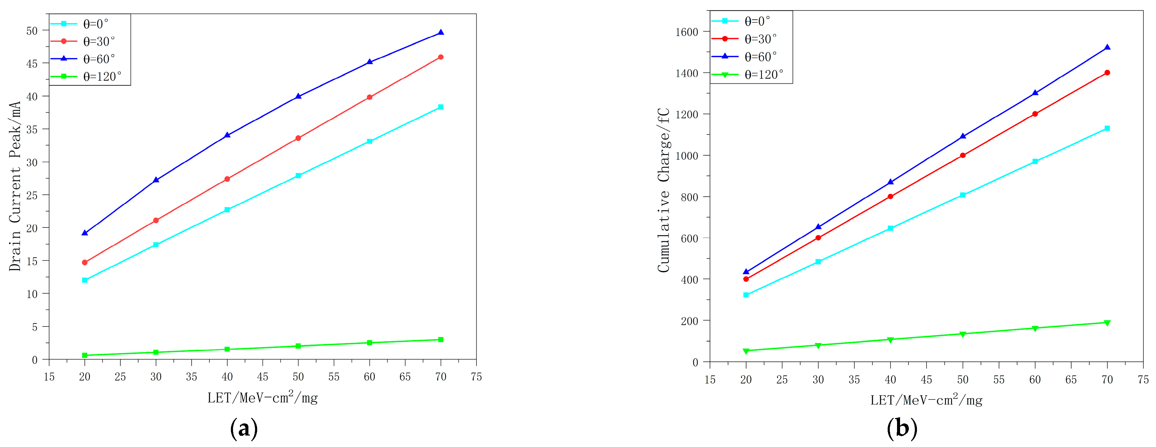
| Incidence Angles/Deg | LET/MeV-cm2/mg | Peak Current/mA | Charge Collection/fC |
|---|---|---|---|
| 0 | 20 | 12 | 323 |
| 30 | 17.4 | 484 | |
| 40 | 22.7 | 646 | |
| 50 | 27.9 | 807 | |
| 60 | 33.1 | 969 | |
| 70 | 38.3 | 1130 | |
| 30 | 20 | 14.7 | 400 |
| 30 | 21.1 | 600 | |
| 40 | 27.4 | 800 | |
| 50 | 33.6 | 999 | |
| 60 | 39.8 | 1200 | |
| 70 | 45.9 | 1400 | |
| 60 | 20 | 19.1 | 434 |
| 30 | 27.2 | 652 | |
| 40 | 34 | 869 | |
| 50 | 39.9 | 1090 | |
| 60 | 45.1 | 1300 | |
| 70 | 49.6 | 1520 | |
| 120 | 20 | 0.58 | 54.2 |
| 30 | 1.04 | 81.3 | |
| 40 | 1.52 | 108 | |
| 50 | 2.02 | 135 | |
| 60 | 2.51 | 163 | |
| 70 | 2.99 | 190 |
| Incidence Angles/Deg | Temperature/K | Peak Current/mA |
|---|---|---|
| 0 | 100 K | 21.9 |
| 200 K | 15.5 | |
| 300 K | 11.8 | |
| 30 | 100 K | 26.9 |
| 200 K | 19.4 | |
| 300 K | 14.8 |
Disclaimer/Publisher’s Note: The statements, opinions and data contained in all publications are solely those of the individual author(s) and contributor(s) and not of MDPI and/or the editor(s). MDPI and/or the editor(s) disclaim responsibility for any injury to people or property resulting from any ideas, methods, instructions or products referred to in the content. |
© 2023 by the authors. Licensee MDPI, Basel, Switzerland. This article is an open access article distributed under the terms and conditions of the Creative Commons Attribution (CC BY) license (https://creativecommons.org/licenses/by/4.0/).
Share and Cite
Zhang, F.; Wang, Y.; Liu, Y.; Wu, M.; Zhou, Z. Investigation of Incident Angle Dependence of Single Event Transient Model in MOSFET. Electronics 2023, 12, 2349. https://doi.org/10.3390/electronics12112349
Zhang F, Wang Y, Liu Y, Wu M, Zhou Z. Investigation of Incident Angle Dependence of Single Event Transient Model in MOSFET. Electronics. 2023; 12(11):2349. https://doi.org/10.3390/electronics12112349
Chicago/Turabian StyleZhang, Fan, Yibo Wang, Yi Liu, Minghu Wu, and Zilong Zhou. 2023. "Investigation of Incident Angle Dependence of Single Event Transient Model in MOSFET" Electronics 12, no. 11: 2349. https://doi.org/10.3390/electronics12112349