Abstract
A compact probe for charged particle imaging, with potential applications in source activity mapping and radio-guided surgery was designed and tested. The development of this technology holds significant implications for medical imaging, offering healthcare professionals accurate and efficient tools for diagnoses and treatments. To fulfill the portability requirements of these applications, the probe was designed for battery operation and wireless communication with a PC. The core sensor is a dual-layer CMOS SPAD detector, fabricated using 150 nm technology, which uses overlapping cells to produce a coincidence signal and reduce the dark count rate (DCR). The sensor is managed and interfaced with a microcontroller, and custom firmware was developed to facilitate communication with the sensor. The performance of the probe was evaluated by characterizing the on-board SPAD detector in terms of the DCR, and the results were consistent with the characterization measurements taken on the same chip samples using a purposely developed benchtop setup.
1. Introduction
Single photon avalanche diodes (SPADs) are semiconductor devices that are capable of detecting single photons thanks to the principle of avalanche multiplication. They are operated in what is known as Geiger mode, which involves biasing them above the breakdown voltage. SPADs find numerous applications in various fields, including photon counting, fluorescence spectroscopy, quantum optics, and LIDAR sensing [1,2,3,4,5]. However, SPADs can also exhibit high dark counts, i.e., events that occur even when no photons are present. This phenomenon, referred to as the dark count rate (DCR), can limit their sensitivity.
The APIX2/ASAP project, funded by the Italian Institute for Nuclear Physics (INFN) proposed to use CMOS SPADs for charged particle tracking. Its goal was to develop a new generation of layered avalanche detectors that reduce noise while keeping a low material budget. Two-tier arrays of SPADs are arranged face-to-face and vertically interconnected. By exploiting the low probability of simultaneous dark pulses occurring in the overlapping SPADs, the DCR is strongly reduced [6,7,8]. The target application of this sensor is charged particle tracking in low-rate and relatively clean environments, such as those found in experiments at future linear colliders [9]. Additionally, in response to the growing interest in the use of beta emitters as markers for radio-guided surgery (RGS) [10,11], a preliminary investigation was conducted to explore the potential of using the dual-layer sensor for imaging with radioactive beta sources [12,13,14].
Various portable solutions have been proposed for the localization of gamma or beta particles in RGS. One such solution for breast tumor localization with gamma rays is presented in [15]. It involves a scintillation crystal coupled to a silicon photomultiplier (SiPM), both enclosed in an aluminum housing. The probe also includes a pre-amplifier unit and is powered by a rechargeable battery. The output pulse is displayed on a computer through a BNC cable connected to a multi-channel analyzer. The pocket gamma camera (PGC), an intraoperative gamma camera designed for preoperative lymphoscintigraphy, is introduced in [16]. This handheld device boasts compact dimensions and a lightweight design, featuring an integrated display in the sensor unit. It is powered by a rechargeable battery. The PGC consists of a collimator matched with a scintillator, which is coupled to a SiPM via a light guide. The SiPM signals are read by an analog-to-digital converter (ADC), and an embedded system processes the data and displays the acquired image. Additionally, data can be transmitted to a computer through a universal serial bus (USB) interface. In [17], the MAGICS gamma camera is introduced as a dedicated solution for tumor localization during RGS. This gamma camera features a collimator and a scintillator coupled to an array of SiPMs. The readout system comprises a custom-designed chain of preamplifiers, shapers, and track-and-hold blocks, followed by an ADC. Data are saved and transferred to a USB port using an FPGA. Additionally, a Wi-Fi board is incorporated to enable wireless data transmission. In [18], an intraoperative probe designed for RGS in tumor resection involving beta particles is presented. The probe incorporates a scintillator tip that is shielded from side radiation, with the resulting light being guided by optical fibers to a photomultiplier tube (PMT). The readout electronics are housed in a compact box, which wirelessly connects to a monitor displaying the count rate.
This paper presents a portable detection probe that uses the dual-layer APIX2LF chip, which was developed as part of the APIX2/ASAP project. A microcontroller was carefully chosen to act as the interface between the sensor and the computer, and custom firmware was specifically designed for its operation. The power supply is provided by a rechargeable battery, and data can be sent to the computer by multiple protocols (USB, Wi-Fi, or Bluetooth), depending on the measurement requirements and conditions. The USB connection serves also as an alternative power supply and for battery recharge. It should be noted that the design, components, and firmware of the probe can be adapted for similar SPAD sensors. While the initial focus was on the APIX2LF chip, the underlying principles and methodologies employed in the design of the system can be extended to accommodate other SPAD sensors with similar characteristics.
The measurements presented in this work aimed to validate the proposed system by focusing on the breakdown voltage and dark count rate of SPAD arrays. These measurements were performed under different working conditions. In order to have a more accurate evaluation of the system, additional measurements using a radioactive source are being planned. The characterization process primarily concentrated on the fundamental aspects related to charged particle detection. As a result, certain features, such as light sensitivity and the linearity of light intensity conversion, which are of relevance in optical applications of SPAD sensors, were not included in the characterization process. As a matter of fact, in the dual-layer configuration, the two layers are face-to-face bonded so that the sensitive area of the SPAD lies in the inner part of the structure, resulting in the sensors being virtually insensitive to light. The dynamic range is primarily constrained by the SPAD dead time, which is approximately 100 ns in the considered devices. This allows for an operating dynamic range up to event rates of a few MHz in a single pixel, while the lower limit is determined by the DCR. The latter is by far more important than the maximum detectable event rate, as the expected event rate in applications such as RGS or lab source mapping is typically quite small, hardly exceeding 1 kHz/mm2.
As no measurements with a radioactive source were conducted in this study, direct comparison of the detection capabilities of the developed probe with other solutions is not possible. However, it is important to highlight the unique features of the above developed probe. Unlike many of the described systems, this probe performs most of the data processing on board, reducing the need for external processing, while providing a compact, operationally efficient, battery-powered solution. The need for additional space and power consumption is minimized since wireless data transfer capability is seamlessly integrated within the microcontroller. In addition, the developed probe offers full adaptability in data transmission options, providing users with the choice of Wi-Fi, Bluetooth, or USB for data transfer, thus allowing the probe to comply with different measurement scenarios and environments. The microcontroller can provide a fair degree of flexibility in the implementation of on-board functionalities, which may include counting, averaging, clustering and histogramming.
The organization of the paper is as follows. Section 2 describes the design of the printed circuit board (PCB) probe and the small carrier developed at the University of Padova for housing the sensor. Section 3 provides an overview of the APIX2LF chip and its characteristics. Section 4 discusses the firmware designed for the microcontroller to perform different types of measurements and the various protocols used for transferring data to the computer (Wi-Fi, Bluetooth, and USB). Finally, Section 5 presents the results of the chip characterization in dark conditions, validating the probe operation.
2. Battery-Operated, Wireless Probe
To ensure maximum flexibility in its use, the probe was designed to be powered either by cable or battery and to establish communication via wireless protocols. It was also designed as an all-in-one solution, with a microcontroller and all the reference circuits located on the same board as depicted in Figure 1 (left). A smaller housing case for the APIX2LF sensor was necessary for the miniaturized probe, and a two-stack PCB was designed and developed for this purpose at the University of Padova as shown in Figure 1 (right). The APIX2LF sensor is bonded on the top printed circuit board, while a commercial SiPM (Advansid ASD-NUV4S-P) with a BC-408 scintillator is mounted on the second printed board of the stack, located below the SPAD sensor. The following section provides a description of the different blocks making up the probe, which are schematically represented in Figure 2.
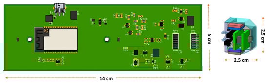
Figure 1.
Probe board prototype (left) and chip housing board (right).
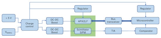
Figure 2.
Schematic diagram of components within the detection probe.
2.1. Microcontroller
Nowadays, the microcontroller market offers advanced solutions for signal processing, power management, and data transfer. Furthermore, with the rise of the Internet of Things (IoT), system on chips (SoCs) with built-in wireless solutions have emerged. One such SoC that has gained popularity for IoT applications is the ESP32, which is known for its low power consumption and wireless capabilities. Its dual-core processor and high-speed signal processing make it a suitable choice for real-time data processing. The CPU clock frequency can be adjusted to operate at 80 MHz, 160 MHz, or 240 MHz. Additionally, the ESP32 comes with integrated Wi-Fi and Bluetooth capabilities, allowing for easy connectivity to other devices and networks, making it a perfect fit for wireless data transfer applications.
The ESP32 WROVER module [19] was used for the probe design, which consists of the ESP32-D0WDQ6 chip, a PCB antenna for Wi-Fi and Bluetooth, 4 MB SPI flash memory, and 8 MB SPI Pseudo static RAM. The official ESP framework [20], which is based on C libraries and FreeRTOS® with built-in hardware acceleration, was used for this project. To achieve a balance between performance and battery management, the microcontroller is operated at a CPU clock frequency of 160 MHz. The ESP32 dual-core architecture allowed for the separate management of signal interface and data processing on one core, and data transfer on the other core.
2.2. Power Supply
To ensure continuous operation of the detection probe, a rechargeable battery was deemed the most appropriate option. To meet the 3.3 V power supply requirement of the microcontroller, a higher voltage was necessary. Additionally, it was crucial to select a battery compact in size that could provide enough energy to power the device continuously for several hours.
Lithium-ion (Li-Ion) batteries have emerged as the preferred option for consumer electronics due to their high energy density and slow discharge rate when not in use. Among them, lithium-ion polymer (LiPo) batteries offer additional advantages, such as lightweight construction, flexibility in shape, and slightly higher energy density compared to conventional Li-ion batteries [21]. LiPo batteries typically operate within a nominal voltage range of 3.6 V to 3.7 V, with a charging voltage around 4.2 V. To simplify the charging process and ensure safe operation, specialized integrated circuit (IC) battery charge controllers are readily available in the market. These controllers are designed to support a wide range of power supply voltages. The RS PRO LiPo rechargeable battery, with a charge capacity of 2.6 Ah and an operating temperature range of −20 °C and 60 °C [22], was chosen as the power source for the detection probe. Considering the power consumption of the probe, this battery can provide up to 10 hours of operating time when fully charged.
The widespread availability and popularity of the USB standard made it the chosen option for an alternative power supply serving both the board and battery recharge. To enable automatic switching between the USB and battery power, as well as battery power detection the circuit shown in Figure 3a was implemented. The probe uses the MCP73831 from Microchip as a battery management system (BMS), which offers charge and discharge management, along with overcharge protection, as illustrated in Figure 3b.
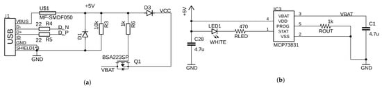
Figure 3.
Electrical circuit for choosing between battery or USB power supply (a) and for LiPo battery recharge (b).
2.3. ASD-NUV4S-P Readout Electronics
To have an independent triggering signal during measurements with a radioactive source, an Advansid ASD-NUV4S-P SiPM was integrated into the stacked carrier. This analog SiPM is based on p-on-n silicon technology and has a detection spectrum ranging from 350 nm to 900 nm, with peak efficiency at 420 nm. To enhance its detection efficiency, a BC-408 scintillator, covered by a mylar foil, was placed on top of the SiPM, which has 9340 cells with a pitch of 40 µm and a fill factor of 60%. The total effective area is mm2.
The inverting transimpedance amplifier (Figure 4) used to read the current from the SiPM consists of two stages: a common source stage and an emitter follower stage. The first stage is responsible for providing sufficient gain, while the second stage has a low output resistance, ensuring a wide bandwidth. The input current is converted into a voltage across the feedback resistor . The input transistor is biased at a constant current through the resistor , while the output transistor acts as an emitter follower with a load resistor . The values of the resistors and are chosen to provide the desired gain and bandwidth, respectively. The capacitor provides a high-frequency decoupling path to ground for the input stage.
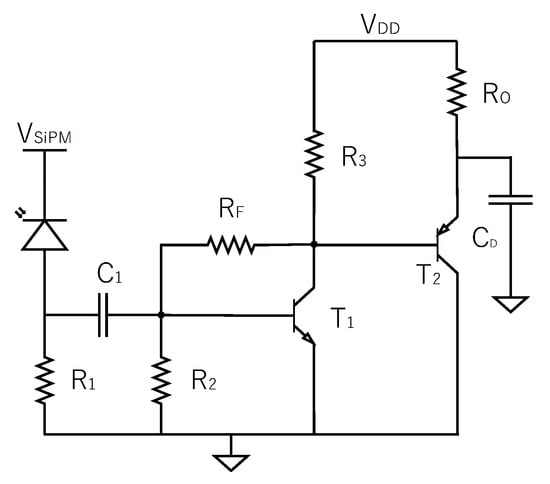
Figure 4.
Schematic circuit diagram of the transimpedance amplifier for the SiPM readout.
2.4. SPAD Biasing
In the characterization measurements described in [8,23,24,25], the bias voltage for the SPADs was provided by a power supply. However, to ensure the portability and wireless operation of the probe, it is necessary to extract the bias voltage for the SPADs and the SiPM from the battery itself.To achieve this, a DC-DC boost converter is used. The choice of the boost converter is based on the voltage source available on the board and the required bias voltages for the SPADs and SiPM. The LiPo battery supplies a minimum voltage of 3.7 V, while the SPADs are biased between 19 V and 21 V, and the SiPM requires a bias voltage between 27 V and 28 V.
The selected DC-DC boost converter is the TPS6104, manufactured by Texas Instruments [26]. This device is specifically designed to generate output voltages up to 28 V from a single-cell Li-Ion battery. It operates at a maximum switching frequency of 1 MHz and comes in a compact package. The schematic circuit diagram shown in Figure 5a illustrates how the output voltage of the DC-DC boost converter can be regulated to achieve the desired value for the APIX2LF and the Advansid SiPM by adjusting a trimmer ( = 200 kΩ). When employing switching power supplies with high peak currents and switching frequencies, it is crucial to carefully design the layout. To minimize ground shifts and noise, wide traces were used for signal connections, and a ground plane was incorporated.
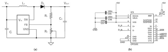
Figure 5.
Schematic circuit diagram of the DC-DC boost converter TPS61041 [26] (a) and for USB to UART bridge (b).
2.5. Supplementary Components
The ESP32 microcontroller features a dedicated UART interface that facilitates data exchange between the microcontroller and external devices. To establish a connection between the computer and the ESP32, a USB-to-UART bridge (Figure 5b) is used. This bridge serves the purpose of receiving binary data required for flashing the microcontroller memory with new applications, as well as enabling serial communication. The chosen USB-to-UART bridge IC for this implementation is the CP2102, developed by Silicon Labs. It integrates several essential components, including an internal clock, a voltage regulator, and a programmable ROM. The transfer rate of the UART communication can be adjusted according to the specific requirements of the application. The CP2102 chip supports transfer rates of up to 921,600 bits per second, allowing for fast and reliable data transmission, while the maximum baud rate for the flashing process is set to 115,200. The data received from the UART interface can be conveniently viewed and monitored using a terminal emulator.
To ensure compatibility between the APIX2LF V and the microcontroller signals at 3.3 V, the probe uses two 16-bit bus transceivers (SN74AVCA164245 by Texas Instruments) to act as a bridge between the two systems.
3. Dual-Layer CMOS SPAD Detector
The APIX2LF position-sensitive detector is a two-tier structure composed of 150 nm CMOS SPAD arrays that operates based on coincidence detection as shown in Figure 6. Each sensing element is equipped with its own readout electronics and quenching circuit, and the two layers are paired face-to-face to form a basic cell capable of producing a coincidence signal when a charged particle strikes two overlapping pixels simultaneously [6,8]. The two layers are fabricated separately on different chips and then vertically interconnected using micro bump bonding techniques. The DCR of the dual-layer pixel can be expressed as shown in the following equation:
where represents the coincidence time window and and are the dark count rate of the top and of the bottom SPAD, respectively. Assuming typical values for SPADs fabricated using a 150 nm CMOS technology of 1 kHz for both and [27], and a coincidence time window of 1 ns, the resulting DCR reduction calculated from (1) is more than five orders of magnitude. This significant reduction demonstrates the effectiveness of this structure in mitigating the effect of DCR on detection when compared to a single-layer detector [7].
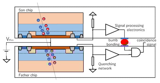
Figure 6.
Cross-section of two overlapped SPADs, forming a single cell of the APiX2LF detector crossed by a charged particle.
The APIX2LF dice dimensions are 6 mm × 5 mm, while its thickness is 150 µm. The chip contains four arrays of SPADs with different areas and signal processing circuits. As described in Section 2, a dual-layer chip is bonded on the top PCB of a two-stacked PCB carrier. To make the most efficient use of the available space on the carrier, only the two largest arrays (arrays 1 and 3) are connected and available for measurements on the APIX2LF. The characteristics of these two arrays are presented in Table 1. Shift registers are strategically placed around the arrays to select and enable/disable specific SPADs. A1 and A3 share the same row shift register but have different column shift registers. A thorough description of the chip and of the results of characterization can be found in [8,23].

Table 1.
Summary of the main characteristics of the APIX2LF detector arrays.
4. Firmware Design and Data Acquisition Framework
To provide flexibility in data transfer, three firmware versions were developed to support different communication interfaces: USB, Bluetooth, and Wi-Fi. The choice of firmware version depends on the specific measurement requirements and the operating environment. For scenarios where power consumption is a priority, Bluetooth is the preferred option, as it offers efficient power-saving features. However, Bluetooth has limitations in terms of bandwidth and coverage range compared to Wi-Fi. For situations where high-speed data transfer and longer-range coverage are required, Wi-Fi is the most suitable option. In cases where long and repeated measurements are performed and high-bandwidth data transmission is required, USB data transmission is the recommended choice, as it provides a reliable and stable connection, ensuring consistent data transfer.
4.1. APIX2LF Related Measurement Procedures
The SPAD features a binary operation, as it can be in either an on or off state depending on whether a particle has passed through it or not. To measure the signal from a SPAD, a time interval or frame is defined, during which the SPAD is enabled and ready for detection. This frame provides a result of 1 if an avalanche is triggered and 0 otherwise. By repeatedly performing the same measurement within the defined frame up to a preset total integration time (TIT), the results can be summed to obtain the rate of events. For the APIX2LF chip, a time frame of 100 μs was chosen based on the evaluation of the dark count rate range of a dual-layer chip [8]. The number of iterations (N) ranged from 10,000 to 300,000, resulting in a TIT of 1 to 30 s, respectively, depending on the measurement type. The general flowcharts relevant to the three different measurement procedures are shown in Figure 7 and Figure 8. They are referred to as follows:
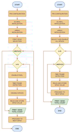
Figure 7.
Flowchart of “1-by-1” (left) and “AllON” (right) measurement procedure.
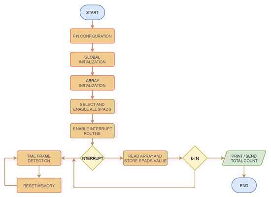
Figure 8.
Flowchart of SiPM-triggered measurement.
The three flowcharts share the first three blocks, while slightly differing in the remaining part. The common blocks concern the configuration of the pins of the microcontroller and the initialization of the chip under test. To provide flexibility and ease of use, predefined macros are used, allowing non-expert users to select the desired type of measurement, specify the array to be measured, or even choose a specific part of the array for characterization.
In the beginning, the general-purpose pins must be configured correctly to function as input or output pins of the microcontroller. Once pin configuration is complete, the system is ready for communication with the sensor. Global initialization is necessary for all input signals of the APIX2LF to ensure that they have a defined value. The “1-by-1” firmware measures and sends the count of each SPAD individually by selecting each row, one by one. The TIT is defined every time for a single SPAD, resulting in several hours to complete the measurement. In contrast, the “AllON” firmware measures all the pixels of an array or both arrays at once. The SPADs are enabled, and the detection frame is defined for all SPADs. Then, a complete readout of the array is performed. This operation is repeated for N frames to obtain a specific TIT, and the data corresponding to the total counts of the entire array are sent to the PC. This measurement takes only a few minutes to complete.
Another function was developed to use the SiPM signal as a trigger for reading the APIX2LF array with a radioactive source. As displayed in Figure 2, the SiPM signal is amplified and connected to a comparator to generate an interrupt signal for the microcontroller to read the SPAD array. Similar to the “AllON” measurement, all pixels are enabled at the beginning and remain enabled throughout the measurement. When the SiPM does not detect any particle, the APIX2LF remains in detection mode, with the array continuously resetting and latching new values during the specific time frame. If a particle triggers an avalanche inside the SiPM, the loop is interrupted, all pixels of the APIX2LF are read, and their content is stored. After a specific number N of events are detected by the SiPM, the total number of counts per pixel is sent to the PC.
4.2. Data Transfer
The microcontroller capabilities provide options for sending data to the computer through various protocols. In the following paragraphs, a brief description of the three protocols used for data transfer, namely Wi-Fi, Bluetooth, and USB, is provided, along with their implementation in the firmware. Regardless of the type of protocol, a set of MATLAB scripts were developed and used on the computer side to receive and store data.
4.2.1. Wi-Fi Data Transfer
The ESP32 implements a TCP/IP and full 802.11 b/g/n Wi-Fi MAC protocol offering two operating modes, either in station (STA) mode or in access point (AP) mode. Regardless of the operating mode, a simple and reliable solution for communication between the computer and the microcontroller is the use of a TCP/IP socket application [28]. A TCP/IP socket is uniquely identified by an Internet address, an end-to-end protocol, and a port number.
The designed firmware sets the microcontroller in AP mode with a user-defined SSID and password, and the computer connects to it. The ESP32 is configured as the server that initiates the socket connection based on the TCP protocol to guarantee reliable communication. The server sets up a communication endpoint and passively waits for a connection from the client. The computer, connected to the same network as the embedded device, acts as a client who connects to the server, thus establishing the connection. Data are sent and received as strings.
4.2.2. Bluetooth Data Transfer
The ESP32 is capable of supporting Bluetooth protocols compliant with Bluetooth v4.2 basic rate (BR), enhanced data rate (EDR), and Bluetooth low energy (BLE) specifications. To take advantage of its power management capabilities, the microcontroller was used in BLE mode. The firmware design uses the open-source BLE stack Apache Mynewt, specifically, the NimBLE stack, which is fully compliant with Bluetooth specifications [29].
In the developed firmware, connections are used, and the PC is the central, while the ESP32 is the peripheral. The first step that the microcontroller must perform is to configure the connection and start advertising, while the computer scans the area for possible devices and requests a connection. If the advertiser accepts, both devices enter a connected phase, where the embedded device will be the slave, and the initiator becomes the master. In the same way as for socket communication, for Bluetooth connection, the microcontroller will be the server, and the computer will be the client. The client can request information from the server, or the client can send data to the server. In the designed firmware, notification messages are sent from the server to client periodically. The client can request to start or stop receiving notifications from the server.
4.2.3. USB Data Transfer
A serial connection can be established between the computer and the ESP32 microcontroller using the USB-to-UART bridge described in Section 2.5. UART is also used to receive binary data used to flash the memory of the device to store new firmware to be executed. The data transfer rate can be set manually between the standard or custom baud rate values both on the microcontroller and the computer to the most suitable value for the kind of measurement performed.
5. DCR Measurement Results
This section presents the results from the characterization of the APIX2LF chip mounted on a small carrier, hereafter referred to as D3, that was not previously characterized. DCR measurements were performed by enabling one pixel at a time (“1-by-1” measurement) and by enabling all pixels (“AllON” measurement). The measurements were carried out in a dark chamber at room temperature (25 °C ± 1 °C), and the data were transmitted via USB protocol. A coincidence window of 2 ns was set for the signals from the top and bottom chips. To validate the measurement results relevant to chip D3, the results from the characterization of two other dual-layer chips, referred to as D1 and D2, bonded in a commercial CPGA144 package and characterized in a previous study [8] were used.
5.1. Breakdown Voltage Extraction
The behavior of an avalanche detector is governed by the breakdown voltage (). When the bias voltage is close to , the detector operates linearly, but when the bias voltage exceeds , an avalanche is triggered, even with a single photon. Due to their co-integration with the readout circuits, the anodes of the detectors cannot be directly accessed, and it is not possible to measure the current or use current–voltage curves to determine the breakdown voltage. Instead, the of each SPAD was obtained from the DCR versus bias voltage curves as explained in [27]. The bias voltage for the SPADs was incrementally increased in steps of 50 mV, ranging from 19.6 V to 20.1 V with a TIT of 10 s. Figure 9a,b show the histograms of breakdown voltage measured for A1 and A3, respectively. The mean breakdown voltage for array A1 is 18.8 V with a standard deviation of 75 mV, while the mean breakdown voltage for array A3 is 18.88 V with a standard deviation of 76 mV. Table 2 shows the breakdown voltage and its standard deviation for arrays A1 and A3 of three dual-layer APIX2LF chips. Considering the fact that the APIX2LF is composed of two vertically interconnected chips, it should be noted that the obtained standard deviation of around 80 mV appears to be consistent with the characterization results relevant to D1 and D2 and aligns with the data discussed in [27,30].
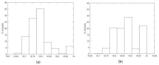
Figure 9.
Breakdown voltage distribution of A1 (a) and A3 (b).
Table 2.
Mean breakdown voltage and its standard deviation for array 1 and array 3 of three dual-layer chips.
5.2. Dark Count Rate
The “1-by-1” measurement was performed to have better insight into the DCR of every single SPAD of the array with a TIT of 30 s. A higher DCR was observed in D3 during the extended measurement compared to D1 and D2. This increase was attributed to a temperature rise, which was likely caused by the small dimensions and plastic material of D3 case, leading to insufficient heat dissipation. Unfortunately, direct temperature measurement of the chip was not possible, and the plastic case could not be removed, as it served to protect the bonding connections. To confirm that the temperature increase was indeed responsible for the observed DCR increase, the results were compared with measurements relevant to D1 and D2 conducted inside a climatic chamber at a constant temperature of 40 °C. All the chips were biased at 1.5 V excess voltage. The similarity between the cumulative DCR curves of Figure 10a strongly suggests that there is a difference of approximately 15 °C between the chips in the two carriers. To address this issue while ensuring sensor protection, alternative packaging solutions that facilitate heat dissipation are currently under investigation.
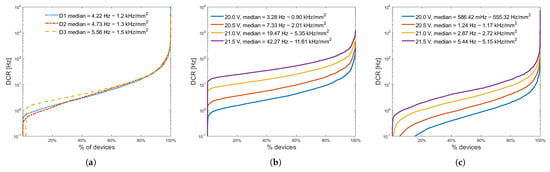
Figure 10.
DCR cumulative curves of “1-by-1” measurement for SPADs of A1 of three dual-layer chips biased at 1.5 V excess voltage (a). D1 and D2 are bonded in a CPGA144 package, while D3 is bonded in a small PCB carrier. DCR cumulative curves of “AllON” measurement for SPADs of A1 (b) and A3 (c), biased at 1.3, 1.8, 2.3, and 2.8 V excess voltage.
On the other hand, the “AllON” measurement, where all pixels are enabled simultaneously, has a much shorter duration (few minutes), making it less susceptible to temperature increase. Measurements were performed for different excess voltages with a total integration time of 1 s. Figure 10b,c illustrate the cumulative curves of SPADs in A1 and A3, respectively, biased at different voltages, specifically 20 V, 20.5 V, 21 V, and 21.5 V, corresponding to excess voltages of 1.3 V, 1.8 V, 2.3 V, and 2.8 V, respectively. The median value of the cumulative curves and their corresponding rate per area are indicated in the legend. Both arrays show an almost doubling of DCR for every 500 mV increase in bias voltage.
6. Conclusions
This paper presents the design and development of a charged particle imaging probe intended for mapping the activity of laboratory sources and radio-guided surgery applications. The core sensor is a dual-tier CMOS SPAD chip, the APIX2LF, mounted on a custom PCB carrier. An SiPM was included inside the carrier to provide an external trigger signal for measurements with a source. The probe, which was carefully designed with compactness and portability in mind, is battery operated and capable of sending data wirelessly, either via Wi-Fi or Bluetooth. The sensor was managed and interfaced with a microcontroller, and custom firmware was developed to support different types of measurements, including measurements with one SPAD enabled at a time, measurements with all SPADs enabled, and SiPM-triggered measurements. A USB connection is available as an alternative power supply option and allows battery recharging, firmware flashing, and the data transfer protocol. Data acquisition, storage, and representation are performed using MATLAB scripts, but custom software may be developed for a more user-friendly interface in the future. The chip was characterized in a dark chamber at room temperature, and the breakdown voltage was found to be approximately 18.8 V with a variation of 75 mV. The dark count rate was measured both with one SPAD enabled at a time and with all SPADs enabled for different excess voltages. At an excess voltage of 1.3 V, the median value of the DCR was less than 1 kHz/mm2. The results are consistent with other measurements conducted on the same chip samples with a purposely developed benchtop setup. Further measurements will be carried out in future work to evaluate the sensor performance with a radioactive source, and trigger measurements could offer valuable information about the APIX2LF chip potential for use in various charged particle detection applications. These measurements could also enable a comparison with other solutions described in the literature.
Author Contributions
Conceptualization, P.B., G.C., G.-F.D.B., P.S.M., J.M., F.M., L.P., L.R., G.T. and C.V.; methodology, P.B., J.M. and F.M.; software, J.M. and G.T.; validation, P.B., J.M. and F.M.; investigation, J.M.; resources, P.B., G.C., P.S.M. and F.M.; writing—original draft preparation, J.M.; writing—review and editing, P.B., G.C., G.-F.D.B., P.S.M., J.M., F.M., L.P., L.R., G.T. and C.V.; supervision, C.V. and L.R.; funding acquisition, P.S.M. All authors have read and agreed to the published version of the manuscript.
Funding
The activity leading to the results presented in this paper was carried out in the framework of the APIX2/ASAP project, funded by the Italian Institute for Nuclear Physics (INFN).
Data Availability Statement
Data relevant to the components used in the probe are publicly available on the websites of the different manufacturers. Row data relevant to the SPAD array characterization are available upon request from the corresponding author.
Conflicts of Interest
The authors declare no conflict of interest. The funders had no role in the design of the study; in the collection, analyses, or interpretation of data; in the writing of the manuscript; or in the decision to publish the results.
References
- Niclass, C.; Soga, M.; Matsubara, H.; Ogawa, M.; Kagami, M. A 0.18 μm CMOS SoC for a 100 m-Range 10 Frame/s 200 ×96-Pixel Time-of-Flight Depth Sensor. IEEE J. Solid-State Circuits 2014, 49, 315–330. [Google Scholar] [CrossRef]
- Popleteeva, M.; Haas, K.T.; Stoppa, D.; Pancheri, L.; Gasparini, L.; Kaminski, C.F.; Cassidy, L.D.; Venkitaraman, A.R.; Esposito, A. Fast and simple spectral FLIM for biochemical and medical imaging. Opt. Express 2015, 23, 23511–23525. [Google Scholar] [CrossRef] [PubMed]
- Braga, L.; Gasparini, L.; Grant, L.; Henderson, R.; Massari, N.; Perenzoni, M.; Stoppa, D.; Walker, R. A Fully Digital 8 × 16 SiPM Array for PET Applications With Per-Pixel TDCs and Real-Time Energy Output. IEEE J. Solid-State Circuits 2014, 49, 301–314. [Google Scholar] [CrossRef]
- Kostamovaara, J.; Tenhunen, J.; Kögler, M.; Nissinen, I.; Nissinen, J.; Keränen, P. Fluorescence suppression in Raman spectroscopy using a time-gated CMOS SPAD. Opt. Express 2013, 21, 31632–31645. [Google Scholar] [CrossRef] [PubMed]
- Pratte, J.F.; Nolet, F.; Parent, S.; Vachon, F.; Roy, N.; Rossignol, T.; Deslandes, K.; Dautet, H.; Fontaine, R.; Charlebois, S.A. 3D Photon-To-Digital Converter for Radiation Instrumentation: Motivation and Future Works. Sensors 2021, 21, 598. [Google Scholar] [CrossRef] [PubMed]
- Pancheri, L.; Brogi, P.; Collazuol, G.; Dalla Betta, G.F.; Ficorella, A.; Marrocchesi, P.; Morsani, F.; Ratti, L.; Savoy-Navarro, A. First prototypes of two-tier avalanche pixel sensors for particle detection. Nucl. Instrum. Methods Phys. Res. Sect. A Accel. Spectrometers Detect. Assoc. Equip. 2017, 845, 143–146. [Google Scholar] [CrossRef]
- Pancheri, L.; Ficorella, A.; Brogi, P.; Collazuol, G.; Dalla Betta, G.F.; Marrocchesi, P.; Morsani, F.; Ratti, L.; Savoy-Navarro, A.; Sulaj, A. First Demonstration of a Two-Tier Pixelated Avalanche Sensor for Charged Particle Detection. IEEE J. Electron Devices Soc. 2017, 5, 404–410. [Google Scholar] [CrossRef]
- Ratti, L.; Brogi, P.; Collazuol, G.; Dalla Betta, G.F.; Marrocchesi, P.S.; Pancheri, L.; Sulay, A.; Torilla, G.; Vacchi, C. Layered CMOS SPADs for Low Noise Detection of Charged Particles. Front. Phys. 2021, 8, 607319. [Google Scholar] [CrossRef]
- Alonso, O.; Casanova, R.; Dieguez, A.; Dingfelder, J.; Hemperek, T.; Kishishita, T.; Kleinohl, T.; Koch, M.; Krüger, H.; Lemarenko, M.; et al. DEPFET Active Pixel Detectors for a Future Linear e+e− Collider. IEEE Trans. Nucl. Sci. 2013, 60, 1457–1465. [Google Scholar] [CrossRef]
- Donnarumma, R.; Bocci, V.; Capparella, E.; Collamati, F.; Cremonesi, M.; Ferrari, M.; Fioroni, F.; Grana, C.; Ioannidis, G.; Iori, M.; et al. C.356—A novel radioguided surgery technique exploiting beta-decay. Phys. Medica 2016, 32, 104–105. [Google Scholar] [CrossRef]
- Collamati, F.; Maccora, D.; Alfieri, S.; Bocci, V.; Cartoni, A.; Collarino, A.; Simoni, M.D.; Fischetti, M.; Fratoddi, I.; Giordano, A.; et al. Radioguided surgery with β- radiation in pancreatic neuroendocrine tumors: A feasibility study. Sci. Rep. 2020, 10, 4015. [Google Scholar] [CrossRef] [PubMed]
- Marrocchesi, P.; Brogi, P.; Bigongiari, G.; Checchia, C.; Collazuol, G.; Dalla Betta, G.F.; Ficorella, A.; Lodola, L.; Morsani, F.; Musacci, M.; et al. APiX: A Geiger-mode Avalanche Digital Sensor for Particle Detection. In Proceedings of the 2017 IEEE Nuclear Science Symposium and Medical Imaging Conference (NSS/MIC), Atlanta, GA, USA, 1–28 October 2017; pp. 1–4. [Google Scholar] [CrossRef]
- Brogi, P.; Bigongiari, G.; Checchia, C.; Collazuol, G.; Dalla Betta, G.F.; Ficorella, A.; Marrocchesi, P.; Morsani, F.; Musacci, M.; Torilla, G.; et al. APiX, a two-tier avalanche pixel sensor for digital charged particle detection. Front. Phys. Nucl. Instrum. Methods Phys. Res. Sect. Accel. Spectrometers Detect. Assoc. Equip. 2020, 958, 162546. [Google Scholar] [CrossRef]
- Sulaj, A. Development of a Solid-State Imaging Probe for Radio-Guided Surgery. Ph.D. Thesis, Università degli Studi di Siena, Siena, Italy, 2021. [Google Scholar]
- Bedir, M.; Thomadsen, B.; Bednarz, B. Development and characterization of a handheld radiation detector for radio-guided surgery. Radiat. Meas. 2020, 135, 106362. [Google Scholar] [CrossRef]
- Massari, R.; Ucci, A.; Campisi, C.; Scopinaro, F.; Soluri, A. A novel fully integrated handheld gamma camera. Nucl. Instruments Methods Phys. Res. Sect. Accel. Spectrometers Detect. Assoc. Equip. 2016, 832, 271–278. [Google Scholar] [CrossRef]
- Dinu, N.; Imando, T.A.; Nagai, A.; Pinot, L.; Puill, V.; Callier, S.; Janvier, B.; Esnault, C.; Verdier, M.A.; Raux, L.; et al. SiPM arrays and miniaturized readout electronics for compact gamma camera. Nucl. Instruments Methods Phys. Res. Sect. Accel. Spectrometers Detect. Assoc. Equip. 2015, 787, 367–372. [Google Scholar] [CrossRef]
- Russomando, A.; Bellini, F.; Bocci, V.; Collamati, F.; De Lucia, E.; Faccini, R.; Marafini, M.; Mattei, I.; Chiodi, G.; Patera, V.; et al. An Intraoperative β− Detecting Probe for Radio-Guided Surgery in Tumour Resection. IEEE Trans. Nucl. Sci. 2016, 63, 2533–2539. [Google Scholar] [CrossRef]
- Espressif. ESP32-WROVER Datasheet. 2017. v2.6. Available online: https://www.espressif.com/sites/default/files/documentation/esp32_technical_reference_manual_en.pdf (accessed on 1 February 2023).
- ESP-IDF Programming Guide. Available online: https://docs.espressif.com/projects/esp-idf/en/release-v4.1/ (accessed on 7 February 2023).
- Gray, F.; Smith, M. SECONDARY BATTERIES–LITHIUM RECHARGEABLE SYSTEMS | Lithium Polymer Batteries. In Encyclopedia of Electrochemical Power Sources; Garche, J., Ed.; Elsevier: Amsterdam, The Netherlands, 2009; pp. 169–176. [Google Scholar] [CrossRef]
- RS PRO, 3.7 V, 19 (Dia.) x69 mm, Lithium-Ion Rechargeable Battery, 2.6 Ah. Available online: https://docs.rs-online.com/d431/A700000008874156.pdf (accessed on 8 February 2023).
- Torilla, G. Characterization of 150 nm CMOS SPAD Arrays for a Dual Layer Position Sensitive Detector. Master’s Thesis, Università degli Studi di Pavia, Pavia, Italy, 2020. [Google Scholar]
- Ratti, L.; Brogi, P.; Collazuol, G.; Dalla Betta, G.F.; Marrocchesi, P.; Minga, J.; Morsani, F.; Pancheri, L.; Torilla, G.; Vacchi, C. Cross-talk and RTS Noise Characterization of 1- and 2-tier CMOS SPADs in a 150 nm Process. In Proceedings of the 2021 IEEE Nuclear Science Symposium and Medical Imaging Conference (NSS/MIC), Online, 16–23 October 2021; pp. 1–4. [Google Scholar] [CrossRef]
- Torilla, G.; Minga, J.; Brogi, P.; Collazuol, G.; Dalla Betta, G.F.; Marrocchesi, P.S.; Pancheri, L.; Ratti, L.; Vacchi, C. DCR and crosstalk characterization of a bi-layered 24 × 72 CMOS SPAD array for charged particle detection. Nucl. Instrum. Meth. A 2023, 1046, 167693. [Google Scholar] [CrossRef]
- Texas Instruments. TPS6104x Low-Power DC-DC Boost Converter in SOT-23 and WSON Packages Ddatasheet. Rev. K. 2002. Available online: https://www.ti.com/lit/gpn/tps61041 (accessed on 1 February 2023).
- Pancheri, L.; Dalla Betta, G.F.; Braga, L.H.C.; Xu, H.; Stoppa, D. A single-photon avalanche diode test chip in 150 nm CMOS technology. In Proceedings of the 2014 International Conference on Microelectronic Test Structures (ICMTS), Udine, Italy, 24–27 March 2014; pp. 161–164. [Google Scholar]
- Donahoo, M.J.; Calvert, K.L. TCP/IP Sockets in C: Practical Guide for Programmers, 2nd ed.; The Morgan Kaufmann Practical Guides Series; Morgan Kaufmann: Amsterdam, The Netherlands, 2009. [Google Scholar]
- BLE User Guide. Available online: https://mynewt.apache.org/latest/network/ (accessed on 16 February 2023).
- Fishburn, M.W.; Maruyama, Y.; Charbon, E. Reduction of Fixed-Position Noise in Position-Sensitive Single-Photon Avalanche Diodes. IEEE Trans. Electron. Devices 2011, 58, 2354–2361. [Google Scholar] [CrossRef]


Disclaimer/Publisher’s Note: The statements, opinions and data contained in all publications are solely those of the individual author(s) and contributor(s) and not of MDPI and/or the editor(s). MDPI and/or the editor(s) disclaim responsibility for any injury to people or property resulting from any ideas, methods, instructions or products referred to in the content. |
© 2023 by the authors. Licensee MDPI, Basel, Switzerland. This article is an open access article distributed under the terms and conditions of the Creative Commons Attribution (CC BY) license (https://creativecommons.org/licenses/by/4.0/).