
Analysis and Design of the High Current Rising Rate Hybrid DC Current Limiting Circuit Breaker
by
Zhiyong Lv
1,
Xiangjun Wang
1,
Jinwu Zhuang
1,
Luhui Liu
2,
Zhifang Yuan
2,
Siguang Li
1 and
Jin Wu
1,* 1
College of Electrical Engineering, Naval University of Engineering, Wuhan 430030, China
2
National Key Laboratory of Science and Technology on Vessel Integrated Power System, Naval University of Engineering, Wuhan 430030, China
*
Author to whom correspondence should be addressed.
Electronics 2023, 12(12), 2657; https://doi.org/10.3390/electronics12122657
Submission received: 17 May 2023
/
Revised: 8 June 2023
/
Accepted: 10 June 2023
/
Published: 13 June 2023
(This article belongs to the Topic Power System Protection)
(This article belongs to the Section Power Electronics)
(This article belongs to the Section Power Electronics)
Abstract
:To solve the problem of the high rising rate and large peak value of the expected current of the short-circuit current in marine DC power system faults, a hybrid DC current limiting circuit breaker scheme based on a high-speed electromagnetic repulsion mechanism is proposed. A parameter selection model is constructed by comprehensively considering the short-time withstand of the thyristor, the volume of the commutation circuit, and capacitor energy, and the optimal value of the commutation circuit parameters at a certain voltage level is obtained. The finite element mathematical model of the high-speed electromagnetic repulsion mechanism is established by coupling the electromagnetic force field, which enables the deformation process of the mechanism under the condition of high acceleration to be considered. The von Mises yield criterion is adopted as the mechanical boundary condition in the design of a high-speed electromagnetic repulsion mechanism, which solves the problem of the long inherent time of opening. The experiment platform is built, and the experiment under the fault condition with a current rising rate of 20 A/μs is completed. The arcing time, commutation time, zero-voltage recovery time, and contact movement characteristics are obtained, which meet the design requirements, verify the effectiveness of the analysis, and lay a solid foundation for further research and development of the current limiting circuit breakers for medium voltage DC systems.
1. Introduction
With the improvement of ship electrification and the emergence of high-energy weapons, the capacity level of ship power systems is increasing, and the rising rate of the short-circuit current can reach 20 A/μs. This puts forward high requirements for the rapidity of the protection device of ship power systems [1,2,3].
The action time of traditional mechanical circuit breakers is generally milliseconds [4], which causes difficulty in meeting the existing requirements. Solid-state circuit breakers have the disadvantage of a large rated current loss and need additional heat dissipation devices [5,6,7]. With the development of DC breaking technology, many new technologies have appeared in recent years [8,9,10,11,12,13,14,15,16].
Reference [8] proposes a novel medium voltage DC (MVDC) commutation-breaking topology that combines a load-carrying branch and an arcing branch in parallel. In contrast to the conventional structure based on semiconductor devices, each branch in the proposed topology contains a mechanical contact, which provides a lower on-state loss and higher voltage-breaking capacity. Moreover, the theoretical analysis and experimental results verified the asynchronous operation of the current loading and confirmed that the arcing branch could realize the natural commutation of the current for the breaking of overload current or short-circuit current. Since the structure adopts the method of natural commutation, the commutation speed will not be too high to meet the requirements of the high rising rate.
Reference [9] deals with a principle of AC/DC interruption for low-voltage air circuit breakers. When a fault occurs, by squeezing the arc into constricted insulating slits, the arc resistance is elevated, resulting in an arc voltage that is higher than the system voltage. Hence, the fault current would decrease until the arc plasma cannot be maintained. This method can quickly establish a higher voltage than the conventional air arc, but at the same time, the cooperation of the driving mechanism is more complex, which increases the difficulty of the design.
Reference [10] proposes a new hybrid DC circuit breaker utilizing a series-connected coupled inductor connected, which enables automatic current commutation from the mechanical switch to the semiconductor switch during a fault. The key advantage of the proposed DC circuit breaker is that the current in the mechanical switch automatically reduces to zero when a fault happens. Although this method can realize the automatic commutation of current, the inductance volume is also large when the rated current is large. At the same time, the commutation speed is slower than the forced commutation method, which does not meet the requirements of a high current rising rate.
Reference [11] proposes a new design of a DC hybrid circuit breaker based on a high-speed switch (HSS) and arc generator (AG), which can drastically profit from low heat loss in a normal state and fast current breaking under a fault state. The AG is designed according to the magnetic pinch effect of liquid metal. The fault current is rapidly commutated from HSS into the parallel connected branch by utilizing the arc voltage generated across the AG. As a consequence, the arcless open of HSS is achieved. The fluidity of the liquid will become worse after the breaker is used many times, which may be due to the reaction between liquid metal and air, and the flow rate of this method is smaller than that of the forced commutation method.
The hybrid DC current-limiting circuit breaker (HDCCLCB) combines the advantages of the large capacity of the mechanical switch and the rapidity of the solid-state switch, which becomes the development direction for solving the problem of fast DC breaking [12,13,14,15,16]. In this paper, a hybrid vacuum current limiting circuit breaker based on a high-speed electromagnetic repulsion mechanism (ERM) is proposed, which uses the excellent arc extinguishing ability of the vacuum interrupter and the rapidity of the ERM to complete the fault breaking of the system short-circuit current.
2. Principle of the HDCCLCB Based on the Electromagnetic Repulsive Vacuum Switch
The circuit topology of the HDCCLCB is shown in Figure 1. The HDCCLCB is mainly composed of the high-speed vacuum interrupter VI, power electronic commutation circuit, metal oxide varistor (MOV), and reverse parallel diode D. Its working process is as follows:
(1) In the normal working condition, the main circuit current i0 flows through the vacuum interrupter VI;
(2) When the current needs to be cut off, the vacuum interrupter VI is opened, and the vacuum arc appears;
(3) After a short arcing time, the thyristor T of the commutation circuit is triggered, and the pre-charged capacitor C discharges the vacuum interrupter VI through the inductor L; the reverse parallel diode D cannot be turned on due to the clamping effect of the arc voltage, so all the pulse current flow to the VI. The pulse current i is opposite to the main circuit current, which makes the current iVI gradually decrease until the current zero crossing is formed;
(4) Because the reverse pulse current flows through the reverse parallel diode D after the arc is extinguished, the voltage drop on the contact of the VI is approximately zero. The transient recovery overvoltage will not occur until the pulse current is equal to the main circuit current again. During this phase, the VI achieves the zero-voltage recovery time. In this process, the vacuum interrupter contact is still in movement, and the contact opening distance increases continuously, which is more conducive to the successful breaking of the VI.
3. Analysis and Design of the Commutation Process and Commutation Parameters
3.1. Equivalent Circuit of the Commutation Process
Figure 2 shows the typical waveform of the current and voltage during the operation of the circuit breaker. According to the working principle of the circuit breaker, the equivalent circuit analysis is carried out for each phase of the operation.
In Figure 2, for : at 0, the short-circuit fault occurs in the system; at , when the current reaches the circuit breaker protection setting value , the VI is triggered; after the inherent time () of the VI, the movable contact opens at t2. At this phase, all the short-circuit current flows through the mechanical contact of the VI, and the VI is in a closing state. The circuit breaker can be equivalent to the resistance and inductance of the VI branch in series. The equivalent circuit diagram is shown in Figure 3. The thyristor conduction voltage drop is ignored in the equivalent circuit.
For : at t2, the VI contact opens, and there is an arc between the contacts; the arc voltage is ; at t3, the commutation circuit is turned on; the contact arcing time () is defined. The equivalent circuit diagram of this phase is shown in Figure 4.
For : at t3, the commutation circuit is turned on to generate pulse current; due to the clamping effect of the arc voltage of the VI, the reverse parallel diode D is not turned on; with the increase in the pulse current, the current of the VI decreases gradually; at t4, the current of the VI drops to zero, the current is completely commutated to the commutation circuit, and the commutation time is (). The equivalent circuit at this phase is shown in Figure 5, where C is the commutation capacitor, U is the pre-charge voltage, R is the resistance, and L is the inductance of the commutation circuit.
For : at t4, the current of the VI decreases to zero, the vacuum arc is extinguished, and the reverse parallel diode D starts to be turned on; as the current of the commutation circuit continues to increase, the current of the commutation circuit commutates to diode D; until the current of the commutation circuit drops to the current of the main circuit again, the reverse parallel diode D is cut off, and recovery voltage starts to appear at two ends of the VI. The conduction time of the diode is the recovery time () of zero voltage after arcing of the VI. The equivalent circuit diagram of this phase is shown in Figure 6.
3.2. Design of the Commutation Circuit Parameters
The design of the commutation circuit parameters mainly involves the phase. The phase determines the arcing time tr before commutation, which, together with the following phase, determines the arcing energy Q of the contact. The phase determines the zero-voltage time tL of the contact. According to the working principle of the circuit breaker, the parameter design of the commutation circuit shall meet the following conditions:
(1) The peak value of the commutation circuit current I6 shall be greater than the corresponding main circuit current Imax;
(2) In order to meet the need for dielectric recovery of the VI, zero-voltage time ;
(3) The current of the commutation circuit shall flow through the VI to reduce the energy stored in the capacitor;
(4) Due to the limitation of the short-time withstand of the thyristor, the initial rising rate of current in the commutation circuit .
When ignoring the resistance R of the commutation circuit, the resistance of the VI, the inductance of the VI, the conduction voltage drop of the diode, and the arc voltage, the commutation circuit can be simplified as a second-order circuit in the zero state. The current-limiting resistance R is small, which can be ignored. To further simplify the problem, assume that the cycle T of the second-order circuit is a constant k multiple of the zero-voltage time tL, that is, . The following equation can be obtained:
Ignoring the resistance of the commutation circuit R and the resistance of the vacuum switch RVI, the equivalent circuit diagram of the commutation process is shown in Figure 7, where i is the current of the commutation circuit, iD is the current of the reverse parallel diode branch, and if is the reverse current flowing to the VI.
List circuit equations:
It can be obtained that the ratio of the current change rate of the current flowing to the VI and the reverse parallel diode circuit is:
Whether the diode is turned on depends on the ratio of the current change rate. When the ratio of the current change rate is less than or equal to zero, the reverse parallel diode is not turned on; that is:
Thus,
When the moment of is equal to zero, namely , the constraint condition of the initial current rising rate di/dt of the commutation circuit can be obtained:
The inductance value of the VI LVI is 0.08 μH, the diode conduction voltage drop UD is 1.8 V, and the arc voltage Uarc is 20 V, then
Because the short-time withstand of the thyristor in the commutation circuit requires that the initial current rising rate of 220 A/μs, which is less than 272 A/μs, meeting the condition that all the commutation current flows through the VI, the initial current rising rate of the commutation circuit should be less than 220 A/μs.
To sum up, each parameter needs to meet Equation (10). The capacitor charging voltage U is the system voltage 900 V, the current of the main circuit at the peak current of the commutation circuit is 15 kA, and the coefficient k is taken as five times. The parameter matching range is calculated by drawing, and the results are shown in Figure 8 and Figure 9.
Point 1 is the intersection of curves 2 and 3. Point 2 is the intersection of curves 1 and 3. The horizontal ordinations of the two points are inductance L1 and L2, respectively.
(1) When L1 is equal to L2, that is ;
(2) When , that is , L1 > L2;
The objective function is to minimize the volume of the commutation circuit. It is assumed that the larger the capacitance value is, the larger the capacitance volume is when the capacitance voltage is determined. At the same time, it is considered that the volume of current-limiting inductance is incomparable with that of capacitance. The optimal parameter combination is the parameter combination corresponding to point 1 in Figure 8, and the results are as follows:
(3) When , that is , L1 < L2.
The optimal parameter combination is the parameter combination corresponding to point 2 in Figure 9, and the results are as follows.
Under the assumption that the cycle of the commutation circuit is k times the zero-voltage time and the optimization objective is to minimize the volume of the commutation circuit, the following conclusions are obtained:
(1) When , the combination of optimal parameters are: current-limiting inductance and commutation capacitance . Each parameter is independent of the initial current rising rate of the commutation circuit and proportional to the zero-voltage time.
(2) When , the combination of optimal parameters is: current-limiting inductance and commutation capacitance . Each parameter is independent of the zero-voltage time and inversely proportional to the initial current rising rate of the commutation circuit.
Under the condition that the diode does not conduct during the commutation process, taking into account factors such as the short-time withstand of the thyristor and volume of the commutation circuit, the capacitance of 2.0 mF, pre-charge voltage of 900 V, and current-limiting inductance of 7.5 μH are selected as the parameters.
4. Analysis and Design of the High-Speed Electromagnetic Repulsion Vacuum Contact
To ensure the reliable closing of the circuit breaker, the contact opening distance shall be large enough before the end of the zero-voltage time. The ERM has become the first choice of the driving mechanism because of its advantages of the short inherent time and large initial speed. Under the condition of ensuring that the ERM will not be damaged and the requirements of the small energy consumption and small overall volume of the mechanism are met at the same time, the movable contact displacement should be maximum at 500 μs.
4.1. Geometric Model and Working Principle of the High-Speed Electromagnetic Repulsion Vacuum Contact
Figure 10a shows the geometric structure of the high-speed electromagnetic repulsion vacuum contact, which is mainly composed of the repulsion disc, the repulsion coil, and the movable and fixed contact of the vacuum interrupter.
When the ERM is working, the repulsion coil is connected with a changing current, and the changing current induces a current in the repulsion disc. The electromagnetic force between them is used to push the repulsion disc upward, so as to achieve a high speed. Figure 10b shows the drive circuit of the repulsion coil. The diode is reversely connected in parallel at two ends of the repulsion coil using the capacitor discharge to generate the changing current to prevent the current reverse and improve the efficiency of the capacitor current.
4.2. Mathematical Model of the High-Speed Electromagnetic Repulsion Vacuum Contact
Different from the applications of the traditional vacuum contact, in order to limit the short-circuit current quickly, the vacuum contact needs to obtain a higher initial speed, which requires that the repulsion disc is able to withstand huge stress and that it is not damaged. Once the repulsive disc has a large elastic deformation, the inherent time of the vacuum contact will become larger. Considering the possible deformation under high acceleration, dynamic simulation analysis must be carried out. The finite element mathematical model is established by combining the electromagnetic force fields.
To numerically solve the kinematic characteristics of the high-speed electromagnetic repulsion mechanism based on COMSOL Multiphysics finite element calculation software, the external circuit interface, electromagnetic field interface, global differential interface, algebraic equation interface, event interface, and dynamic grid interface are required. The external circuit interface simulates the capacitor discharge and provides the excitation current to the repulsive coil; by using the electromagnetic field interface, the current density, magnetic induction intensity, and electromagnetic force in the region are solved. The electromagnetic force on the repulsive disc is obtained by integrating the Lorentz force; through the global differential interface, algebraic equation interface, event interface, and dynamic grid interface, combined with the mass of moving parts, the electromagnetic force and spring pressure of the mechanism, the motion equation of the electromagnetic repulsion mechanism can be listed. The mathematical model is as follows:
Electromagnetic field equation:
where H is the magnetic field strength, in A/m, B is the magnetic induction vector, in T; J is the current density vector, in A/m2; A is the magnetic vector, in Wb/m; E is the electric field intensity vector, in V/m; is the magnetic permeability, in H/m; is the conductivity, in S/m.
Lorentz force and electromagnetic force in a repulsive disc:
where F is the Lorentz force density vector, in N/m3; Fm is the electromagnetic force obtained by integrating Lorentz forces.
The mechanical movement equation is as follows:
where Fm is the electromagnetic force on the repulsive disc; Fs is the force exerted by others, including the spring force and gravity of moving parts; m is the mass of moving parts such as the repulsive disc, shaft, and moving contact; and z is the axial displacement of repulsive disc.
During the motion of the repulsive disc, due to the action of the non-uniform Lorentz force, when the equivalent stress of the repulsive disc does not exceed its yield strength, there will be elastic deformation accompanying the repulsive disc. Load the Lorentz force onto the repulsive disc, apply a fixed constraint on the inner diameter of the repulsive disc, and track its vertical displacement through the motion equation coupled the dynamic grid. Linear elasticity problems are solved mainly through the equilibrium equation, stress-strain relationship, and deformation continuity equation. The tensor expression of the three groups of equations is as follows:
where ρ represents the material density; u represents the displacement vector of a particle in a repulsive disc; Fv represents the force acting on the particles in the disc; σ is the Cauchy stress tensor; is the extremely micro strain tensor; C represents the fourth order stiffness tensor; represents the inner product of two second-order tensors. In the finite element solution of the repulsion mechanism, the structural mechanics module is coupled to obtain the stress, strain, and displacement of the repulsion disc.
4.3. The von Mises Yield Criterion
The repulsive disc is usually made of plastic materials such as copper, aluminum, and steel. Under the action of external forces within a certain range, these materials can return to their original shape after the stress unloading, even if significant elastic deformation occurs. Whether the plastic material undergoes elastic deformation is generally determined by the theory of distortion energy. When the distortion energy of the material exceeds its limit value, it will yield and produce plastic deformation. This criterion can also be determined by the von Mises yield criterion shown in Equation (18); that is, when the von Mises equivalent stress of the material exceeds its yield strength, the deformation changes from elastic deformation to plastic deformation. In this paper, the criterion is used as the boundary condition of mechanism mechanics.
where is the von Mises equivalent stress; , and are the first, second, and third principal stresses, respectively; and is the yield strength, in Pa.
4.4. Optimization Design of the High-Speed ERM
The simulation model of the high-speed ERM is established, as shown in Figure 11, and the structural parameters are shown in Table 1.
Considering that the repulsive disc needs to have good conductivity and high structural strength, it was screened among several commonly used materials. The material properties are shown in Table 2. As shown in Figure 12, the contact displacement curves of the repulsive disc with different materials are, respectively, shown. It can be seen from Figure 12 that the contact displacement of copper, beryllium bronze, and T300 steel decreased gradually. The main reason is that the displacement is due to the different conductivity of materials; the greater the conductivity is, the greater the induced current in the repulsion disc is, the greater the electromagnetic repulsion force is, and the greater the displacement is.
Figure 13 shows the distribution diagram of the equivalent stress with different materials. The maximum stresses of the repulsive disc of the copper, beryllium bronze, and T300 steel are 900 MPa, 1000 Mpa, and 1600 MPa, respectively; the yield strength distributions of the three are 70 MPa, 1035 Mpa, and 1957 MPa, respectively. The yield strength requirements can only be met when beryllium bronze and T300 steel are used. Finally, beryllium bronze is selected as the material of the repulsion disc, which can ensure that the maximum equivalent stress is less than the yield strength and the displacement is larger.
5. Prototype Experiment
The prototype is manufactured and the experiment platform is built. As shown in Figure 14, the platform structure diagram is shown, and Figure 15 is the experiment site.
The following is an introduction to the short-circuit breaking capacity experiment process of the HDCCLCB.
(1) At zero time, the thyristor TH0 is triggered to generate a fault current. The fault current with different rising rates can be obtained by adjusting the inductance L0.
(2) When the current of the high-speed mechanical switch reaches the set value, the driving circuit of the mechanical switch is triggered and simultaneously triggers the high-speed camera to start shooting.
(3) When the switch is opened, the thyristor TH1 is triggered after a delay time.
(4) In the experiment, the current and voltage information is obtained by the Rogowski coil and high-voltage probe, respectively. The high-speed camera is used to capture the contact movement image. The displacement curve can be obtained after post-processing. Figure 16 shows the experimental and simulation displacement curves of the contact. The typical working process waveform is shown in Figure 17.
Figure 16 shows the experimental and simulation displacement curves of the contact. It can be seen from Figure 16 that the error of the contact displacement curve between the experiment and simulation curves is small, and the average movement speed within 1 ms of the contact is 2 m/s.
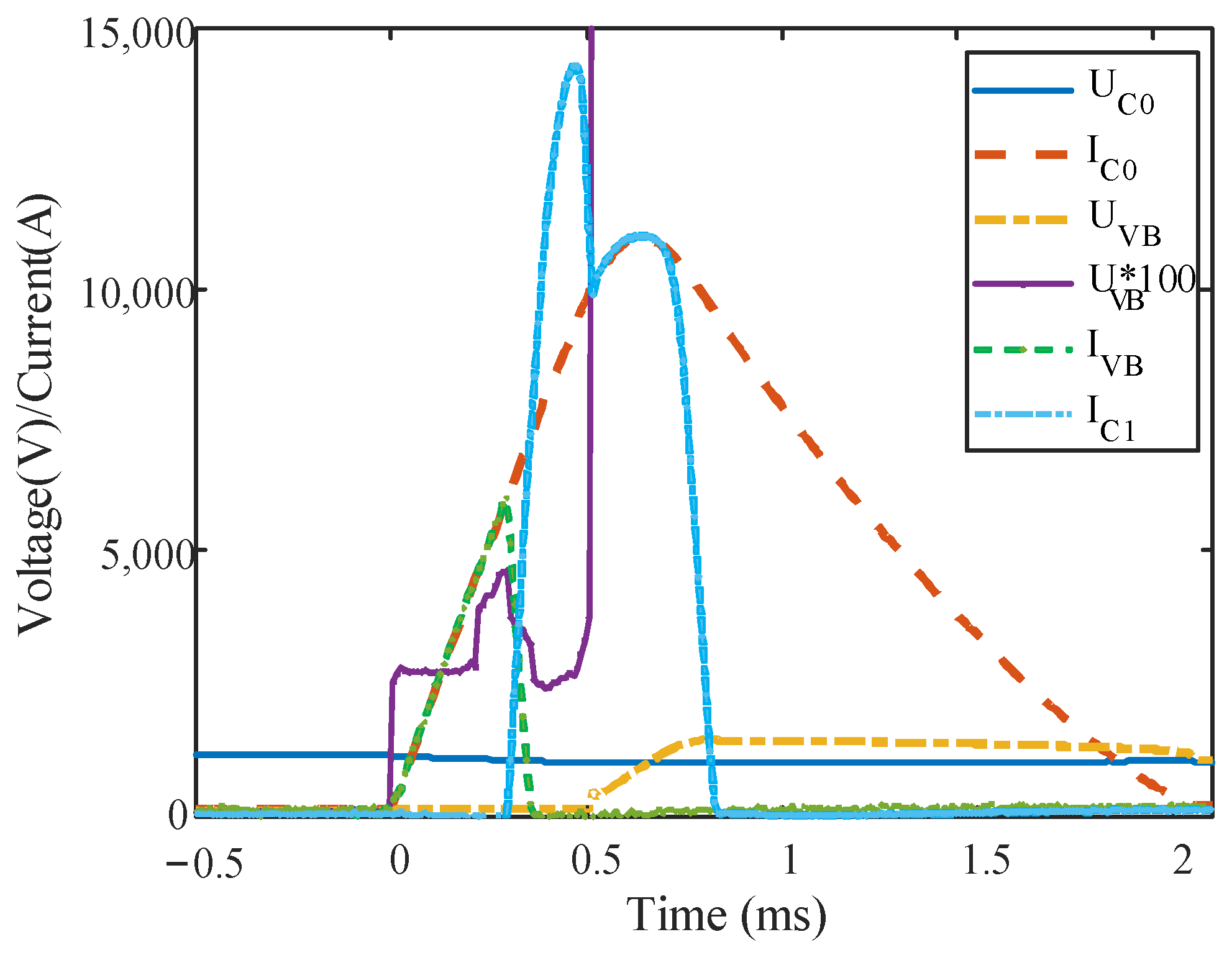
As shown in Figure 17, the voltage of the experiment system is 1 kV, and the rising rate of the short-circuit current is 20 A/μs. The waveforms of the main circuit current/voltage, contact current/voltage, and commutation circuit current are recorded, respectively. At zero time, the system is short-circuited, and the current rising rate is 20 A/μs; at 100 μs, the thyristor of the ERM is triggered; at 220 μs, after the mechanism inherent time 120 μs, the vacuum contact opens and generates the vacuum arc; at 290 μs, after the arcing time 70 μs, the commutation circuit starts to work, and the main circuit current drop rate is 109 A/μs; at 350 μs, after the commutation time 60 μs, the commutation ends; at 500 μs, after the zero-voltage time 150 μs, two ends of the contact appear at the transient voltage 450 V, and then the voltage firstly rises and then falls back to be consistent with the system voltage. Table 3 shows the time sequence of the breaking process.
6. Discussion
On the basis of the traditional topology, the new HDCCLCB can provide a zero-voltage recovery time after the contact current crosses zero by reverse paralleling diodes at two ends of the VI. Traditional topology structures require a large opening distance of the VI to perform commutation, which requires a certain amount of time. When the rising rate of the short-circuit current is high, it can cause the short-circuit current to become large. At the same time, the larger short-circuit current requires a larger opening distance to enable the contact to withstand transient overvoltage after the current crosses zero. The zero-voltage recovery time of the new topology structure reduces the requirement for the contact opening distance, allowing the VI to withstand the transient overvoltage within a small opening distance. Therefore, we can preliminarily conclude that the new HDCCLCB is more suitable for situations with high short-circuit current rising rates and is more suitable for short-circuit protection in ship DC systems.
At the same time, a new problem arises, which is that in short-distance situations, the arc is an intense vacuum arc. This type of vacuum arc has a higher plasma density, greater pressure, and is more prone to post-arc breakdown compared to diffused vacuum arc with larger open distances. Therefore, it is crucial to design a zero-voltage time so that this intense vacuum arc can be fully restored in the post-arc stage. Indeed, there are not even analytical concepts to handle it. It seems a worthwhile phenomenon for further systematic experimental and theoretical studies under more refined conditions. The next step will focus on modeling and analyzing the post-arc recovery process of intense vacuum arcs, completing the post-arc dielectric recovery theory to better guide the design of current limiting circuit breakers.
The developed prototype is rated for a maximum di/dt ~ 20 A/μs with an interruptible current of about 10 kA, but the obtained results can be considered valid also for higher current and voltage values, provided that a higher number of VI is connected in parallel and series. The new HDCCLCB will be suitable for the protection field of ship DC power systems with higher voltage and current levels.
7. Conclusions
To solve the problem that existing circuit breakers cannot protect the DC power system quickly when the high rising rate short-circuit current fault occurs, an HDCCLCB scheme based on high-speed mechanical switches and power electronic devices is proposed in this paper. The parameters of the commutation circuit and the mechanical boundary conditions of the high-speed mechanical switch are analyzed and calculated, and the following conclusions are drawn:
(1) The proposed parameter selection model can comprehensively consider the short-time withstand of the thyristor, volume of the commutation circuit, and capacitor energy, which can quickly obtain the combination of optimal parameters at a certain voltage level.
(2) The finite element mathematical model of the high-speed electromagnetic repulsion mechanism established by coupling the electromagnetic force field can consider the stress distribution during the working process.
(3) Adopting the von Mises yield criterion as the mechanical boundary condition in the design of a high-speed electromagnetic repulsion mechanism can ensure that the stress of the mechanism is within a reasonable range, improve the service life of the mechanism, and solve the problem of the long inherent time of opening.
(4) When the vacuum gap is 0.74 mm and the short-circuit current is within the current range of 4500~6000 A increasing at a rate of 20 A/μs, the vacuum contact can withstand at least 450 V transient overvoltage after a 70 μs arcing time, 60 μs commutation time and 150 μs zero-voltage recovery time.
Author Contributions
Conceptualization, Z.L., X.W., J.Z. and J.W.; methodology, Z.L.; software, Z.L.; investigation, L.L. and Z.Y.; writing—original draft preparation, Z.L.; writing—review and editing, Z.L.; project administration, S.L.; funding acquisition, L.L. and Z.Y. All authors have read and agreed to the published version of the manuscript.
Funding
This research was funded by [National Natural Science Foundation of China] grant number [52107136, 51607184].
Institutional Review Board Statement
Do not require ethical approval.
Informed Consent Statement
Not involve humans.
Data Availability Statement
Data available on request from the authors.
Conflicts of Interest
The authors declare no conflict of interest.
References
- Zohrabi, N.; Shi, J.; Abdelwahed, S. An overview of design specifications and requirements for the MVDC shipboard power system. Int. J. Electr. Power Energy Syst. 2019, 104, 680–693. [Google Scholar] [CrossRef]
- Satpathi, K.; Ukil, A.; Pou, J. Short-circuit fault management in DC electric ship propulsion system: Protection requirements, review of existing technologies and future research trends. IEEE Trans. Transp. Electrif. 2018, 4, 272–291. [Google Scholar] [CrossRef]
- Fu, L.; Liu, L.; Wang, G.; Ma, F.; Ye, Z.; Ji, F.; Liu, L. The research progress of the medium voltage DC integrated power system in China. Chin. J. Ship Res. 2016, 11, 72–79. (In Chinese) [Google Scholar]
- Desbaillet, M. DC High Speed Circuit-Breaker UR6 Instructions Manual Document Number: HSBA601103TEN; Secheron SA: Geneva, Switzerland, 2008. [Google Scholar]
- Xu, Z.; Zhang, B.; Sirisukprasert, S.; Zhou, X.; Huang, A.Q. The emitter turn-off thyristor based DC circuit breaker. In Proceedings of the Power Engineering Society Winter Meeting, New York, NY, USA, 27–31 January 2002; Volume 1, pp. 288–293. [Google Scholar]
- Agostini, F.; Vemulapati, U.; Torresin, D.; Arnold, M.; Rahimo, M.; Antoniazzi, A.; Raciti, L.; Pessina, D.; Suryanarayana, H. 1MW bidirectional DC solid state circuit breaker based on air cooled reverse blocking-IGCT. In Proceedings of the 2015 Electric Ship Technologies Symposium, Alexandria, VA, USA, 21–24 June 2015; pp. 287–292. [Google Scholar]
- Kempkes, M.; Roth, I.; Gaudreau, M. Solid-state circuit breakers for medium voltage DC power. In Proceedings of the 2011 Electric Ship Technologies Symposium, Alexandria, VA, USA, 10–13 April 2011; pp. 254–257. [Google Scholar]
- Jia, B.; Wu, J.; Xia, S.; Luo, X.; Ma, S.; Jiang, Y. Analysis and Experimental Research on a Novel Multi-Contact MVDC Natural Current Commutation Breaking Topology. IEEE Access. 2020, 8, 186540–186550. [Google Scholar] [CrossRef]
- Huo, T.; Niu, C.; He, H.; Wu, Y.; Rong, M.; Zhu, M.; Zhu, X. An Arc Squeeze Method for DC Interruption Experiments and Analysis. IEEE Trans. Power Deliv. 2019, 34, 1069–1078. [Google Scholar] [CrossRef]
- Pei, X.; Smith, A.; Cwikowski, O.; Barnes, M. Hybrid DC circuit breaker with coupled inductor for automatic current commutation. Int. J. Electr. Power Energy Syst. 2020, 120, 106004. [Google Scholar] [CrossRef]
- Wu, Y.; Rong, M.; Wu, Y.; Yang, F.; Li, M.; Zhong, J.; Han, G.; Niu, C.; Hu, Y. Investigation of DC hybrid circuit breaker based on highspeed switch and arc generator. Rev. Sci. Instrum. 2015, 85, 024704. [Google Scholar] [CrossRef] [PubMed]
- Shukla, A.; Demetriades, D. A survey on hybrid circuit breaker topologies. IEEE Trans. Power Deliv. 2015, 30, 627–641. [Google Scholar] [CrossRef]
- Polman, H.; Ferreira, J.A.; Kaanders, M.; Evenblij, B.H.; Van Gelder, P. Design of a bi-directional 600V/6kA ZVS hybrid DC switch using IGBTs. IEEE Trans. Power Deliv. 2001, 16, 1052–1059. [Google Scholar]
- Meyer, J.; Rufer, A. A DC hybrid circuit breaker with ultra-fast contact opening and integrated gate-commutated thyristors (IGCTs). IEEE Trans. Power Deliv. 2006, 21, 646–651. [Google Scholar] [CrossRef]
- Häfner, J.; Jacobson, B. Proactive hybrid HVDC breakers-a key innovation for reliable HVDC grids. In Proceedings of the International Symposium on Integrating Supergrids and Microgrids, CIGRE, Bologna, Italy, 13–15 September 2011; pp. 1–8. [Google Scholar]
- Grieshaber, W.; Violleau, L. Development and test of a 120 kV direct current circuit breaker. In CIGRE Session; CIGRE: Paris, France, 2014; p. B4-301. [Google Scholar]
Figure 1.
The circuit topology of the HDCCLCB.

Figure 2.
Typical waveform of the HDCCLCB.
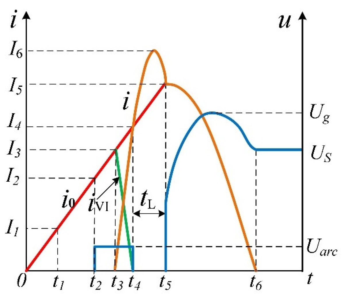
Figure 3.
Equivalent circuit of the 0→t2 phase.
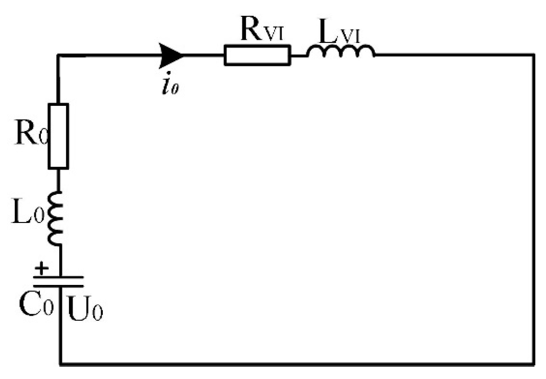
Figure 4.
Equivalent circuit of the t2→t3 phase.

Figure 5.
Equivalent circuit of the t3→t4 phase.

Figure 6.
Equivalent circuit of the t4→t5 phase.
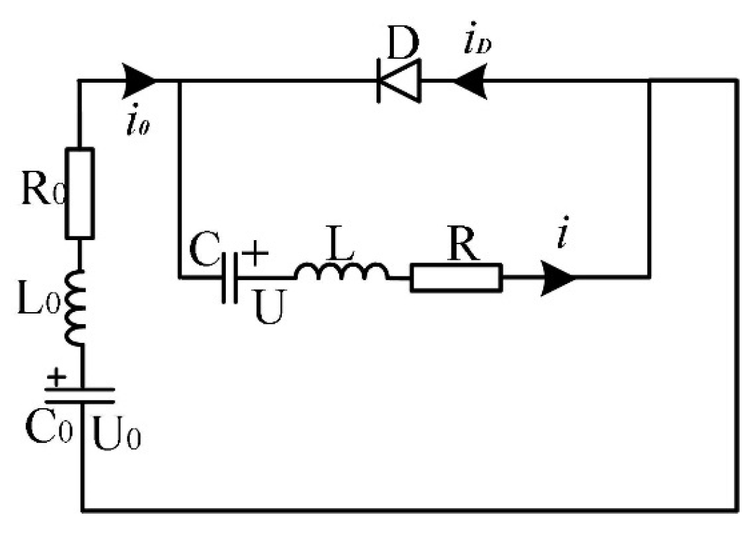
Figure 7.
Equivalent circuit of the commutation process.
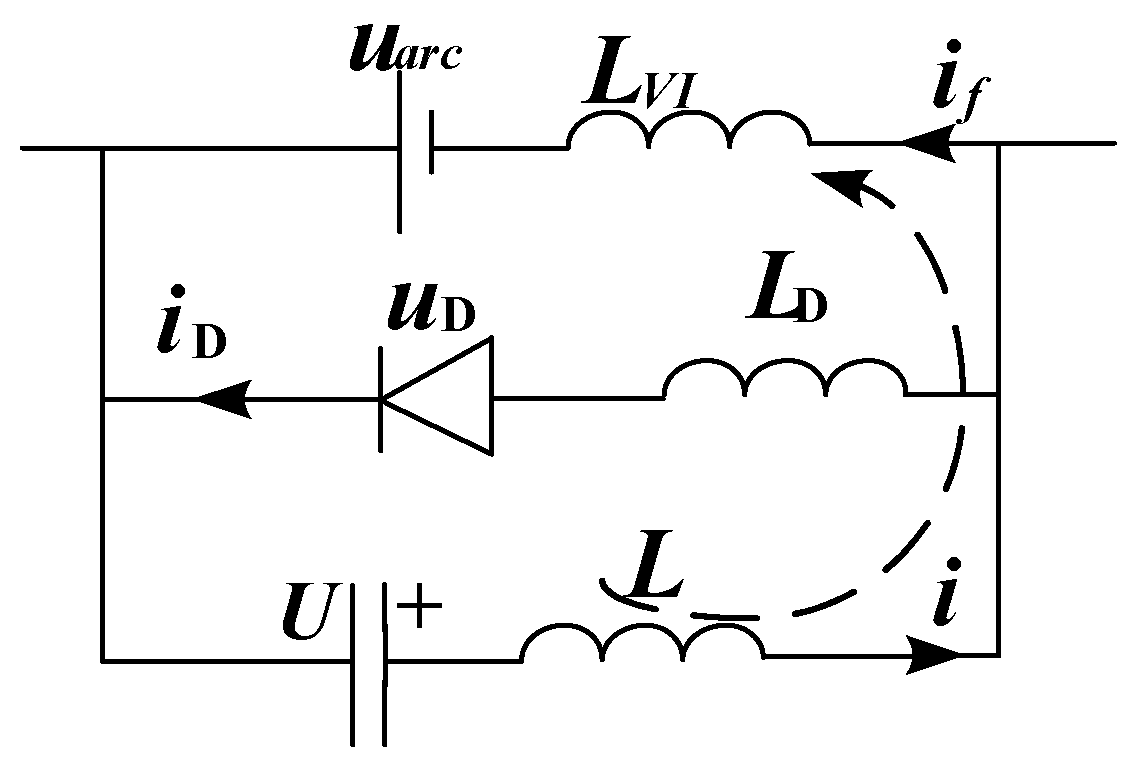
Figure 8.
Selection range of commutation circuit parameters.
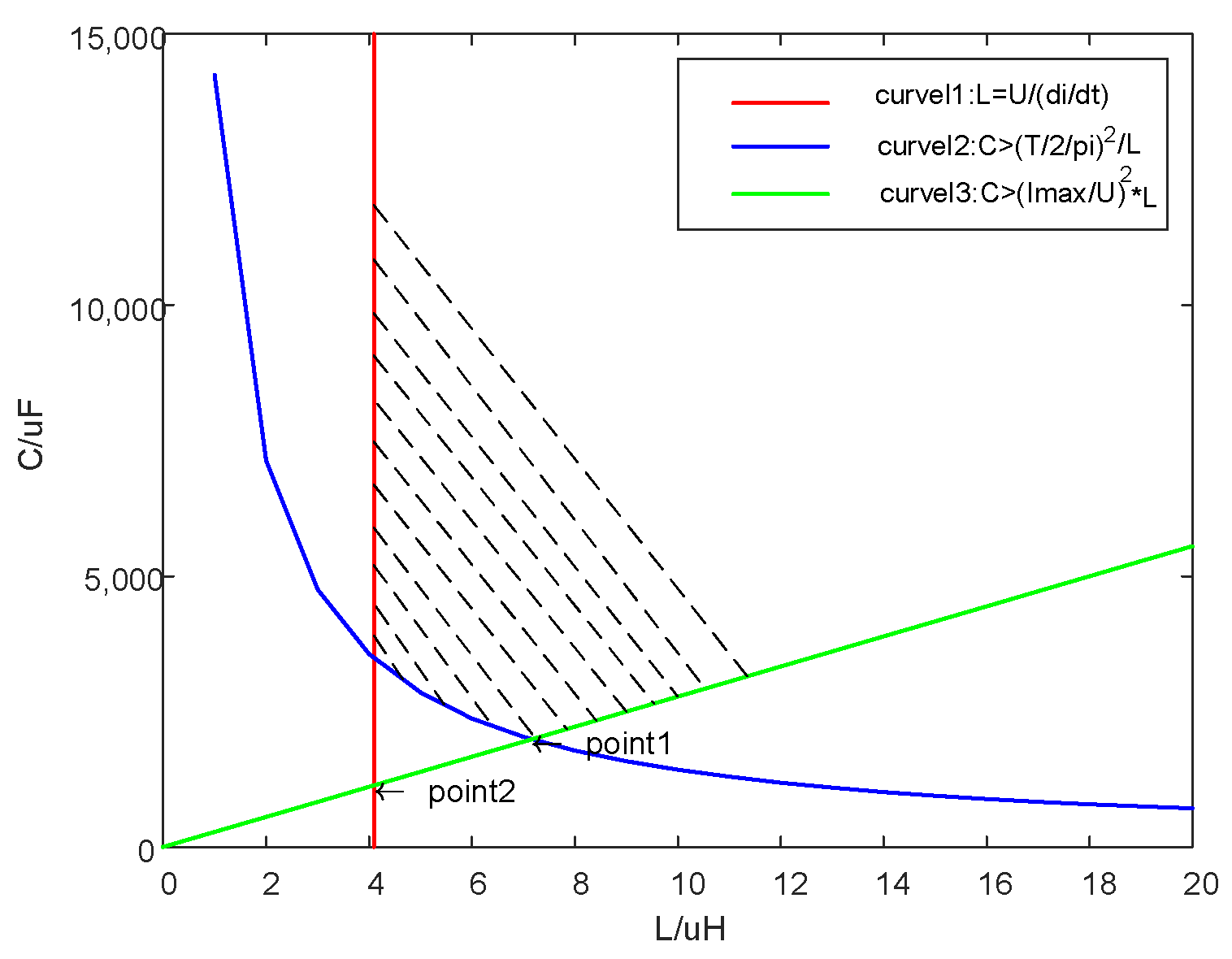
Figure 9.
Selection range of commutation circuit parameters.
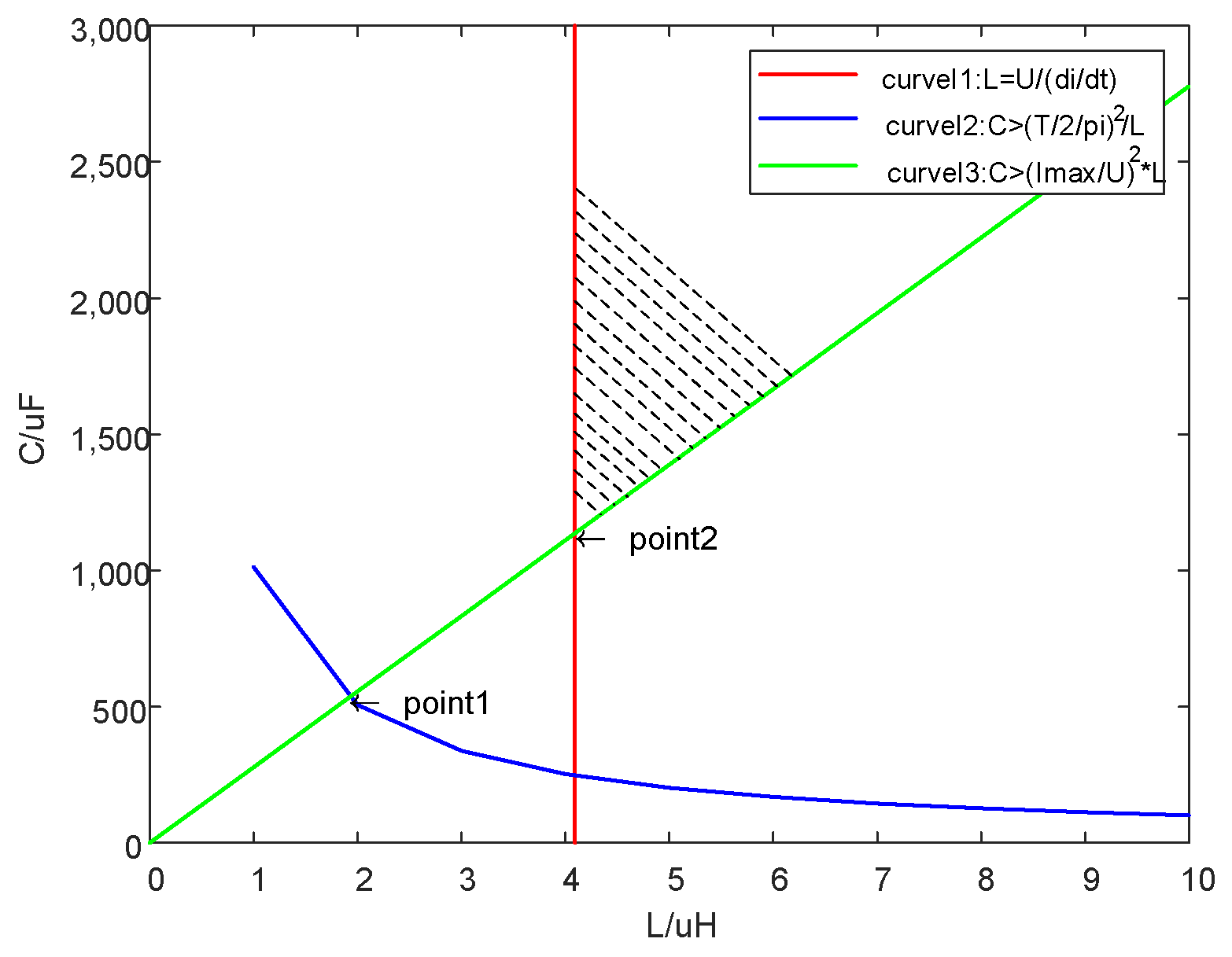
Figure 10.
Schematic diagram of the electromagnetic repulsive vacuum contact. (a) Schematic diagram of the geometry of the contact; (b) schematic of the drive circuit for the repulsive coil.
Figure 10.
Schematic diagram of the electromagnetic repulsive vacuum contact. (a) Schematic diagram of the geometry of the contact; (b) schematic of the drive circuit for the repulsive coil.
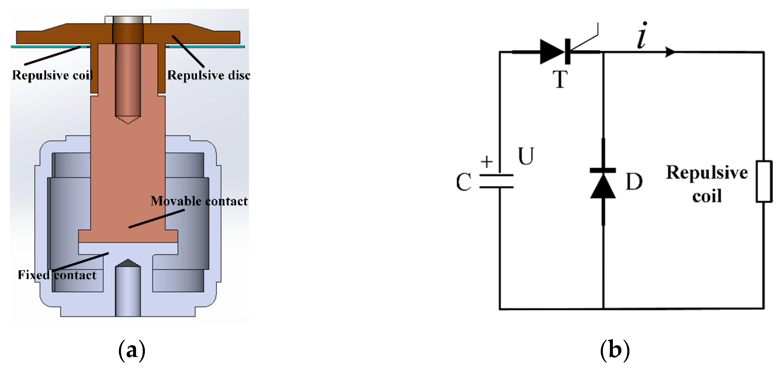
Figure 11.
Schematic diagram of the structure of the ERM.
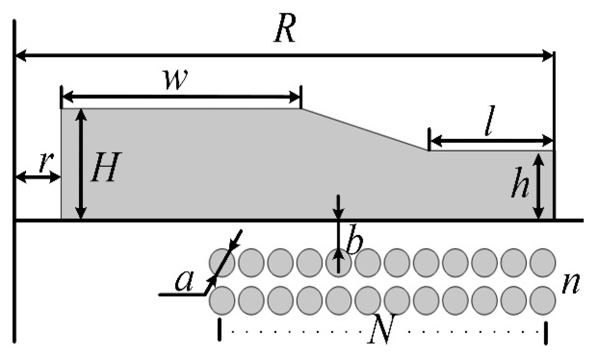
Figure 12.
Displacement curves of contacts under different materials.
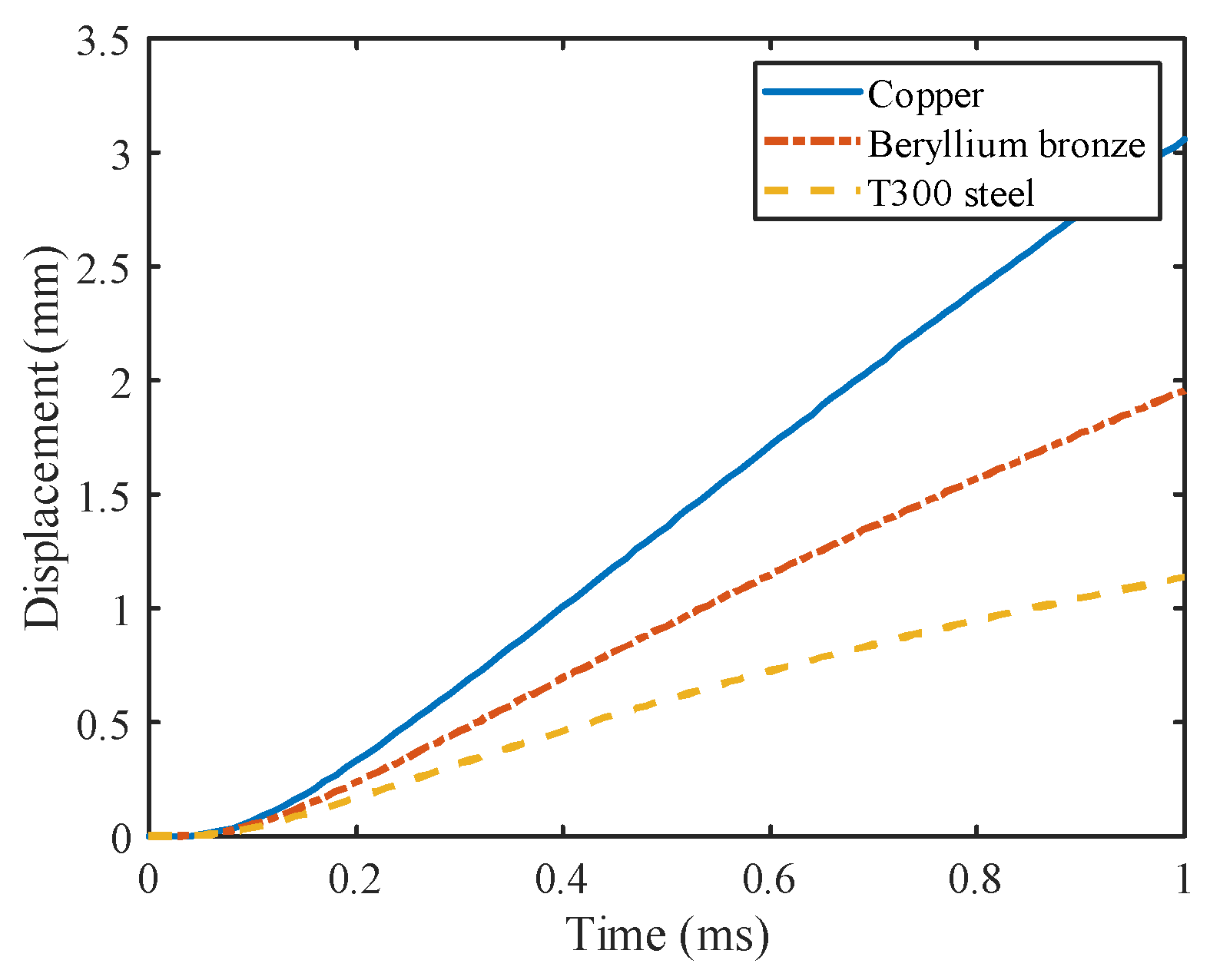
Figure 13.
Distribution diagram of the equivalent stress with different materials.
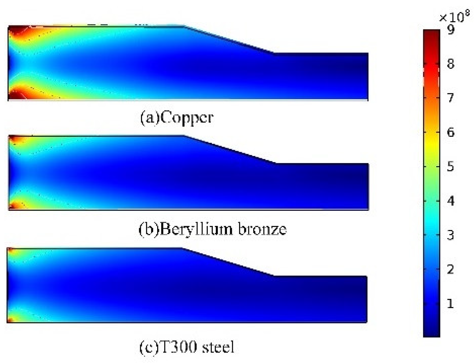
Figure 14.
Structural diagram of experiment platform.
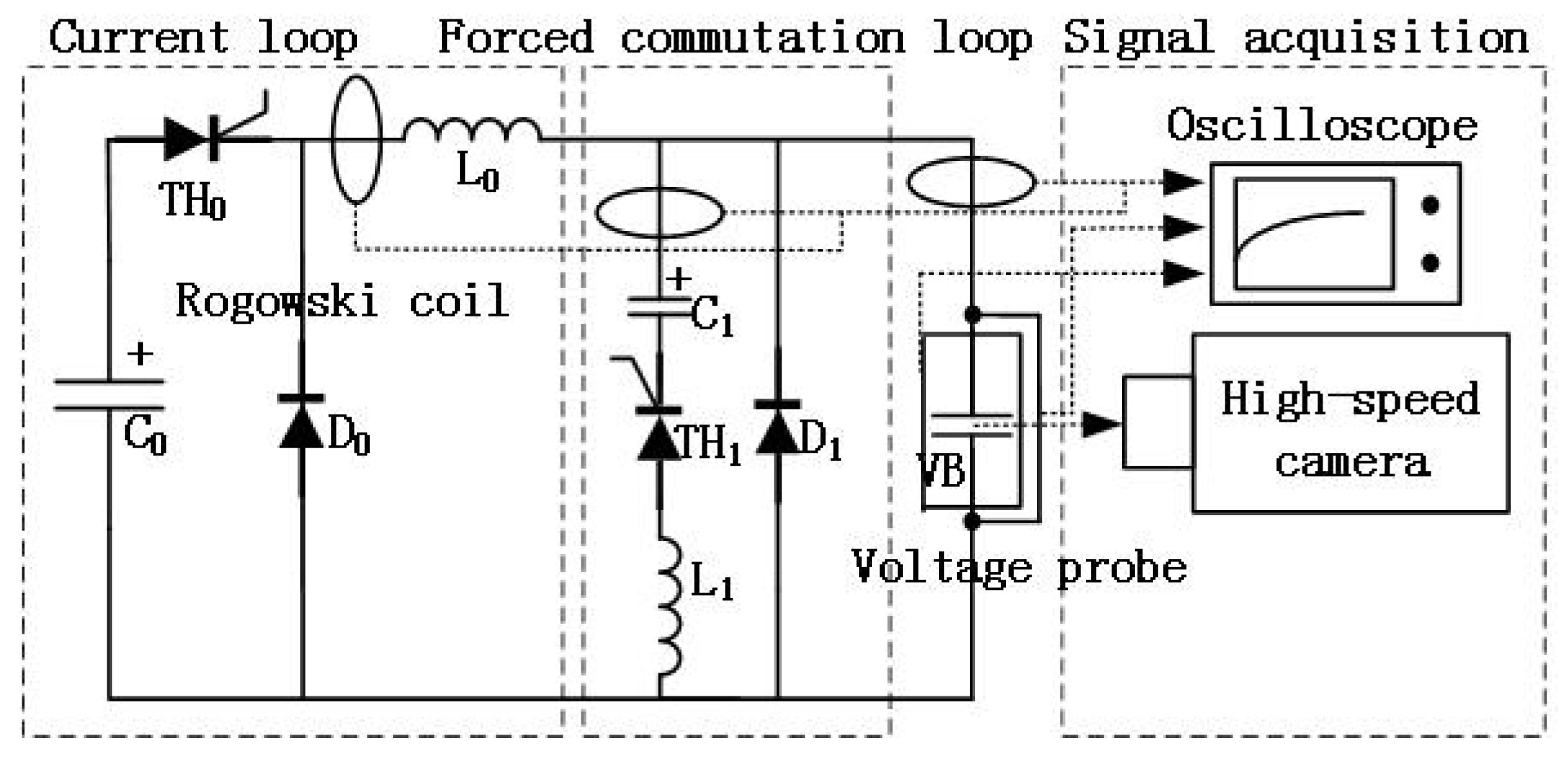
Figure 15.
Picture of the experiment site.
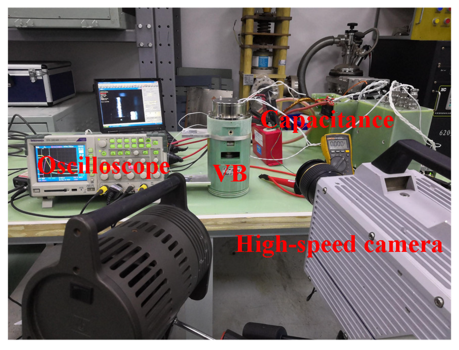
Figure 16.
Simulation and experimental displacement curves of contacts.
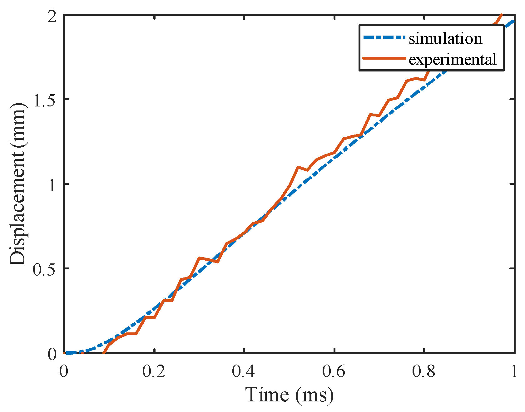
Figure 17.
Current and voltage waveforms during the breaking process of the HDCCLCB.

Table 1.
Structural parameters of the ERM.
| Parameters | Value | Parameters | Value |
|---|---|---|---|
| Internal diameter r/mm | 6 | Number of coils N | 12 |
| External diameter R/mm | 19 | Number of coil layers n | 2 |
| Inside height H/mm | 10 | Wire diameter a/mm | 2 |
| Outside height h/mm | 3 | Gap b/mm | 2 |
| High bench width w/mm | 10 | Capacitive voltage U/kV | 1.7 |
| Low bench width l/mm | 5 | Capacitance C/μF | 200 |
Table 2.
Physical Parameters of Materials.
| Beryllium Bronze | Copper | T300 | |
|---|---|---|---|
| Conductivity /(S/m) | 1.2 × 10⁷ | 5.99 × 10⁷ | 5 × 10⁶ |
| Density /(g/cm3) | 8.3 | 8.9 | 8.0 |
| Yield strength /MPa | 1035 | 70 | 1957 |
| Young’s modulus E/GPa | 130 | 110 | 186 |
| Poisson’s ratio | 0.35 | 0.34 | 0.3 |
Table 3.
Breaking Process Schedule.
| Time | Events |
|---|---|
| 0 μs | Short-circuit fault occurs |
| 100 μs | Fault detection time 100 μs |
| 220 μs | Inherent time of ERM 120 μs |
| 290 μs | Arcing time 70 μs |
| 350 μs | Commutation time 60 μs |
| 500 μs | Zero-voltage time 150 μs |
| 2100 μs | Breaking time 2.1 ms |
Disclaimer/Publisher’s Note: The statements, opinions and data contained in all publications are solely those of the individual author(s) and contributor(s) and not of MDPI and/or the editor(s). MDPI and/or the editor(s) disclaim responsibility for any injury to people or property resulting from any ideas, methods, instructions or products referred to in the content. |
© 2023 by the authors. Licensee MDPI, Basel, Switzerland. This article is an open access article distributed under the terms and conditions of the Creative Commons Attribution (CC BY) license (https://creativecommons.org/licenses/by/4.0/).
Share and Cite
MDPI and ACS Style
Lv, Z.; Wang, X.; Zhuang, J.; Liu, L.; Yuan, Z.; Li, S.; Wu, J. Analysis and Design of the High Current Rising Rate Hybrid DC Current Limiting Circuit Breaker. Electronics 2023, 12, 2657. https://doi.org/10.3390/electronics12122657
AMA Style
Lv Z, Wang X, Zhuang J, Liu L, Yuan Z, Li S, Wu J. Analysis and Design of the High Current Rising Rate Hybrid DC Current Limiting Circuit Breaker. Electronics. 2023; 12(12):2657. https://doi.org/10.3390/electronics12122657
Chicago/Turabian StyleLv, Zhiyong, Xiangjun Wang, Jinwu Zhuang, Luhui Liu, Zhifang Yuan, Siguang Li, and Jin Wu. 2023. "Analysis and Design of the High Current Rising Rate Hybrid DC Current Limiting Circuit Breaker" Electronics 12, no. 12: 2657. https://doi.org/10.3390/electronics12122657
Note that from the first issue of 2016, this journal uses article numbers instead of page numbers. See further details here.