Article

Design and Analysis of Pattern Reconfigurable Antenna Based on RF MEMS Switches

School of Electronic Engineering, Beijing University of Posts and Telecommunications, Haidian District, Beijing 100876, China
*
Author to whom correspondence should be addressed.
Electronics 2023, 12(14), 3109; https://doi.org/10.3390/electronics12143109
Submission received: 5 June 2023 / Revised: 7 July 2023 / Accepted: 13 July 2023 / Published: 17 July 2023

Abstract

:
The research on reconfigurable antennas has some disadvantages such as low working frequency and large size. This paper presents a Ka-band patch antenna with pattern reconfigurability using RF MEMS switches. The antenna contains one main patch, two sub-patches, two parasitic patches, and two RF MEMS switches. By controlling the states of the RF MEMS switches, the antenna can achieve three different radiation patterns (−8°, 0°, and +8°) at 35 GHz. The pattern analysis was based on the electric field vector addition method. The analytical, simulated, and measured results agree well with each other. Due to its compact and thin structure of 3.7 mm × 5.2 mm × 0.4 mm, this antenna can be applied in fields such as satellites, smartphones, etc.

1. Introduction

Reconfigurable antennas are antennas that can change their working modes, such as frequency, radiation pattern, polarization, etc., by shifting the states of switches in the antenna elements and arrays, phase shifters, and T/R (transmit/receive) components while keeping the antenna’s mechanical structure unchanged. This enables one antenna to achieve the functions of multiple antennas. Compared with fixed beam antennas, reconfigurable antennas can adjust their characteristics according to the actual environmental requirements in real time. Pattern reconfigurable antennas mainly control the radiation structure of the antenna using switches to realize the switching of working modes so that the antenna can complete the pattern reconfiguration in a very short time. Various methods have been proposed to achieve reconfigurability, such as PIN diodes [1], copper strips [2], and others. Among these methods, RF MEMS technology offers some distinctive advantages, such as smaller size, higher quality factors, and higher linearity [3]. Therefore, many reconfigurable antennas based on RF MEMS switches have been reported in the literature [4,5,6,7,8,9,10,11,12]. Nevertheless, most of these antennas operate at low frequencies and lack process consistency, as the RF MEMS switches are added to the circuitry after the antenna has been manufactured, rather than being integrated into the same production process as the antenna patch. This leads to poor process consistency and increased complexity and cost. References [13,14,15,16,17] used devices such as PIN diodes and Varactor diodes to reconfigure the antenna pattern. These antennas have large reconfigurable angles of the pattern but their length and width are generally above 10 mm and therefore cannot adapt to the trend of device miniaturization.
In this paper, we introduce a new design for a pattern reconfigurable patch antenna that is specifically tailored for Ka-band applications. Our design incorporates RF MEMS switches, which allow for a wider working range and higher throughput compared to other bands. This makes our antenna an ideal candidate for applications such as 5G mobile communication and satellite communication systems, where there is a need for wider spectrum resources to achieve efficient data transmission.

2. Antenna Structure Design

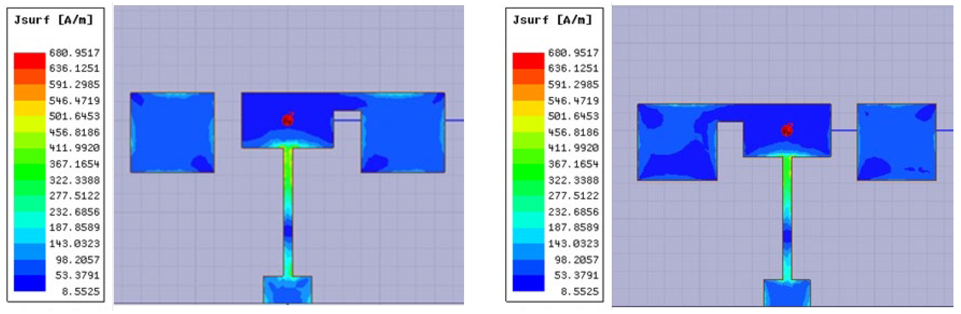
2.1. Current Distribution Analysis

The current direction of the antenna has a direct impact on the spatial distribution of the antenna radiation field. By using the relationship between the source current and the radiation field, we can change the radiation direction of the antenna without changing its frequency, thus achieving a reconfigurable pattern design. To meet the reconfigurable requirements, we need to first determine the current distribution on the antenna, including the current amplitude and phase information, and then select a suitable antenna structure for design according to the current requirements. In the design of reconfigurable antennas, more attention is paid to flexibility and adjustability, and the changes of current distribution under different working conditions need to be fully considered and optimized accordingly. We intended to achieve reconfigurable antenna radiation patterns by changing the antenna structure and thus affecting the current distribution on the antenna’s surface by loading micro-mechanical structures on the antenna.
In order to achieve reconfigurable antenna patterns, this design utilizes two sub-patches placed on either side of the rectangular patch. By controlling the connection between the center patch and the sub-patches using switches, the current distribution of the antenna can be altered. When the switches are in the open state, current flows from the switches to the sub-patches, resulting in a change in the current distribution. Please refer to Figure 1 for a visual representation of the current distribution.
According to the current distribution of the antenna, it can be found that the energy is mainly concentrated at the interface between the feed line and the main patch. When the main patch is connected to the sub-patch, the radiated energy is biased towards the sub-patch side. Therefore, it was preliminarily judged that the design using the main and sub-patches could achieve the reconfiguration of two directions of the antenna.

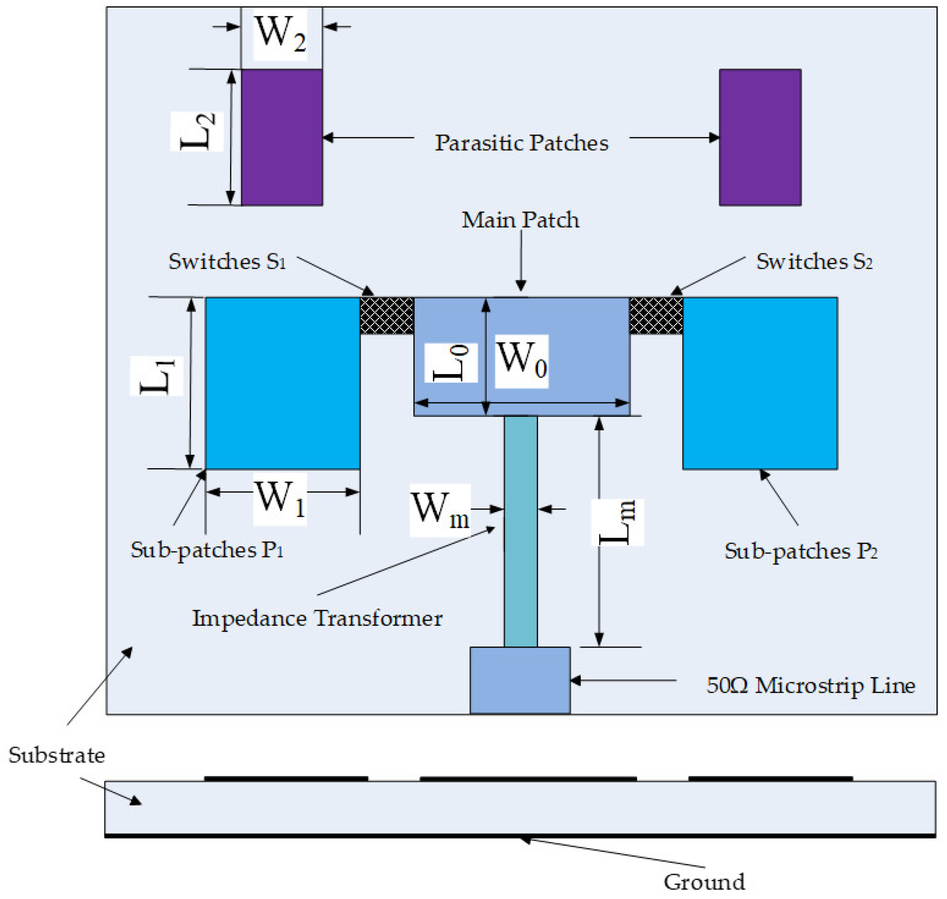
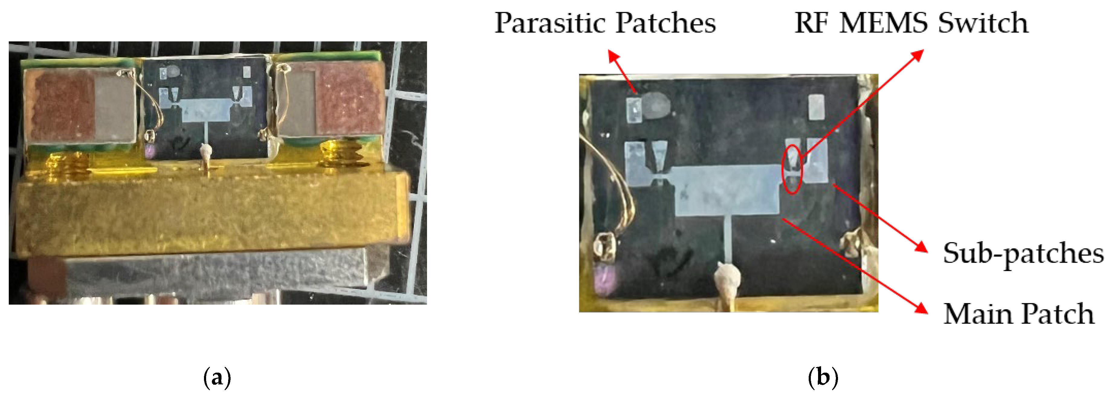
2.2. Main Patch, Sub-Patches and Parasitic Patches Design

The antenna’s center frequency was 35 GHz and it used a high-resistivity silicon substrate that was 400 μm thick and had a relative permittivity of 11.9. The design target was to have a length and width within 6 mm × 5 mm. First, based on the microstrip rectangular patch structure, the main patch was analyzed. The top and side view structures of the rectangular patch are displayed in Figure 2 [8]. The patch’s length L and width W of the rectangular patch can be determined using Formulas (1)–(4) [18], where ε e is the effective permittivity of high-resistivity silicon, ε r is the relative permittivity of high-resistivity silicon, c is the speed of light in vacuum, f is the center frequency of the antenna, h is the substrate thickness, W is the maximum value of the patch width that does not cause field distortion, and L is the patch length considering edge effects.
W = c 2 f ε r + 1 2 = 1.701   m m
ε e = ε r + 1 2 + ε r 1 2 1 + 12 h W 1 2 = 9.086
Δ L = 0.412 h ε e + 0.3 W / h + 0.264 ε e 0.258 W / h + 0.8 = 0.157   m m
L = 1 2 c f ε e 2 Δ L = 1.108   m m .
According to the above calculation, the dimensions of the 35 GHz microstrip rectangular patch antenna were about 1.7 mm × 1.1 mm. In order to achieve reconfigurable antenna patterns, a sub-radiation patch was placed on each side of the rectangular patch, and the main and sub-patches were connected by switches, as shown in Figure 3. The reconfigurable antenna comprised a main patch, two sub-patches, two parasitic patches, two switches, a 50 Ω microstrip line, and an impedance transformer. The switches S1 and S2 were responsible for controlling the connection between the main patch and the two sub-patches located on the left and right sides.
The main patch can be connected to the two sub-patches on the left and right sides, respectively, by manipulating the on–off of the two switches. The antenna could then create three distinct functioning states and its pattern could be reconfigured in three directions. The specific working states of the antenna and the corresponding relationship between the working states of the switches are shown in Table 1. It should be noted that, since the antenna radiation pattern of both switches in the off state was consistent with the antenna radiation pattern of both switches in the on state, the situation in which both switches were in the off state was not considered here.
After adding the sub-radiation patch, the antenna structure became irregular. Therefore, based on the original calculation of the regular rectangular patch size, the size of the main radiation patch and the sub-radiation patch were adjusted and simulated. The results of the simulation are presented in Figure 4. The findings indicate that the size L0 and W0 of the main radiation patch have little effect on the center frequency f0 of the antenna, while the size L1 of the sub-radiation patch has a great influence on the center frequency f0 of the antenna and f0 decreases as L1 increases. Therefore, the working frequency of the antenna can be changed by adjusting the size L1 of the sub-radiation patch, and then other parameters can be optimized.
To ensure good performance of the antenna element, impedance matching must be achieved. Since it is difficult to know the exact impedance value after the antenna design is completed, a 1/4 wavelength impedance transformer was used to match the impedance of the 50 Ω feed line at the input end. This can achieve the ideal impedance matching effect. The simulation results show that, when Wm = 0.38 mm, the antenna and the 1/4 wavelength impedance transformer can achieve matching, which is exactly the width of the 50 Ω microstrip transmission line.
Without affecting the impedance matching, Wm was fine-tuned and the simulation results show that the bandwidth of the antenna decreases as Wm increases, as shown in Figure 5.
Two parasitic patches (the blue portion in Figure 6) were added to the antenna to increase its working bandwidth and enhance its functionality. The parasitic patch can form a resonant circuit, which is equivalent to the occurrence of two or more resonant points. The bandwidth of the antenna can be increased when the resonant frequency of the resonant circuit is close to the antenna’s own resonant frequency. The size of the parasitic patch can also be modeled, simulated, and fine-tuned using the above method, which was not repeated here.
The pattern reconfigurable antenna was thus created. Figure 6 depicts the top view of the antenna, while Table 2 provides the specific dimensions of the antenna.

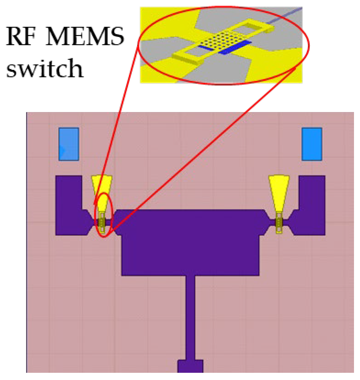
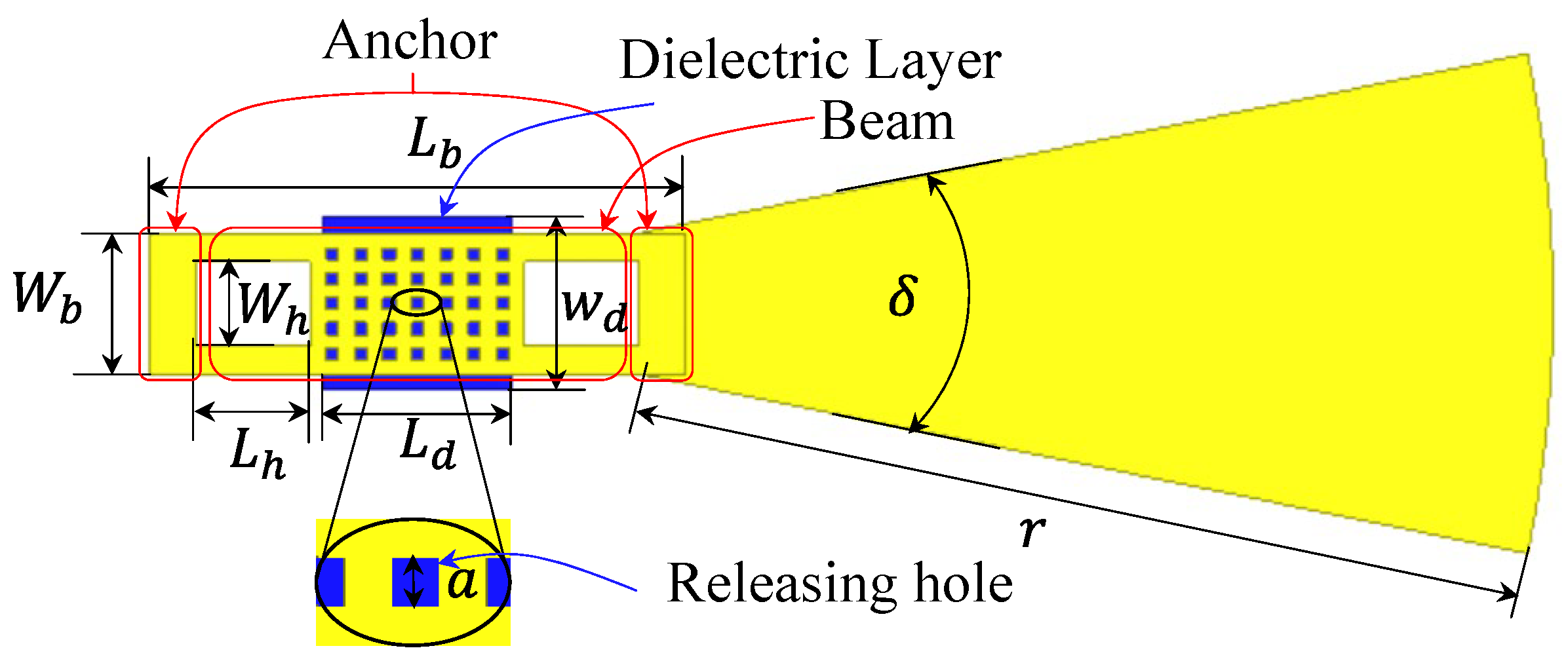
2.3. RF MEMS Switch Design

Compared to other RF switches, MEMS switches have benefits such as low insertion loss and excellent isolation. They play a crucial role in performance tuning for antenna reconfigurability in this paper. Figure 7 depicts the structure of the MEMS shunt capacitive switch, with the beam thickness being 1 μm and the distance g 0 between the beam and the dielectric layer being 1.5 μm. The MEMS switch works by utilizing the electrostatic force generated by the DC voltage to change the distance g 0 , thereby controlling the on–off of the RF signal. When the electrostatic force causes the beam and the dielectric layer to contact, the MEMS switch is closed and in the down state, and the RF signal is cut off. When no DC voltage is applied, the switch is in the up state, and the beam and dielectric layer maintain a distance of 1.5 μm, allowing the RF signal to pass through the transmission line below the beam. In addition, a fan-shaped microstrip line was utilized, with a length of approximately one quarter wavelength of the center frequency. The use of fan-shaped microstrip lines has two functions. One is to make the RF signal see an open circuit at the end of the fan-shaped microstrip line so that the RF signal in the MEMS switch anchor area can smoothly pass through this fan-shaped microstrip line and short-circuit to ground. Another function is to reduce the size of the impedance transformer branch, making the structure of the entire antenna element more compact.
The MEMS switch loaded with the fan-shaped microstrip line was simulated separately and the simulated insertion loss and isolation are shown in Figure 8. Figure 8 shows that, at 35 GHz, the MEMS switch’s isolation can reach 20 dB while its insertion loss is only approximately 0.3 dB, which meets the design requirements and can ensure the performance of the reconfigurable antenna.

3. Theory Analysis

Calculating the current density distribution on the patch and then determining the antenna’s radiation direction using the directivity function is the conventional approach to determining the radiation direction of a microstrip patch antenna. However, it is difficult to obtain the current density at each point on the patch and, even if the current density is obtained, it has to be integrated to obtain the radiation pattern, which makes this method very difficult to use to calculate the radiation direction. The directivity function can be expressed as follows [19].
P θ , φ = J s x , y , z e j k 0 x sin θ cos φ + y sin θ sin φ + z cos θ d v ,
where P θ , φ represents the directivity function of the antenna, x ,   y ,   z represents the coordinates of the radiation source point, k 0 represents the wave number of free space, and v represents the region where the current density J s exists.
Since the above method finds it difficult to solve the radiation direction of the antenna, we proposed the electric field vector addition method to solve the radiation direction of the antenna. Figure 9 shows the electric field distribution of the antenna and the coordinate system used for the vector superposition method calculation (for the sake of simulation and observation, the MEMS switch was replaced by a metal patch here). As shown in Figure 9, the radiation characteristics of the antenna are mainly generated by the gap between the main patch and the sub-patch and the dielectric layer. Whether the MEMS switch on the left is in the up or down state, or the two MEMS switches are combined into other modes, similar results will be obtained. In order to facilitate the solution of the vector superposition method, a coordinate system was established, as shown in Figure 9.
The vector superposition method was used to analyze the radiation characteristics of the antenna, where the far-field of the main patch, the sub-patch, and the parasitic patch can be analyzed by the equivalent magnetic current model [19]. In this model, the vector potential functions F m , F a , and F b , generated by the equivalent magnetic current, represent the potential situation on the main patch, the sub-patch, and the parasitic patch, respectively. The vector potential functions F m , F a and F b can be expressed by Equation (6) [8].
F m z ^ 1 | R | e j k 0 | R | · sin k 0 h sin θ · cos φ k 0 h sin θ · cos φ · sin 1 2 k 0 w m cos θ k 0 cos θ F a z ^ 1 R d 1 e j k 0 R d 1 · sin k 0 h sin θ · cos φ k 0 h sin θ · cos φ · sin 1 2 k 0 w a cos θ k 0 cos θ F b z ^ 1 R d 2 e j k 0 + π R d 2 · sin k 0 h sin θ · cos φ k 0 h sin θ · cos φ · sin 1 2 k 0 w b cos θ k 0 cos θ
where R ,   θ ,   φ is the field point coordinate system; h is the thickness of the substrate; k 0 is the wave number of electromagnetic waves in free space; w m , w a , and w b are the widths of the main patch, the auxiliary patch, and the parasitic patch, respectively; R is the vector from the origin to the observation point (representing the vector of the observation point on the main patch); and d 1 and d 2 are the vectors marked in the Figure 9 (representing the vectors of the observation points on the sub-patch and the parasitic patch, respectively). Since the antenna designed in this paper had a symmetrical structure, according to the duality principle, it can be known that the far-field distribution can be obtained by Equation (7) [8].
E φ = 𝛻 × F m + F a + F b .
The far-field magnetic field can be obtained using two methods—one by solving the Maxwell equations and the other by using the relationship of the far-field plane wave electromagnetic field. Once the far-field was obtained, we could use MATLAB software to plot the radiation pattern of the far-field, as shown in Figure 10. Figure 10a shows the radiation pattern of the reconfigurable antenna calculated according to the above formula and Figure 10b shows the radiation pattern of the reconfigurable antenna simulated by HFSS software. It can be seen from Figure 10 that the two results are very consistent. However, it should be noted that the radiation pattern obtained by the formula calculation has no back lobe, while the antenna radiation pattern obtained by HFSS software simulation has a back lobe. This is because the result of the formula calculation is based on a simplified mathematical model. However, only focusing on the main radiation direction angle and ignoring the existence of the back lobe does not affect the final calculation result, which shows that the spatial electric vector superposition method analysis method proposed in this section is effective.

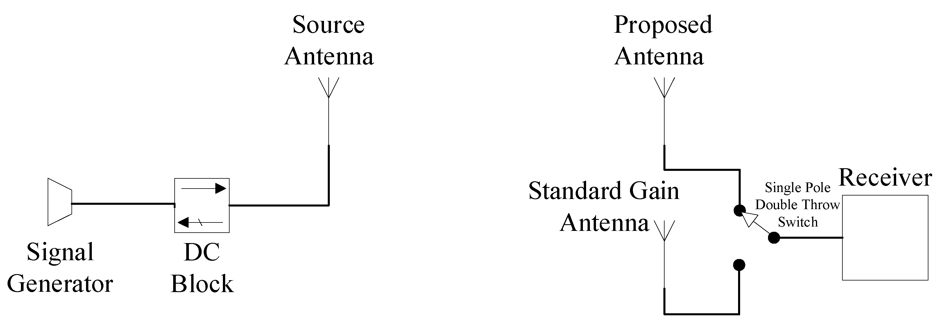
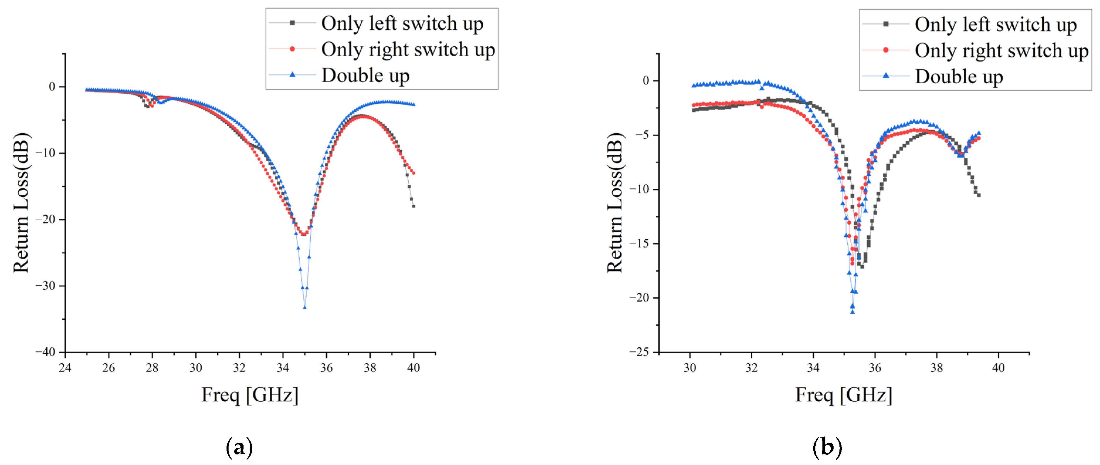
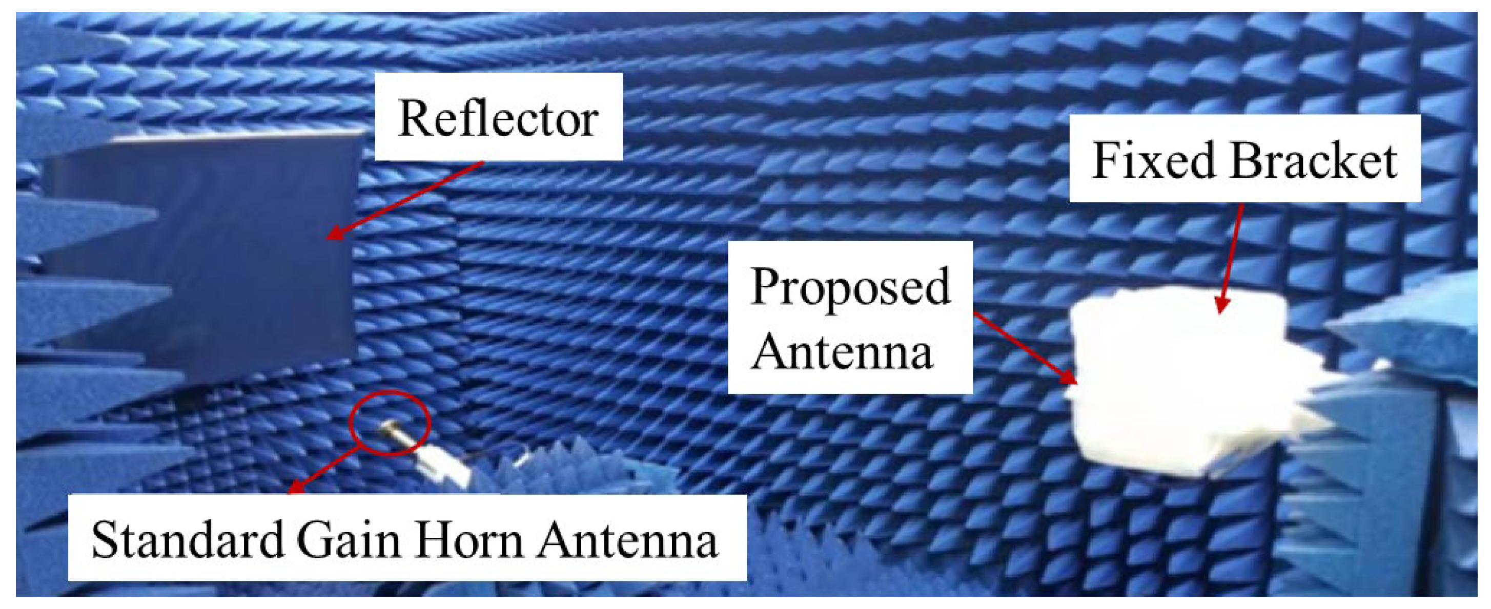
4. Measurement and Results

After the antenna design and simulation were completed, the layout of the antenna was made and processed. A 400 μm thick, 11.9 relative permittivity, high-resistivity silicon surface was used to create the antenna structure. First, a thermal oxidation method was used to form a SiO2 thin film with a thickness of 0.3 μm on the surface of the high-resistivity silicon as an insulating layer. Second, 0.2 μm thick aluminum was deposited on the silicon wafer and formed into direct current bias feeding points according to the preset pattern. Next, SiAl with a thickness of about 0.05 μm was used to make the bias lines. Then, a dielectric layer with a thickness of 1500 Å of Si3N4 was prepared by PECVD on top of the electrodes and bias lines. After that, evaporation was performed to form a MEMS switch anchor area with a thickness of 1.5 μm. Then, chemical mechanical polishing (CMP) was used to reduce the thickness of the polyimide sacrificial layer from 5 μm to 1.3 μm and aluminum with a thickness of 0.6 μm was used to make the MEMS switch beam. Finally, plasma dry release technology was used for full-chip release to ensure that the switch beam would not collapse. Figure 11 shows the antenna after fabrication.
The pattern reconfigurable antenna designed in this paper works at 35 GHz, a frequency point at which impedance matching is critical for antenna performance. The return loss of the antenna needs to be measured, which is carried out by a vector network analyzer (R&S ZVA50, Rohde&Schwarz, Munich, Germany). Figure 12 shows the simulation and measurement results of the return loss of the antenna. According to the simulation results, the antenna is capable of switching among three working modes while maintaining a return loss greater than 20 dB in all three modes. When both switches are in the on state, the 10 dB bandwidth is about (36 − 33.2)/35 = 8%, which far exceeds the design requirements. It is worth noting that the measurement results indicate a return loss greater than 17 dB in all three modes, and the 10 dB bandwidth is approximately (36.1 − 35.25)/35 = 2.4%. The shapes of the return loss curves in both simulation and measurement results are very similar, which verifies the correctness of this design. Due to the use of fixtures in the test and the influence of processing technology and other factors, the return loss of the measurement results is not as good as the simulation effect, which is the main reason for the gap.
The radiation pattern of the reconfigurable antenna in each working mode was tested in the microwave anechoic chamber after the return loss of the antenna was evaluated. For the antenna gain measurement in this paper, we adopted the comparison method. The test steps are as follows.
(1)
Connect the test system according to Figure 13 and power on the instrument equipment for preheating;
(2)
Calibrate the instrument and set the instrument parameters correctly, set the signal source and make the radiation direction of the transmitting antenna point to the gain reference antenna and the direction of the pattern reconfigurable antenna to be tested, turn on the DC bias power supply and make the pattern reconfigurable antenna enter one of the reconfigurable working modes;
(3)
Turn on the transmitting antenna and make it emit a constant power signal, adjust the position of the antenna to be tested so that its direction faces the direction of the signal transmitted by the transmitting antenna, and record the signal power intensity P A U T received by the spectrum analyzer connected to the reconfigurable antenna to be tested. Place the reconfigurable antenna to be tested near the gain reference antenna, place the gain reference antenna on a slide that can move at a constant speed, and slide the gain reference antenna up and down to measure the power P r e f of the electromagnetic wave received in space due to reflection with the gain reference antenna;
(4)
The gain value G A U T of the pattern reconfigurable antenna at this point and angle can be calculated by formula (8), where G r e f is the gain of the gain reference antenna, and the values here are expressed in logarithms:
G A U T = G r e f + P A U T P r e f ;
(5)
By measuring the gain values at multiple angles and frequency points using the above method, we can obtain the pattern and gain of the pattern reconfigurable antenna to be tested.
Figure 13. Principle block diagram of comparative law method for measuring the gain of reconfigurable antenna.
Electronics 12 03109 g013
Figure 14 is the picture of microwave anechoic chamber and the test results are shown in Figure 15. The test results show that the antenna can switch among three working modes; the main lobe radiation directions of the three working modes are −0.6°, −7.9°, 8.0°. Therefore, the reconfigurable antenna designed in this paper can achieve directional pattern switching of the main lobe to the left (about −8°), middle (about 0°), and right (about +8°).
The performance comparison between the reconfigurable antenna developed in this paper and other reconfigurable antennas is shown in Table 3. From Table 3, it can be seen that we designed a MEMS pattern reconfigurable antenna that can dynamically adjust the antenna radiation direction at a working frequency of 35 GHz. Moreover, we designed the antenna and MEMS switch integrated design and fabrication technology, which makes the whole antenna more compact and easy to integrate and apply. The comparison data show that the pattern reconfigurable antenna designed and presented in this paper can effectively achieve the purpose of device miniaturization while ensuring good radio frequency performance parameters and improving the flexibility and adaptability of the antenna.

5. Conclusions

This paper proposed a patch antenna with pattern reconfigurability using RF MEMS switches. The antenna has a compact and thin structure of 3.7 mm × 5.2 mm × 0.4 mm and can achieve three different radiation patterns (−8°, 0°, and +8°) at 35 GHz by controlling the states of the RF MEMS switches. The pattern analysis was based on the electric field vector addition method. Compared with other pattern reconfigurable antennas, the antenna design presented in this paper effectively reduces antenna size by over 50% while achieving multi radiation direction reconfigurability.
At the same time, the antenna design presented in this paper also has some problems, such as the reconfigurable angle of the antenna not being large enough. A large reconfigurable angle is better for the reconfigurable antenna as it can cover a wider spatial area, improving the signal coverage and reliability. Future work needs to be undertaken in this respect.

Author Contributions

Y.W. conceived and designed the study, performed the structure optimization, model simulation, data analysis, and wrote the manuscript. Z.D. is the person in charge of the supporting project. C.L. assisted with the literature search and chart drawing. All authors have read and agreed to the published version of the manuscript.

Funding

The project was supported by the Fund of State Key Laboratory of Information Photonics and Optical Communications (Beijing University of Posts and Telecommunications) (No. IPOC2022ZT02), China.

Data Availability Statement

Not applicable.

Conflicts of Interest

The authors declare no conflict of interest.

References

  1. Alam, M.; Abbosh, A. Wideband Pattern Reconfigurable Antenna Using Pair of Radial Radiators on Truncated Ground with Switchable Director and Reflector. IEEE Antennas Wirel. Propag. Lett. 2016, 16, 24–28. [Google Scholar] [CrossRef]
  2. Pan, Y.; Ma, Y.; Xiong, J.; Hou, Z.; Zeng, Y. A compact antenna with frequency and pattern reconfigurable characteristics. Microw. Opt. Technol. Lett. 2015, 57, 2467–2471. [Google Scholar] [CrossRef]
  3. Dussopt, L.; Rebeiz, G.M. Intermodulation distortion and power handling in RF MEMS switches, varactors, and tunable filters. IEEE Trans. Microw. Theory Tech. 2003, 51, 1247–1256. [Google Scholar] [CrossRef]
  4. Zhou, L.; Sharma, S.K.; Kassegne, S.K. Reconfigurable microstrip rectangular loop antennas using RF MEMS switches. Microw. Opt. Technol. Lett. 2008, 50, 252–256. [Google Scholar] [CrossRef]
  5. Rajagopalan, H.; Kovitz, J.M.; Rahmat-Samii, Y. MEMS reconfigurable optimized e-shaped patch antenna design for cognitive radio. IEEE Trans. Antennas Propag. 2014, 62, 1056–1064. [Google Scholar] [CrossRef]
  6. Al-alaa, M.A.; Elsadek, H.A.; Abdallah, E.A.; Hashish, E.A. Pattern and frequency reconfigurable monopole disc antenna using PIN diodes and MEMS switches. Microw. Opt. Technol. Lett. 2014, 56, 187–195. [Google Scholar] [CrossRef]
  7. Kovitz, J.M.; Rajagopalan, H.; Rahmat-Samii, Y. Design and implementation of broadband MEMS RHCP/LHCP reconfigurable arrays using rotated E-shaped patch elements. IEEE Trans. Antennas Propag. 2015, 63, 2497–2507. [Google Scholar] [CrossRef]
  8. Nadh, B.P.; Madhav, B.T.P.; Kumar, M.S.; Kumar, T.A.; Rao, M.V.; Reddy, S.S.M. MEMS-based reconfigurable and flexible antenna for body-centric wearable applications. J. Electromagn. Waves Appl. 2022, 36, 1389–1403. [Google Scholar] [CrossRef]
  9. Lago, H.; Zakaria, Z.; Jamlos, M.F.; Soh, P.J. A wideband reconfigurable folded planar dipole using MEMS and hybrid polymeric substrates. AEU-Int. J. Electron. Commun. 2019, 99, 347–353. [Google Scholar] [CrossRef]
  10. Erdil, E.; Topalli, K.; Unlu, M.; Civi, O.A.; Akin, T. Frequency tunable microstrip patch antenna using RF MEMS technology. IEEE Trans. Antennas Propag. 2007, 55, 1193–1196. [Google Scholar] [CrossRef]
  11. Abdulkawi, W.M.; Sheta, A.F.A.; Malik, W.A.; Rehman, S.U.; Alkanhal, M.S. RF MEMS switches enabled H-shaped beam reconfigurable antenna. Appl. Comput. Electromagn. Soc. J. (ACES) 2019, 34, 1312–1319. [Google Scholar]
  12. Kim, I.; Rahmat-Samii, Y. RF MEMS Switchable Slot Patch Antenna Integrated With Bias Network. IEEE Trans. Antennas Propag. 2011, 59, 4811–4815. [Google Scholar] [CrossRef]
  13. Khairnar, V.V.; Kadam, B.V.; Ramesha, C.K.; Gudino, L.J. A reconfigurable parasitic antenna with continuous beam scanning capability in H-plane. AEU-Int. J. Electron. Commun. 2018, 88, 78–86. [Google Scholar] [CrossRef]
  14. Ayoub, F.; Tawk, Y.; Woehrle, C.; Costantine, J.; Christodoulou, C. Reconfigurable Cyclical Patch Antenna. In Proceedings of the IEEE International Symposium on Antennas and Propagation & USNC/URSI National Radio Science Meeting, Vancouver, BC, Canada, 19–24 July 2015; pp. 2249–2250. [Google Scholar]
  15. Nguyen, D.-T.; Siragusa, R.; Tedjini, S. Beam steering patch antenna using reactive loading and Yagi-antenna concept. Microw Opt. Technol. Lett. 2015, 57, 417–421. [Google Scholar] [CrossRef]
  16. Zhang, Z.L.; Wu, B. Radiation pattern reconfigurable antenna using double layer tunable graphene superstrate. In Proceedings of the 2015 Asia-Pacific Microwave Conference (APMC), Nanjing, China, 6–9 December 2015; pp. 1–3. [Google Scholar]
  17. Li, K.; Cai, Y.M.; Yin, Y.; Hu, W. A wideband E-plane pattern reconfigurable antenna with enhanced gain. Int. J. RF Microw. Comput.-Aided Eng. 2019, 29, 21530. [Google Scholar] [CrossRef]
  18. Balanis, C.A. Antenna Theory: Analysis and Design; John Wiley & Sons: New York, NY, USA, 2016. [Google Scholar]
  19. Kumar, G.; Ray, K. Broadband Microstrip Antennas; Artech House: London, UK, 2002. [Google Scholar]
  20. Di Palma, L.; Clemente, A.; Dussopt, L.; Sauleau, R.; Potier, P.; Pouliguen, P. 1-Bit Reconfigurable Unit-Cell for Ka-Band Transmitarrays. IEEE Antennas Wirel. Propag. Lett. 2016, 15, 560–563. [Google Scholar] [CrossRef]
  21. Abdulkawi, W.M.; Malik, W.A.; Sheta, A.F.A.; Alkanhal, M.A. A compact dual circular patch pattern reconfigurable antenna. Microw. Opt. Technol. Lett. 2018, 60, 2762–2768. [Google Scholar] [CrossRef]
Figure 1. Surface current distribution of reconfigurable pattern antenna.
Electronics 12 03109 g001
Figure 2. Schematic diagram of the dimensions of the microstrip rectangular patch. (a) Vertical view; (b) Side view.
Electronics 12 03109 g002
Figure 3. Schematic diagram of the reconfigurable antenna (top view in the upper picture and side view in the bottom figure).
Electronics 12 03109 g003
Figure 4. The relationship between the size of the main patch, the sub-patch, and the center frequency of the antenna. (a) The relationship between L0 and f0; (b) The relationship between W0 and f0; (c) The relationship between L1 and f0; (d) The relationship between W1 and f0.
Electronics 12 03109 g004
Figure 5. The relationship between the width of the impedance transformer and the bandwidth of the antenna.
Electronics 12 03109 g005
Figure 6. Top view of the antenna.
Electronics 12 03109 g006
Figure 7. Structure diagram of the MEMS switch.
Electronics 12 03109 g007
Figure 8. S21 of the MEMS switch loaded with the fan-shaped microstrip line. (a) Insertion loss; (b) Isolation.
Electronics 12 03109 g008
Figure 9. The electric field distribution of the antenna and the coordinate system used for the vector superposition method calculation.
Electronics 12 03109 g009
Figure 10. Radiation pattern of the reconfigurable antenna. (a) Theoretical calculation results of the radiation pattern; (b) Simulation results of the radiation pattern.
Electronics 12 03109 g010
Figure 11. Physical picture of the antenna. (a) Antenna with a test fixture; (b) An enlarged view of the antenna.
Electronics 12 03109 g011
Figure 12. The graph of the return loss of the reconfigurable antenna. (a) Simulated return loss. (b) Measured return loss.
Electronics 12 03109 g012
Figure 14. Microwave anechoic chamber.
Electronics 12 03109 g014
Figure 15. The measured results of the directional pattern and gain of the reconfigurable antenna in three working modes. (a) Double up; (b) Only left switch up; (c) Only right switch up.
Electronics 12 03109 g015
Table 1. Corresponding relationship between antenna working state and switch state.
Antenna Working StateSwitch State
1Switch S1 is on, switch S2 is off.
2Switch S1 is off, switch S2 is on.
3Switch S1 is on, switch S2 is on.
Table 2. The physical size of the antenna.
SymbolDescriptionValue
W0width of the main patch900 μm
L0length of the main patch1500 μm
W1width of the sub-patch400 μm
L1length of the sub-patch890 μm
W2width of the parasitic patch300 μm
L2length of the parasitic patch450 μm
Wmwidth of the impedance transformer110 μm
Lmlength of the impedance transformer1300 μm
Wnwidth of the 50 Ω microstrip line190 μm
Lnlength of the 50 Ω microstrip line380 μm
Wbwidth of the switch beam90 μm
Lblength of the switch beam340 μm
Whwidth of the hole54 μm
Lhlength of the hole72 μm
alength of releasing hole8 μm
rlength of the sector stub575 μm
δangle of the sector stub25°
Table 3. Performance comparison.
LiteratureMeansFrequencyReconfigurable AnglesBlock Volume (mm3)
[20]PIN diodes27.5 GHz45°5.1 × 5.1 × 1.274
[13]Varactor diode2.43 GHz80°80 × 140 × 1.6
[14]PIN diodes27 GHz60°9.5 × 9.5 × 1
[15]Varactor diode0.865 GHz48°150 × 500 × 3.18
[16]Tunable Graphene Superstrate30 GHz30°16 × 16 × 10.3
[17]PIN diodes2.5 GHz60°-
[8]MEMS switches2.5 GHz and 5.4 GHz40 × 28 × 0.1
[9]MEMS switches9.41 GHz60°50.8 × 27.5 × 3.68
[10]MEMS switches16.05~15.75 GHz-12.6 × 8.6 × 0.5
[11]MEMS switches1.8 GHz-37 × 72 × 1.75
[21]PIN diodes1.3~1.8 GHz270°24 × 40 × 1.57
[12]MEMS switches4.57 GHz and 4.88 GHz-40 × 40 × 0.25
[5]MEMS switches2~3.2 GHz-120 × 100 × 10
This paperMEMS switches35 GHz16°3.7 × 5.2 × 0.4
Disclaimer/Publisher’s Note: The statements, opinions and data contained in all publications are solely those of the individual author(s) and contributor(s) and not of MDPI and/or the editor(s). MDPI and/or the editor(s) disclaim responsibility for any injury to people or property resulting from any ideas, methods, instructions or products referred to in the content.

