Review

Research Progress in Failure Mechanism and Health State Evaluation Index System of Welded IGBT Power Modules

1
School of New Energy and Power Engineering, Lanzhou Jiaotong University, Lanzhou 730070, China
2
State Key Laboratory of Large Electric Drive System and Equipment Technology, Tianshui 741020, China
*
Author to whom correspondence should be addressed.
Electronics 2023, 12(15), 3248; https://doi.org/10.3390/electronics12153248
Submission received: 5 June 2023 / Revised: 5 July 2023 / Accepted: 24 July 2023 / Published: 27 July 2023

Abstract

:
As the performance requirements of insulated gate bipolar transistors (IGBTs) in various fields of power electronic systems are increasing, the IGBT power module package structure, aging mechanism analysis, and selection of health state characteristic parameters are of great significance to ensure the normal operation of power systems. At present, research on the aging failure of welded IGBT modules is relatively comprehensive and can be divided into chip aging failure and package aging failure according to their failure parts. However, there is some research on the relationship between aging failure and the characteristic quantity of power modules, but no definite system has been formed. Therefore, in this paper, the packaging structure of the solder-type IGBT modules and the aging mechanism caused by different aging reasons were summarized. Moreover, the health status monitoring of solder-type IGBT modules from the junction temperature, bonding line, solder layer, and package insulation aging health status monitoring and its quantitative assessment research progress was analyzed in detail. Also, the health state evaluation index system of the solder-type IGBT modules was completed on the basis of voltage, current, thermal, insulation parameters, and other characteristic quantities. Finally, based on the analysis of domestic and international research problems, the development trend and direction of the condition monitoring technology of solder-type IGBT modules is foreseen. The research on condition monitoring for welded IGBT module technology has a certain significance.

1. Introduction

The efficient use of green energy is an important way to achieve the goal of “carbon neutrality” [1]. Insulated gate bipolar transistors (IGBT) have the advantages of fast switching speed, low driving power, low saturation voltage, high self-protection capability, and flexible control. It has been the core component for new energy, rail transportation, electric vehicles, industrial applications, and household appliances [2]. The core components of these devices have been used in new energy, rail transportation, electric vehicles, industrial applications, and household appliances [2]. With the increasing in operating life, a large number of IGBT modules suffer from electro-thermal fatigue stress and gradual fatigue failure, which affects the normal operation of the system. Therefore, it is necessary to study the fatigue aging mechanism and condition monitoring technology of IGBT modules to ensure the reliable operation of the system [3].
Solder IGBT modules are a common package type that is widely used in industrial and transportation traction applications [4]. The most important feature of this package-type module is that its base is completely insulated, which makes it easy to mount to the heat sink and can significantly reduce the application cost of the module, which is widely used. Owing to the comprehensive cumulative effects of electricity, heat, and force caused by long-term power cycles, solder-type IGBT modules are prone to failure during operation. The failure modes can be divided into chip-level failure and package-level failure. Chip-level failure can directly lead to module destruction, mainly in the form of electrical overstress and the latch-up effect [5,6], which is mainly caused by high temperature and electrical stress inside the device, where the high temperature originates from an abnormal short-circuit current and local packaging defects, while electrical stress originates from collector voltage overshoot and gate electrostatic damage during the switching process of the IGBT. Studies have shown that package-level failure is the main cause of the aging failure of IGBT modules and is the result of a combination of factors [7]. When IGBT modules operate, each layer of material is subjected to different temperature and temperature gradient stresses, and the difference in the coefficient of thermal expansion (CTE) among the materials, that is, the difference in the change in the value of the length quantity owing to the change in the unit temperature of the materials, causes the materials to generate unevenly distributed mechanical stresses under thermal stress [8,9]. Alternating mechanical stresses between materials under long-term cyclic thermal loading of the module under complex operating conditions can cause aging failure of the module. Based on the establishment of an electrical–thermal multi-physical field model of IGBT devices, Li Jie and Lai Wei et al. analyzed the characteristic parameters of IGBT devices under different control conditions, and the results show that the junction and shell temperatures of IGBTs increase more significantly with the shedding of the solder layer and the junction temperature of IGBTs can be used to monitor their health status [10]. Li Yaping and Zhou Luowei et al. cut the bonding wires one by one to simulate the aging of the IGBT module to obtain the saturation voltage drop VCE(sat) under different operating conditions, and the study shows that the saturation voltage drop VCE(sat) of IGBT can be used as an aging characterization parameter [11]. In addition, the gate voltage waveform at the turn-on instant of the IGBT device can also be used as a temperature-sensitive parameter for real-time monitoring of the junction temperature of the IGBT module, which in turn can be used to obtain the health status of the module [12]. Zhao Zixuan and Chen Jie et al. found that the selection of a larger load current during the power cycle aging of IGBT modules accelerates the aging of module bonding wires [13]. The analyzed literature [14] revealed that IGBT module aging is affected by a combination of factors, and the characteristic parameters of IGBT modules can characterize multiple aging mechanisms of the modules. The core of the previously analyzed physical characteristic quantities lies in establishing the correspondence with the thermal parameters, and the literature [15] proposes that the variation of the thermal resistance of the IGBT module can be monitored by detecting the fifth harmonic content of the converter output current. The literature [16] proposes to monitor the variation of the device’s thermal resistance using the shell-to-ambient temperature.
According to the current IGBT module health status monitoring problems, this paper first explains the current failure reasons of the module by introducing the package structure of the IGBT module and then summarizes several commonly used health status monitoring methods of the IGBT module and analyzes the advantages and disadvantages of various methods. Finally, a complete set of health status evaluation index systems of welded IGBT modules is established for the selection of characteristic parameters and health status evaluation of welded IGBT modules.

2. Packaging Structure and Aging Mechanism of Solder Type IGBT Module

To analyze the changes in the corresponding characteristic parameters of welded IGBTs when failures occur, we start with the basic structure and principle of welded IGBTs, understand the operating characteristics of IGBTs, understand the changes in the internal structure and parameters of the modules when different failure failures occur, and then understand the characteristics of their failure.

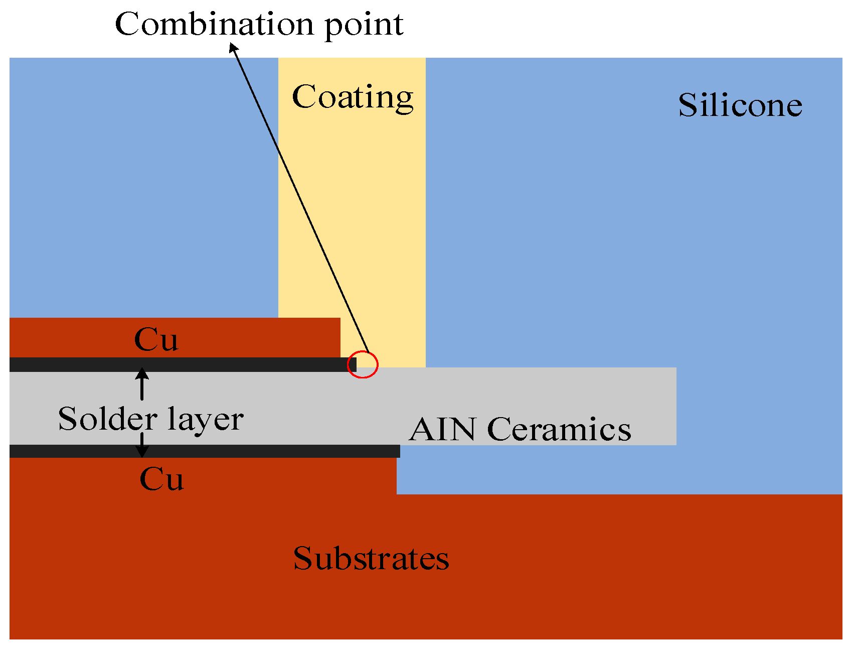
2.1. Package Structure of Solder Type IGBT Module

Soldered IGBT modules are mainly composed of aluminum bonded leads, silicon chips, solder layers, copper layers, ceramic layers, substrates, and potting materials, as shown in Figure 1, where the red color indicates the part that is easy to age [17]. The upper copper layer acts as a conducting current, while the lower copper layer ensures that the copper-clad ceramic plate DCB substrate is flat and smooth, the solder layer is for bonding and fixing the adjacent layers, the ceramic layer has a better heat dissipation effect, and the bottommost copper substrate is hard and smooth, which enhances the hardness and heat dissipation of the module after encapsulation and is easy to install on the heat sink [18].
The main packaging insulating materials for IGBT modules include potting and substrate insulating materials. Gel as an insulating material for IGBT modules places high demands on gel encapsulation technology. At the junction of the copper-clad ceramic plate, metal substrate, and gel, an inhomogeneous electric field is created due to the fact that each material has a different potential [19]. During the operation of the IGBT module, the chip generates power loss generating heat, which passes through the multilayered structure to reach the heatsinks generating a fluctuation in the junction temperature [20]. This causes the bonding wire to fall.

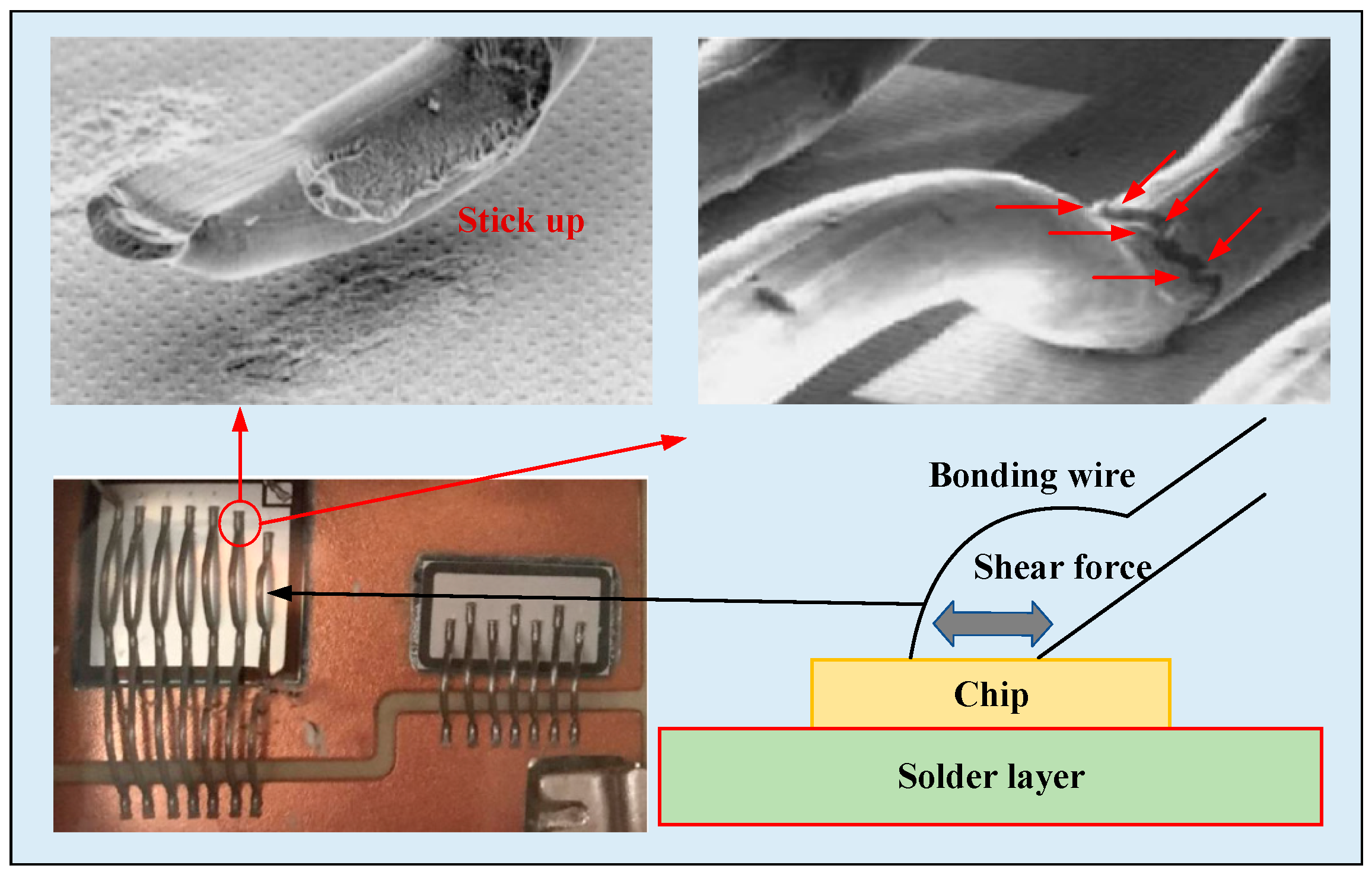
2.2. Analysis of Failure Mechanism for Welded IGBT Modules

2.2.1. Main Causes of Device Failure

1
Characteristics of device failure caused by temperature;
Among the various factors that cause device failure, temperature has the largest proportion. The increase in ambient temperature affects the internal temperature of the components, and the excessive temperature causes the thermal noise within the device resistance to increase, the resistance value to deviate from the nominal value, the allowable power loss to decrease, and the capacitive medium to undergo loss changes, which in turn will affect the device life [21]. The effect of the temperature change on the resistor is mainly the increase in temperature when the resistor thermal noise becomes larger, the resistance value deviates from the nominal value, and the allowable dissipation probability decreases. Temperature variations cause changes in the dielectric losses of the capacitor, which affects its lifetime. For every 10 °C increase in temperature, the life of the capacitor decreases by 50% and also causes a change in the resistance time constant and even thermal breakdown failure due to excessive dielectric loss [22].
In addition, the temperature increase also degrades the insulation performance of inductor coils, transformers, chokes, etc. An excessive junction temperature can easily cause PN junction breakdown in semiconductor devices, which affects the voltage transmission characteristics and interference resistance of semiconductor devices. Meanwhile, continuous temperature alternation can cause fatigue failures of the device, such as fatigue failure of the bonding lines, aging of the device solder layer, and cracking of the substrate [23], as shown in Figure 2.
2
Device failure characteristics caused by vibration;
Mechanical vibration and shock can accelerate the failure of electronic devices whose internal structures are still defective [24], such as loose solder joints and crimp points, broken bonding lines of electronic devices with leads, cracked DBC boards, broken chips, and dislodged or loose fasteners. This leads to poor contact that can short circuit or break the circuit, causing a great burden on the components and eventually leading to the failure of the overall device. Violent vibration can even displace components and collide with other parts, causing changes in the distribution parameters and resulting in the collapse of the overall device. In addition, when the contact is under the influence of the current load and slight vibration, it will produce corrosion that occurs on the contact surface, it will forming a layer of material and causing poor contact.
3
Characteristics of device failure caused by humidity;
Many electronic devices go through a long storage and use phase, in which humidity control is very important. When the ambient humidity is too high, dust containing acid and alkaline can easily bond to the circuit board, causing corrosion of the solder joints of the components [25] and accelerating the failure of the device. Leakage coupling is also easily triggered when the humidity is too high. However, because of the low humidity and easy generation of static electricity, high-voltage static electricity for many electronic devices poses as it is easy to break through the circuit board, resulting in the failure of the overall device.
4
Characteristics of device failure caused by overvoltage and overcurrent;
The stability of the voltage applied to the components is an important condition for ensuring the normal operation of the components. Excessive voltages can increase the thermal loss of the components and even cause electrical breakdown. There are two common types of overvoltage: gate and collector. The gate is usually caused by the breakdown of the gate oxide owing to the applied voltage exceeding the overvoltage or because of the parasitic capacitance between the emitter of the gate electrode in the case of the gate when the gate is open circuit, causing greater fluctuations, which can lead to an increase in the gate potential of the fault [26]. Collector overvoltage damage is usually considered in two aspects. One is caused by the collector–emitter voltage applied through a static breakdown voltage when the gate voltage does not exceed the threshold voltage, and the other is caused by the fact that in the circuit, the on-loop inductance cannot change abruptly during the IGBT turn-off process current and induce a voltage at its two ends added to the two ends of the device, making the device withstand a larger voltage, this The size of the stray inductance determines to some extent the size of the overvoltage. When this overvoltage reaches a certain level, it causes avalanche breakdown of the device. The induced voltage VL superimposed on the device is
V L = L d i max d t + V d
where Vd is the supply voltage in the line, di/dt is the rate of change of the IGBT current, and L is the inductance.
When overvoltage and overcurrent occur in the chip, a large amount of heat is generated inside the module, resulting in overheating and destruction of the device, and there is a risk of secondary breakdown of the device [27]. Owing to the transient nature of overstress failure, it is necessary to ensure that IGBT modules are selected with sufficient safety margins or adequate heat dissipation to ensure that the modules operate in a safe operating zone.
The collector overcurrent and short-circuit current are the main causes of overcurrent stress generation [28]. The process and materials determine that excessive local current density is the root cause of the collector overcurrent exceeding the rated current for IGBT performance IGBT designated safe, which means that the short-circuit current is above the upper limit of the withstand current value. Under normal conditions, the short circuit of an IGBT is divided into two: one for the short circuit condition of the IGBT from the said off state directly into the short circuit, and the other from the normal on state gradually into the short-circuit state. IGBTs that work for a long time outside the rated conditions and overload operation, such as working beyond the rated current or rated voltage, the power loss of IGBTs increases significantly, and the overheating temperature will cause different losses to the IGBT. At the same time, the IGBT also needs to bear the impact of overvoltage. An excessive voltage shortens the circuit of the IGBT and damages the device. In addition, if the IGBT is allowed to work in the cutoff region for a long time instead of in the normal forward conduction state, it will also cause unrecoverable damage to the IGBT because the IGBT exceeds its maximum reverse current.

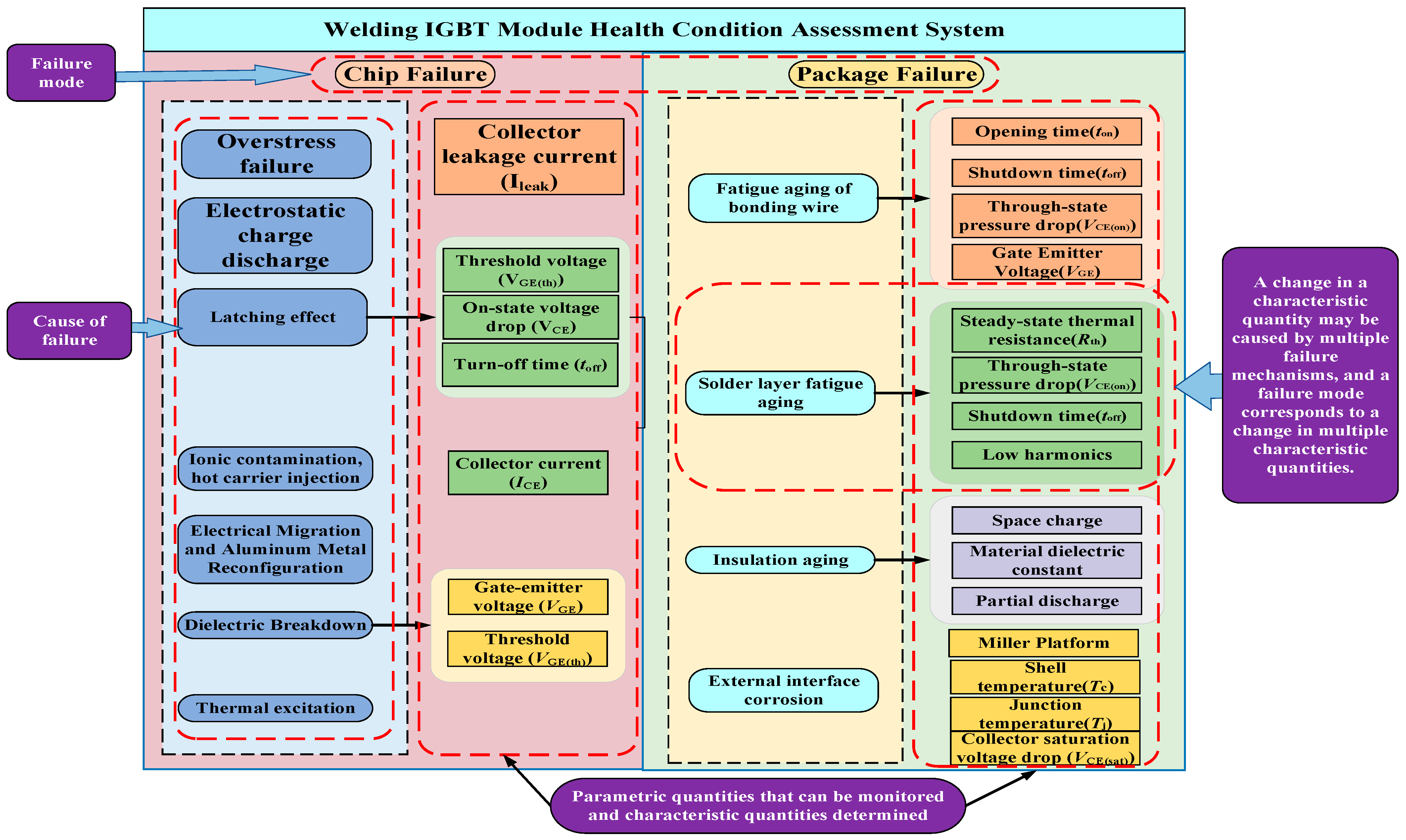
2.2.2. IGBT Module Failure Mechanisms

IGBT module failure modes are mainly categorized into chip-level failure and package-level failure [29]. The main failure causes, and modes are shown in Figure 3. Generally, overstress will cause IGBT chip failure. Package failure is caused by multiple factors and is closely related to the internal structure. Common failure modes are bond wire failure and solder layer aging [30].
1
IGBT module chip failure mechanism;
Overstress failure: Studies have shown that electrical overstress failures are generally associated with overcurrent and overvoltage, and thermal effects and secondary breakdown generated by high voltage are the main failure problems [31]. Therefore, the thermal system of IGBT modules should be strictly designed to ensure that the IGBT modules work in a safe working area. At the same time, IGBT modules should have a certain tolerance to overcurrent, and the relationship between the number of module overcurrent and failures has been studied in the literature [32], which has the potential to realize condition monitoring and evaluation based on overcurrent detection and early warning for IGBTs. Under the action of overcurrent stress, hot spots are formed locally in the IGBT devices. When the local temperature is too high, it can cause the device to crack and then fail.
Electrostatic charge–discharge: The electrostatic discharge may break through the local gate oxide layer. If the operator works with static electricity in hand, the instantaneous high voltage value may break through the local gate oxide layer of the IGBT module. Although the module can still work normally, this has already caused damage to the module, and such defects are not easy to find. When a higher voltage is encountered again, it may lead to a gate short circuit and failure. Local gate failure can be detected by measuring the gate charging time constant [33]. In practical engineering applications, the failure of IGBT modules caused by electrostatic discharge is frequent and difficult to avoid.
Latch-up effect and parasitic transistor conduction: The latch-up effect is due to the presence of parasitic inductance inside the module, the IGBT can not be shut down properly, and the IC increases rapidly, which ultimately leads to chip failure.
The excessive rate of voltage change during the turn-off process of an IGBT module may induce a short circuit owing to the conduction of parasitic transistors inside the IGBT chip [34]. Although this problem can be significantly improved by optimizing the layout of the semiconductor module, monitoring the value of the maximum voltage variation rate is still important to avoid latch-up effects.
Ionic contamination, hot carrier injection: Ion contamination is caused by the accumulation of ions at high field strengths resulting in electric field distortion, while hot carrier injection is caused by the growth of defects in the gate oxide layer. At high temperatures, hot carriers are injected into the gate oxide layer when the carrier energy exceeds the lattice potential barrier, causing damage [35]. IGBT is a semiconductor device based on a gate MOS structure, and its gate oxide layer is thicker than the MOSFET. Gate damage caused by hot carrier injection is less common, but it will lead to changes in the external characteristics of IGBT, such as gate threshold voltage, transconductance, and leakage current, eventually leading to device failure.
Electrical migration and aluminum metal reconfiguration: Because of the aging of IGBTs during long-term power cycling, the electric field on the surface of IGBT chips becomes uneven, and under the action of electric potential, aluminum atoms will migrate. During the long-term power cycling of IGBT modules, the aluminum metal plated on the silicon surface may also melt and condense due to temperature fluctuations; that is, the reconstruction phenomenon occurs. The aluminum metal surface of the new device chip is very flat and regular, while the aluminum metal surface of the aged device chip is very rough and irregular, which leads to an increase in surface resistance [36], which increases the on-resistance of the IGBT module and indirectly increases the on-voltage drop of the IGBT. Under a certain current, the power loss of the module will increase, and the junction temperature will also increase, which is not conducive to the reliable operation of the IGBT module.
Thermal excitation: The main manifestation of thermal excitation is damage to the chip’s internal wafer owing to the high temperature in the local area of the chip, which is very closely related to the junction temperature. According to Arrenius’ law [37], the thermal excitation process intensifies when the junction temperature of the chip increases, thus accelerating chip failure.
Cosmic ray radiation: In normal use, devices are subject to external radiation, and when energetic particles from space pass through a semiconductor device, their collision with silicon atoms produces plasma gases generating current pulses that may cause the chip to fail.
2
IGBT Package Aging Failure Mechanisms;
As shown in Figure 1, the IGBT module package structure was designed and manufactured using a variety of material combinations, and the realization of its complete electrical function directly depends on the integrity of the structure. However, there is a mismatch of force and thermal properties between IGBT module materials during long-term operation, the internal material performance of the device is degraded, and the structural integrity of the device is destroyed owing to environmental factors or fluctuation of the device’s working conditions, which eventually leads to package failure of the IGBT module.
Bonding line fatigue: The bonding wire was bonded to the chip and the copper layer on the DBC using ultrasonic bonding technology. The electrical connection between the chip and chip, chip and external electrical terminals was made using bonding wires made of aluminum or aluminum alloy. In an IGBT module package structure, bonding wires are usually placed in parallel to improve the current transmission capability of the module. The physical bonding line in the IGBT module is shown in Figure 4. In practice, the forward conduction current flowing through a controllable device causes the temperature to rise, while in reverse conduction, it causes the temperature to fall, so the power module is constantly subjected to temperature changes. Since the materials of the chip and the bonding line are different, the coefficients of thermal expansion of the materials are naturally different, and shear stresses are generated at the bonding point under constant temperature impact. Under the effect of shear stresses generated by temperature fluctuations, this will produce fine marks at the surface or heel of the bond wire [38] and will gradually deepen over time, eventually causing the bond wire to peel and fracture [39]. In this case, the thermomechanical stress εT generated at the bond can be expressed by Equation (2) [40].
ε T = ε 0 + ( α A L α S i ) ( T j T c a s e )
ε0 is the thermomechanical stress generated under normal operating conditions; α is the coefficient of thermal expansion of different materials; Tj is the junction temperature of the IGBT chip; Tcase is the temperature of the aluminum bonding line at the initial moment.
During the normal operation of an IGBT module, we should always pay attention to the change in the chip junction temperature and control the fluctuation of the junction temperature within a reasonable range. In the process of chip manufacturing and material selection, materials with small differences in the thermal expansion coefficient should be selected to reduce the chance of plastic deformation of the aluminum bonding line and improve the service life of the chip. As the aging of the IGBT module bonding line increases, the number of broken or detached bonding lines increases with aging time, resulting in greater electrical stress on the remaining bonding lines. This eventually aggravates the aging process of the remaining bonding lines and accelerates the aging failure of the IGBT module.
Solder layer fatigue: The solder-type IGBT module consists of two parts: a chip solder layer and a substrate solder layer. Owing to the diversity of packaging materials, the thermal expansion coefficients between layers are different. During operation, owing to constant temperature fluctuations, different thermal stresses are generated on the surface of different layers, which in turn leads to different degrees of deformation in each layer of the material. Compared to the other layer, the solder is thinner and has a lower modulus of elasticity; thermal, the solder layer is subjected to most of the thermal stresses under the same thermal stress conditions and is, therefore, more susceptible to fatigue failure. Under thermal stress, the solder layer will gradually develop cracks and voids [41], and eventually, solder layer delamination occurs. Figure 4 shows a physical image of fatigue failure of the IGBT solder layer observed by scanning electron microscopy (SEM) [42]. In this case, the generated thermoelectric stress Fs at each solder layer can be expressed by Equation (3).
F S = L Δ α Δ T S 2 H S
where L is the length of the IGBT chip, ∆α is the difference in coefficient of thermal expansion between adjacent layers (chip layer, DBC layer, DBC layer, and copper layer), ∆TS is the amount of change in the temperature of the solder layer (chip solder layer or DBC solder layer), and HS is the thickness of the solder layer. From Equation (3), it can be seen that the thermoelectric stress generated at the solder layer is inversely proportional to the thickness of the solder layer, proportional to the difference in the coefficient of thermal expansion between adjacent layers, and proportional to the amount of change in the temperature of the solder layer. That is, the greater the difference in the coefficient of thermal expansion, the greater the change in temperature at the solder layer, and the greater the thermoelectric stress generated at the solder layer, the more likely it is that the solder layer will undergo fatigue aging.
In addition, fluctuations in the ambient temperature can cause cracking and lead to failure. Typically, solder layer fatigue is most affected by temperature, while other factors, such as corrosive environments and vibration, also affect the degree of material deformation [42], as shown in Figure 5. Although other factors are not as influential as the temperature, the interaction between multiple factors accelerates the fatigue aging process of the solder layer.
External interface corrosion: In high-humidity and high-salt spray environments, external interface corrosion is a failure mode that cannot be ignored. The metal interface exposed to a high salt spray and high humidity is the weakest link of the module, and its corrosion phenomenon can directly affect the electrical characteristics of the module. The manner in which corrosion occurs is highly dependent on the materials involved and the presence of contaminants. Moisture in the package and high electric fields can lead to the migration of ionic substances, a phenomenon that is well-explained by the electrochemical migration of metals [43]. Typical examples include the corrosion of copper wires and contact points. Chlorine contamination and water can greatly accelerate chemical reactions in this process [44]. Crevice corrosion owing to hydrolysis is also an important chemical reaction that occurs at the module interface, which reduces the effective contact area at the interface and consequently increases the contact resistance at the interface. The initiation site of metal corrosion is related to the defects in these layers. These weak spots are caused by the heterogeneity of the microstructure and may lead to localized corrosion of the metal [45]. When biased from the outside, the adsorbed water was hydrolyzed, resulting in a large pH distribution between the biased electrodes. At the anode, H+ ions accumulate, shifting the properties of the solution to the acidic range, whereas a more alkaline environment is established at the cathode because of the accumulation of OH ions. Once corrosion begins, the rate of metal dissolution in the corrosion cell is primarily controlled by the applied voltage. The potential difference acts as a driving force and, therefore, has an important influence on the corrosion reaction and its consequences. Furthermore, ionic contaminants can significantly accelerate the process even in the absence of a potential difference, resulting in a unique corrosion mechanism. Furthermore, the literature [45] shows that the corresponding high-temperature stress tests without humidity and salt spray do not exhibit any anomalies, which is a good indication of the importance of considering humidity and salt spray.
Insulation material aging: It was shown that partial discharges in the pores at the interface between the ceramic and metal layers produced small discharge amplitudes, as shown in Figure 6, while the partial discharges at the metal edges were in the range of a few nC, leading to the decomposition of silica gel into gaseous products and reducing the insulating capability of the material [46]. It was shown that partial discharges and dendrites caused by metal protrusions in silica gel-encapsulated insulation found that silica gel showed limited self-healing ability at pulsed voltages and was effective only for isolated, non-repetitive partial discharges, while the insulation properties could not be recovered after a series of partial discharges [47].
Compared to elastic silicone gel-encapsulated insulation, epoxy resin has a high Young’s modulus but is susceptible to mechanical failures, such as cracking during cold and thermal cycles. It was found that, experimentally, air-gap partial discharges are prone to occur at tiny bubbles inside the epoxy resin, and the oxygen content at the interface increases significantly after the discharge [48]. The effect of pulse rise time on the electrical tree initiation and growth characteristics of epoxy resin was investigated (Figure 7). The results show that compared with the conventional sinusoidal voltage, the pulse-width modulated voltage increases the probability of electric tree initiation and growth rate. At a certain temperature, as the rise time decreases, the probability of electric tree initiation increases, the growth rate of the electric tree increases, and the morphology of the electric tree gradually evolves from dendritic to jungle-like [49]. Therefore, when choosing epoxy resins as encapsulation materials for power electronics, the pulse-width modulated voltage rise time, carrier frequency, and thermal effects on insulation performance should be fully considered [50].
In addition, the insulation structure consisting of substrate metal electrodes, substrate ceramic insulation, and potting insulation together tends to combine at the point where the local electric field is concentrated, and at the same time, the starting discharge voltage of partial discharges is reduced due to the introduction of voids, etc., into the module during the manufacturing process.

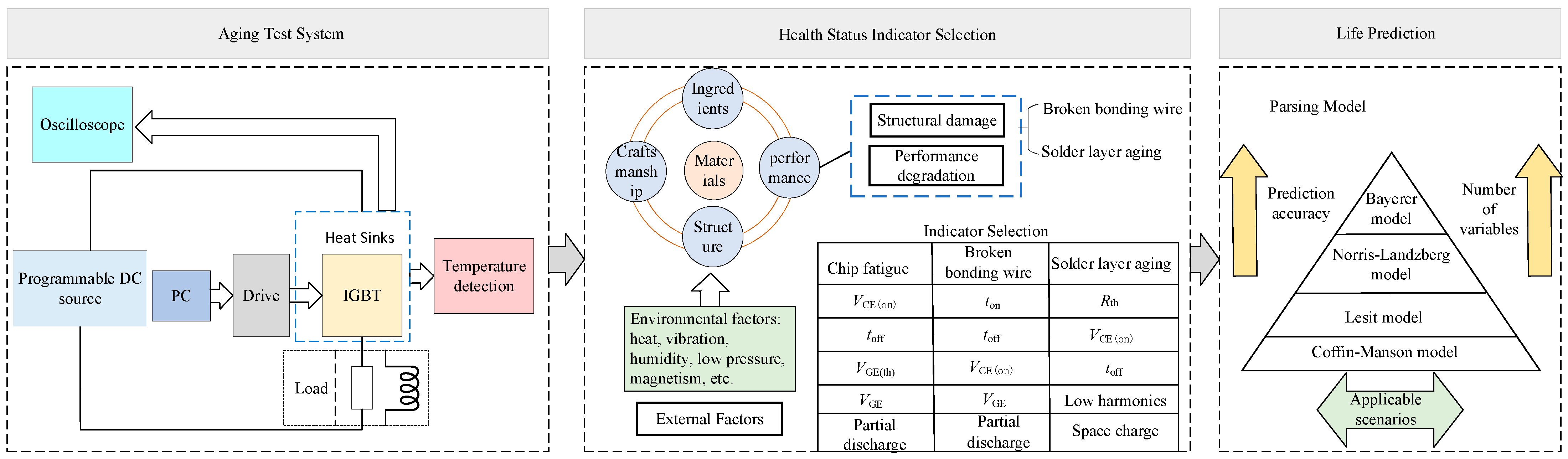
3. IGBT Module Health Status Monitoring Method

Condition monitoring refers to the use of various detection and analysis methods to monitor various parameters that reflect changes in the operating status of the device in order to determine whether the device is working in a normal state and for abnormal conditions, to track and predict its development trend in order to determine what countermeasures to take. The main purpose of condition monitoring is to prevent the occurrence of faults, reduce losses, and improve device utilization. Research in this area is discussed and summarized by classifying the types of faults that are monitored.

3.1. Sensor-Based Condition Monitoring Method

The junction temperature of IGBT modules is mainly measured directly by high-cost devices, such as infrared thermal imaging cameras, optical fibers, infrared radiation sensors, and infrared microscopes, which require tools to open the package structure of IGBT power modules, remove the silicone inside the package, and blacken the chip surface to increase its thermal radiation coefficient to improve the accuracy of junction temperature extraction measurements. Because most of these devices are expensive, there is a gap between the sampling rate and the monitoring requirements, and the method will destroy the integrity of the module, and it is generally only used for junction temperature extraction of semi-finished devices.

3.1.1. Infrared Detection Method

The infrared thermal imaging method uses an infrared thermal imager to capture a high-speed camera of the IGBT module [51] and calculates the temperature value of each point of the module based on the color in the image to derive the two-dimensional temperature distribution of the IGBT module. This method is a non-contact measurement of junction temperature, which can accurately measure the rapid change of junction temperature and chip temperature field distribution. However, it also needs to destroy the module package structure and remove the silica gel on the surface of the absolute chip, which affects the actual temperature distribution, which has a certain error and is only applicable to laboratory conditions.

3.1.2. Eddy Current Pulse Thermography ECPT

Eddy current pulse thermography ECPT is a non-destructive condition monitoring method that does not require contact with the inspected sample. The method uses a magnetic field as the excitation source to inductively heat the conductive material by eddy currents, records thermal video of the module heating with an infrared camera, and finally transmits the video data to a PC for visual post-processing to identify defects. Although eddy current pulse thermal imaging ECPT can achieve nondestructive monitoring of single bonding line defects in IGBT modules, the method requires a special set of equipment, which makes it difficult to integrate the method into converters. Compared to other monitoring methods, this method requires a longer monitoring time, making it difficult to achieve real-time online monitoring. This method can be used in the laboratory, and its application in industrial practice requires further study.

3.1.3. Thermal Sensor Method

It refers to the temperature measurement using a thermocouple, temperature-sensitive resistor, and fiber optic probe to directly contact the surface of the IGBT module chip. This method can be used to directly obtain the junction temperature and is simple to test. However, temperature measurement using thermocouples, thermistors, and optical fibers requires opening the module package, slow thermal response time, and covering the surface of the IGBT chip with bonding lines, which makes it difficult to place thermal components, all of which affect the measurement accuracy [52].

3.2. Model-Based Condition Monitoring Method

By establishing thermal network models, the Foster and Cauer models became dominant. These thermal network models need to know the material properties, geometric structure, and physical properties of each layer of the device when they are established and represent each layer with the corresponding RC network. The temperature at different positions of the module to be measured can be obtained according to the positions of the different nodes in the thermal network. Therefore, this method requires a high level of knowledge of the internal structure of the power device and the material properties of each layer. In the literature [53], the thermal network model of an IGBT is proposed to measure the junction temperature online, and the calculation formula is shown in Equation (4); Tc is the shell temperature, which can be measured directly by the temperature sensor; Zthj-c(t) represents the thermal network model of the IGBT module from junction to shell; and Ploss represents the power loss of the IGBT module.
T j ( t ) = T c ( t ) + P l o s s × Z t h j c ( t )
The advantage of the model-based state monitoring method is that it does not need to disassemble the module for measurement, it does not use any additional equipment, and it can measure the junction temperature only by mathematical calculation, which can realize online measurement. The disadvantage is that there are anti-parallel diodes inside the IGBT module in addition to the IGBT chips, and the high-power module has half-bridge, full-bridge, three-phase bridge, and other package forms. Each IGBT chip is connected to the module substrate, the IGBT module thermal coupling occurs between the chips during operation, and the thermal coupling parameters are difficult to obtain [54]. In addition, after aging the solder layer of the IGBT module, the thermal network parameters change, and the junction temperature calculation with the original thermal parameters generates large errors.

3.3. Condition Monitoring Method Based on Surface End Characteristics

Failure of an IGBT module may lead to changes in its internal structure, which affects the output characteristics of the device. As the number of power cycles increases, thermomechanical stresses fatigue the solder layer and cause buckling, resulting in a gradual increase in the IGBT through-state voltage drop. Aging of the solder layer also causes an increase in thermal resistance and power loss inside the module, leading to an increase in the chip junction temperature [55]. The literature [56,57,58] investigated the characteristics of the IGBT on-state voltage drop, cross-conductance, and gate threshold voltage with temperature before and after fatigue by means of electrothermal loading experiments.
The literature [59] samples the IGBT on-state voltage and current in a smart power module. For a certain current measurement, a lookup table can be used to find the corresponding normal on-state voltage value and compare it with the measured value, and their deviation can reflect the internal lead failure of the module. However, in practice, accurate online measurement of the IGBT pass-state voltage is difficult owing to measurement errors, weak signal variations, temperature variations, and electrical isolation, which limit the engineering applications of these methods. The literature [60] analyzed the dynamic characteristics of IGBTs in several operating states and pointed out that the main cause of IGBT failure is the change in internal physical parameters and even structure due to the long-term thermal shock of the device. It has been pointed out that the accumulation of internal damage caused by thermal stress will lead to a decrease in the Miller capacitance and, thus, the degradation of the gate voltage Miller platform. However, the simulation and experimental results show that the change in the Miller platform due to the lead shedding is very small, and it may be difficult to achieve accurate measurements in the actual system if the measurement error is considered. It has been proposed in the literature that the condition monitoring of IGBT modules can be achieved by continuous measurement of the relevant electrical parameters at the device ends. There are other methods to monitor other end characteristics of IGBT modules and use the monitored data to compare with the value at the normal point state of the point to determine whether the device is failing.
The advantages and disadvantages of various monitoring methods are summarized according to the failure modes of IGBT modules, as shown in Table 1. In summary, monitoring the junction temperature by physical contact methods, such as fiber optic probing, can generate a one-dimensional thermal load file, whereas two-dimensional thermal loads can be obtained by infrared thermography. Both methods require opening the package and are affected by the thermal response delay time of the measurement equipment; therefore, there is a certain measurement error, which is suitable for experimental verification of junction temperature prediction. The temperature-sensitive parameter method is more accurate and does not need to destroy the package, which is suitable for engineering applications. However, it requires the selection of applicable heat-sensitive electrical parameters according to the characteristics of the power device to ensure the accuracy of the test.

4. IGBT Module Condition Monitoring Health Indicators

IGBT module aging failure on system reliability, health state monitoring can effectively improve the reliability of the module. According to the size of the deviation between the module’s actual state characteristic quantity and the normal state characteristic quantity, the aging degree of the module to realize the identification and tracking of module failure precursors can be determined.

4.1. State Eigenvolume Based on Voltage Parameters

4.1.1. Saturation Pressure Drop

IGBT devices operate in the saturation region driven by the gate voltage. Because they are not ideal switching devices, the voltage difference between the collector and emitter of the IGBT is not zero, and there is a certain voltage drop, which is called the IGBT saturation voltage drop. Studies have shown that, in experiments conducted to accelerate the aging of IGBT power modules, the saturation voltage drop Vce(sat) gradually increases with the failure process. In engineering studies, it is usually considered that an IGBT module fails when the saturation voltage drop value rises above 5% of the normal value [61,62].
The IGBT saturation voltage Vce comprises the chip voltage Vce-chip and package voltage Vce-packpage. The chip voltage Vce-chip, in turn, consists of the voltage applied to the PNP part as well as to the MOSFET and is (5):
{ V c e c h i p = V P N P + V M O S V P N P = 2 k T q ln [ I C W N 4 q D n n i p Z f ( W N 2 L a ) ] V M O S = I C L C H Z μ n i C o x ( V G V t h )
where k is the Boltzmann constant, T is the absolute temperature, q is the charge of the electron, WN is the width of the n-type drift region, Da is the bipolar diffusion coefficient, ni is the intrinsic carrier concentration, p is the cell pitch, Z is the cell width in the direction perpendicular to the cross-section, LCH is the channel length, μni is the electron mobility of the anti-type layer, Cox is the unit capacitance of the gate oxide layer, VG is the gate bias voltage, and Vth is the threshold voltage.
The relationship between the IGBT on-state voltage, junction temperature, and current was analyzed by V. Smet et al. [63]. The effects of the temperature and current on the state voltage drop were considered. An online monitoring circuit and a method based on different-state voltage drops were proposed. It was shown that there is an approximately linear relationship between junction temperature and on-state voltage drop; Li Yaping et al. proposed a bonding damage state monitoring method based on collector saturation voltage drop to characterize bonding damage by saturation voltage drop at specific collector current with zero temperature-sensitive characteristics [11], which avoids the influence of junction temperature on saturation voltage drop measurement, but the collector current is time-varying under variable current conditions, and the monitoring conditions cannot be guaranteed [64,65]; Chongqing University’s Wei Lai et al. studied the aging failure mechanism of IGBT by power cycle test, obtained the on-state voltage drop of the device during the power cycle in real-time, obtained the conclusion that the on-state voltage drop increases with the deterioration of the device state, and gave a specific threshold value to judge the failure form of device bond line breakage [66]. In summary, it can be seen that the main influencing factors of Vce-chip are junction temperature Tj and collector current Ic. Figure 8 shows the output characteristic curves of the IGBT modules at different temperatures. The saturation voltage is not temperature sensitive when the current value is at the intersection point, which is called Vce-int. When the collector current is larger or smaller than the intersection point, the saturation voltage exhibits opposite temperature sensitivity. Therefore, the conventional mathematical function model cannot accurately describe the nonlinear mapping relationship, resulting in a large error in the final estimated junction temperature. In actual operating conditions, IGBT modules generally operate under high-power and high-current conditions; therefore, it is difficult to apply this method to the operating conditions.

4.1.2. Gate Voltage

As the gate input capacitance of high-power multi-chip IGBT modules decreases with module chip branch defects, it affects the circuit response of the gate input loop. To avoid the influence of the power measurement voltage and current of the multi-chip IGBT module on the turn-on process, ref. [67] proposes the use of the gate voltage of the module that has not reached the threshold voltage, that is, the pre-threshold voltage gate signal VGE(pre-th), to characterize the state of the multi-chip IGBT module owing to the chip branch defect caused by the failure of the bonding line, and obtain the state characteristic quantity VGE(pre-th) by delayed sampling. Chip branch defects were simulated by cutting the bonding line.
However, VGE(pre-th) is the switching transient quantity of the IGBT module, which not only has high requirements for signal acquisition but also does not easily eliminate the possible noise problem in the switching [68]. This method requires a fixed delay to achieve acquisition, which imposes strict requirements on timing control. In addition, the junction temperature has an effect on the VGE(pre-th). These problems limit the practicality of this monitoring method. The method is applicable to the monitoring of chip branch defects in multi-chip IGBT modules and is not applicable to the monitoring of defects in single-chip modules or single bonding lines [69]. In addition, signals are used during part of the module switching process and combined with algorithms to identify the chip branch defect status. Yang Yanyong et al. tested the dependence on the bus voltage, load current, and junction temperature by testing the on-gate voltage overshoot and proposed that the on-gate voltage overshoot-based method has high sensitivity in identifying weld line faults at the initial stage, and the gate on voltage overshoot of IGBTs increases with the severity of bondline faults [59]. The literature [70] showed that the Miller plateau time tGP of the shutdown process also effectively reflects the degree of IGBT bondline aging, and its value has a significant decreasing trend with an increase in bondline aging, which can be used as an effective characteristic parameter for condition monitoring. At this stage, voltage Vge is maintained at a fixed value and does not change. Both the duration of the Miller plateau and the voltage value are directly related to the Miller capacitance Cgc, which is calculated by Equation (6):
C g c = C o x d C d e p C o x d + C d e p = C o x A a i C d e p C o x A a i + C d e p
where Cox is the oxide capacitance per unit area, ai is the ratio of the IGBT chip inner cell to the entire pad area, Aai denotes the area of the inner cell within the IGBT chip pad, and Cdep is the depletion layer capacitance. For partially failed IGBT modules, the dislodgement of bonding leads to a reduction in the effective contact area of the structural capacitance; thus, the Cgc of the failed module will be reduced, and the duration of the gate drive voltage Miller plateau will be shortened.
Junction temperature fluctuations also have an impact on the Miller plateau time of the turn-off process, and the junction temperature must be kept the same during monitoring. For partially failed IGBT modules, dislodged bonding reduces the effective contact area of the structural capacitors, and the Miller plateau duration of the gate drive voltage is shortened. By using algorithms such as wavelet analysis theory, time series, and power spectral density-based algorithms to identify the state of chip branch defects in multi-chip IGBT modules due to bonding lead failure, the noise suppression capability of the monitoring results can be improved, or the discrimination effect can be increased to a certain extent. However, the acquisition and storage of switching gate voltages are still difficult in the implementation of condition monitoring, which limits the application of these methods.
IGBT devices are voltage-controlled components that operate by applying a certain positive bias voltage VG to their gates, and the gate voltage should be greater than the threshold voltage. This is due to the fact that when the performance of IGBT devices decreases due to aging, the internal gate oxide layer will be changed, thus causing the gate capacitance parameters to change. As a result, the aging failure of IGBT devices causes the gate threshold voltage VGE(th) to increase relative to the initial state, and there is a correlation between it and the failure process, which can be used as a state characteristic parameter to monitor the aging failure state of IGBTs.

4.2. State Characteristic Quantities Based on Current Parameters

4.2.1. Gate Peak Current Igpeak

Igpeak is the peak gate drive current caused by the inductive load and continuity diode during the on-state delay to the on-state of the IGBT power module. The quantitative relationship between bondline aging and Igpeak was obtained in the literature [71] by establishing the voltage differential equations for different states of the IGBT power module as shown in Equation (7), where Vgeon and Vgeoff are the turn-on and turn-off voltages provided by the gate drive, respectively; Rg is the gate equivalent resistance, which is expressed as shown in Equation (8) and contains the external gate resistor Rgin, the As the bonding line and solder layer age Rpara increases, resulting in a decrease in Igpeak.
I g p e a k = V g e o n V g e o f f R g
R g = R g i n + R g e x + R p a r a

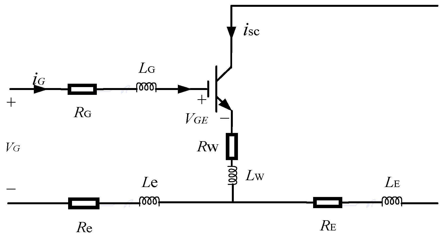
4.2.2. Short-Circuit Current Isc

When the IGBT module is short-circuited, it operates in the current-active region. At this time, its internal equivalent circuit is shown in Figure 9.
Where iG is the gate drive current, isc is the short-circuit current, VG is the gate drive voltage, and VGE is the chip-level gate-emitter voltage of the IGBT module.
When the gate drive voltage is stabilized, the steady-state value of the short-circuit current of the IGBT module, Isc, is related to the gate drive voltage, VGE, as shown in Equation (9) [72]:
I S C = μ n i C O X Z 2 L C H ( 1 α P N P ) ( V G E V T H ) 2
where Cox is the oxide layer capacitance, Z is the channel width, LCH is the channel length, which is determined by the chip structure and is not affected by the operating environment, ni is the electron mobility, αPNP is the common base amplification of the PNP transistor, VTH is the gate threshold voltage. All these parameters are affected by the junction temperature.
When the IGBT module short-circuit process enters a steady state, the gate drive current iG and its rate of change are 0, the short-circuit current isc is the steady-state value ISC, and its rate of change is 0. Then, the IGBT chip-level gate emitter voltage can be simplified as
V G E = V G R W I S C
Substituting (10) into the above equation yields
I S C = μ n i C O X z 2 L C H ( 1 α P N P ) ( V G R W I S C V T H ) 2
As can be seen from Equation (11), the magnitude of the short-circuit current in the short-circuit steady-state case of the IGBT module is affected not only by the junction temperature but also by the equivalent resistance of the bonding lines in the package structure.
The transfer characteristic curves of the IGBT module are shown in Figure 10, which shows the relationship between the gate drive voltage and collector current in the active operating region. When the gate drive voltage is VGT at the intersection of the transfer characteristic curves at different temperatures, the effect of the junction temperature of the IGBT module on the short-circuit current can be neglected. That is, the short-circuit current at a specific gate drive voltage (VGT) is only influenced by the equivalent resistance of the bonding line, and ISC monotonically decreases with respect to RW according to the analysis of Equation (11). Therefore, the aging of IGBT module bonding wires can be monitored by monitoring the short-circuit current value at a specific gate drive voltage (VGT), which provides a theoretical basis for using the short-circuit current as a characteristic quantity of IGBT module bonding wire aging.

4.2.3. Leakage Current

The collector–emitter leakage current was found by Zhang Chinghao et al. to be an indicator that can reflect the degree of aging of the silicon material of IGBT chips and can be expressed as
I l e a k = I l e a k ( D ) + I l e a k ( S C ) + I l e a k ( e m )
The parameters on the right side of the equation are the diffusion zone leakage current, space charge zone leakage current, and emitter interface leakage current, in that order. When degradation of the silicon base material occurs, the emitter interface of the IGBT tends to form hot spots and accelerate the interpenetration between silicon and aluminum atoms at the interface, and the emitter interface leakage current increases. Studies have shown that the emitter interface leakage current is nearly zero in healthy IGBTs but increases linearly with the degree of silicon degradation (θ). By conducting constant temperature and pressure accelerated aging tests and accelerated thermal cycling experiments, it was found that the collector–emitter leakage current as an IGBT module chip aging monitoring index increases linearly with the degree of IGBT module chip degradation. However, there are relatively few studies on this method, and the influence of measurement error on the monitoring results needs to be further examined.

4.3. State Characteristic Quantities Based on Temperature Parameters

4.3.1. Junction Temperature

Among the various types of failure factors, about 55% of power electronic system failures are mainly induced by temperature factors [73]. Li Jie and Lai Wei et al. characterized the module junction temperature based on the change of temperature-sensitive electrical parameters, which has a high response speed, and the results show that with the shedding of the solder layer, the IGBT junction temperature and shell temperature increase significantly, and the temperature fluctuation becomes larger [10]. Therefore, online monitoring of the junction temperature is the basis for the health status assessment of IGBT modules.
Current types of junction temperature monitoring are optical measurements, physical contact methods, temperature-sensitive parameter methods, and analytical methods [74]. Among them, physical contact measurement uses temperature-sensing elements such as thermistors or thermocouples for testing, which can only measure the average temperature outside the device, making it difficult to achieve online monitoring of the junction temperature. Optical non-contact measurements are damaging to the device itself and are not suitable for online junction temperature monitoring.
The power loss of the device includes through-state loss and switching losses. The thermal path network is divided into the Foster model and the Cauer model, which can be obtained by transient thermal impedance curve fitting, and the Cauer model requires access to specific physical parameters of materials in the IGBT structure, which is more difficult to implement [75]. The thermal path network is key to obtaining the junction temperature using the thermal path model method. The accurate establishment of a thermal path network lies in the accurate acquisition of the transient thermal impedance curve of the device. The transient thermal impedance can be calculated experimentally by obtaining the heating or cooling curves of the device. It is also possible to establish a finite element simulation model and obtain it using a step response calculation, given a known power loss. Based on the linear relationship between damage and thermal resistance in the aging process of IGBT devices, Chen Min-uran et al. of Chongqing University calculated the device cumulative damage using the change of junction temperature in the thermal load curve and increased the thermal resistance in the Foster thermal network by 10% for every 20% increase in cumulative damage to obtain more accurate junction temperature information during device aging [76]. Zhen Hu et al. used the IGBT substrate temperature gradient as an indicator of solder layer aging; when the thermocouple is monitored, there is a change in the temperature gradient, and the true thermal resistance was calculated based on the linear change law of thermal resistance to update the thermal network. Moreover, the junction temperature error of the device calculated using this method was significantly reduced [77].

4.3.2. Internal Thermal Resistance

The difference between the junction temperature and shell temperature and the power loss is defined as the steady-state thermal resistance. As the IGBT module works for a long time under the influence of temperature fluctuation stress, each material is subjected to different shear forces resulting in the solder layer being prone to cavities and cracks, which makes the steady state thermal resistance increase continuously and ultimately causes the device aging failure. As the aging process continues to develop, it is likely to lead to catastrophic failures such as a secondary breakdown. Therefore, the thermal resistance Rth of IGBT modules can be used as a state characteristic parameter to monitor and evaluate its aging failure state.
Xiang and Li Ran et al. studied a 20% increase in the steady-state thermal resistance Rth as an indicator of severe failure of the solder layer of IGBT devices [16]. Thermal resistance is defined as the temperature between two closed isothermal surfaces divided by the total heat flow between them. In IGBT power modules, the two isothermal surfaces are the connection point Tj and the case Tc, and the total heat flow between them that is, the conduction loss, is Pon. The mathematical definition of thermal resistance can be expressed as
T j = T c + P o n × R t h
R t h = T j T c P o n
where Pon is the power loss of the IGBT in the on state, which is obtained by the product of the collector current Ic and the saturation voltage drop VCE. The case temperature Tc can be measured by installing a specific temperature sensor at the bottom of the module, whereas the junction temperature Tj needs to be measured by intruding into the module. This method can grasp the working operation of the IGBT power module without interrupting the normal operation of the IGBT module and realizing online monitoring; however, it also has obvious shortcomings; first, the measurement of the shell temperature Tc requires high stability and accuracy of the temperature sensor used for measurement; second, the measurement of the junction temperature Tj is invasive, and the accuracy of the measurement is also affected by the installation position of the sensor; and finally it is necessary to establish a high-precision electrical, thermal model to calculate the thermal resistance [78]. However, it is usually more difficult to establish a high-precision electrical, thermal model, which needs to consider the heat generation power loss and remove the influence of the ambient temperature.

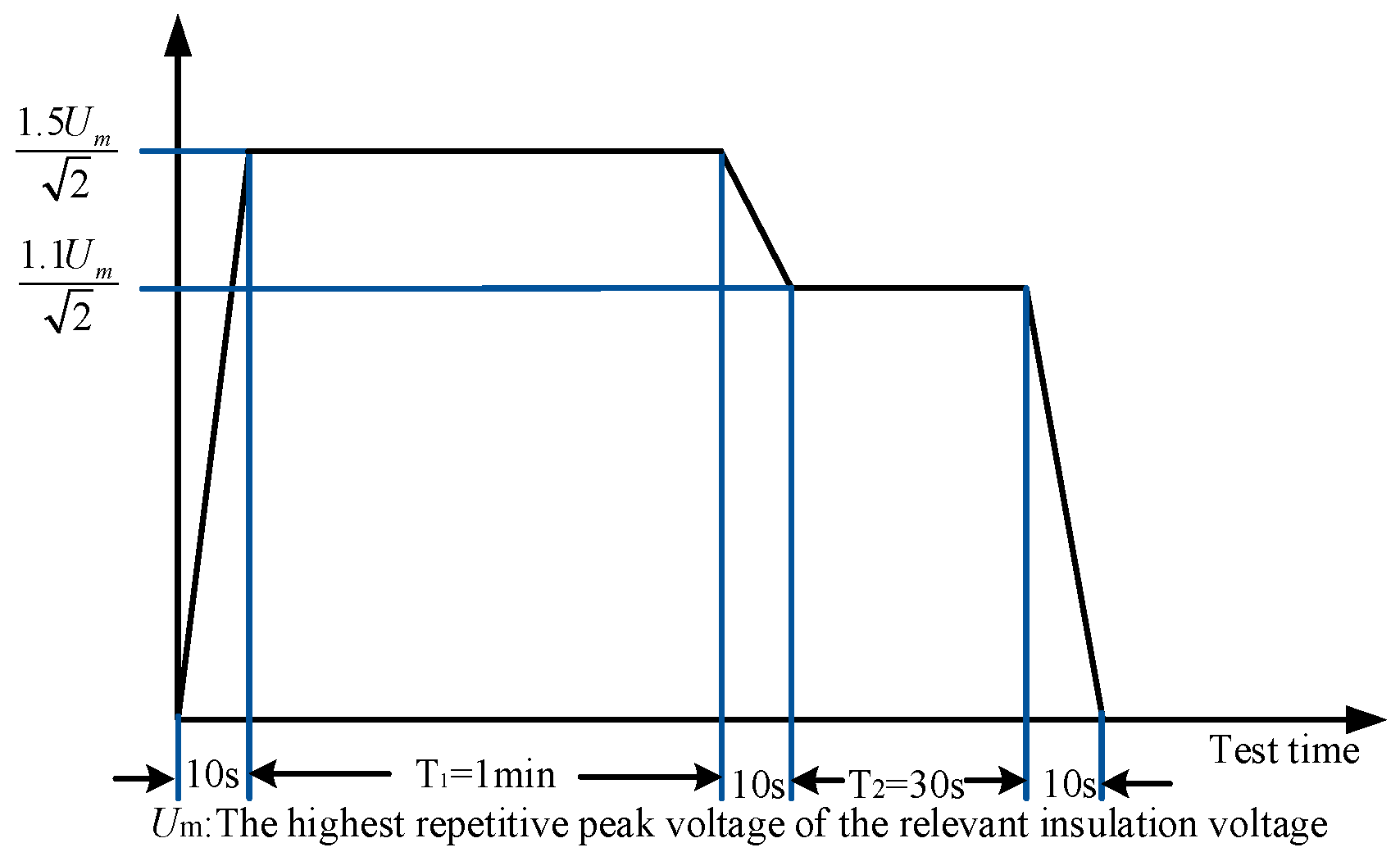
4.4. State Characteristic Quantities Based on Insulation Parameters

With the gradual increase in the device operating voltage, the requirements for the withstand voltage of IGBT power devices are increasing; therefore, the insulation of IGBTs is a prominent issue [79]. There have been good results from dielectric response tests to the study of evaluating the insulation performance of IGBT modules using partial discharge detection.

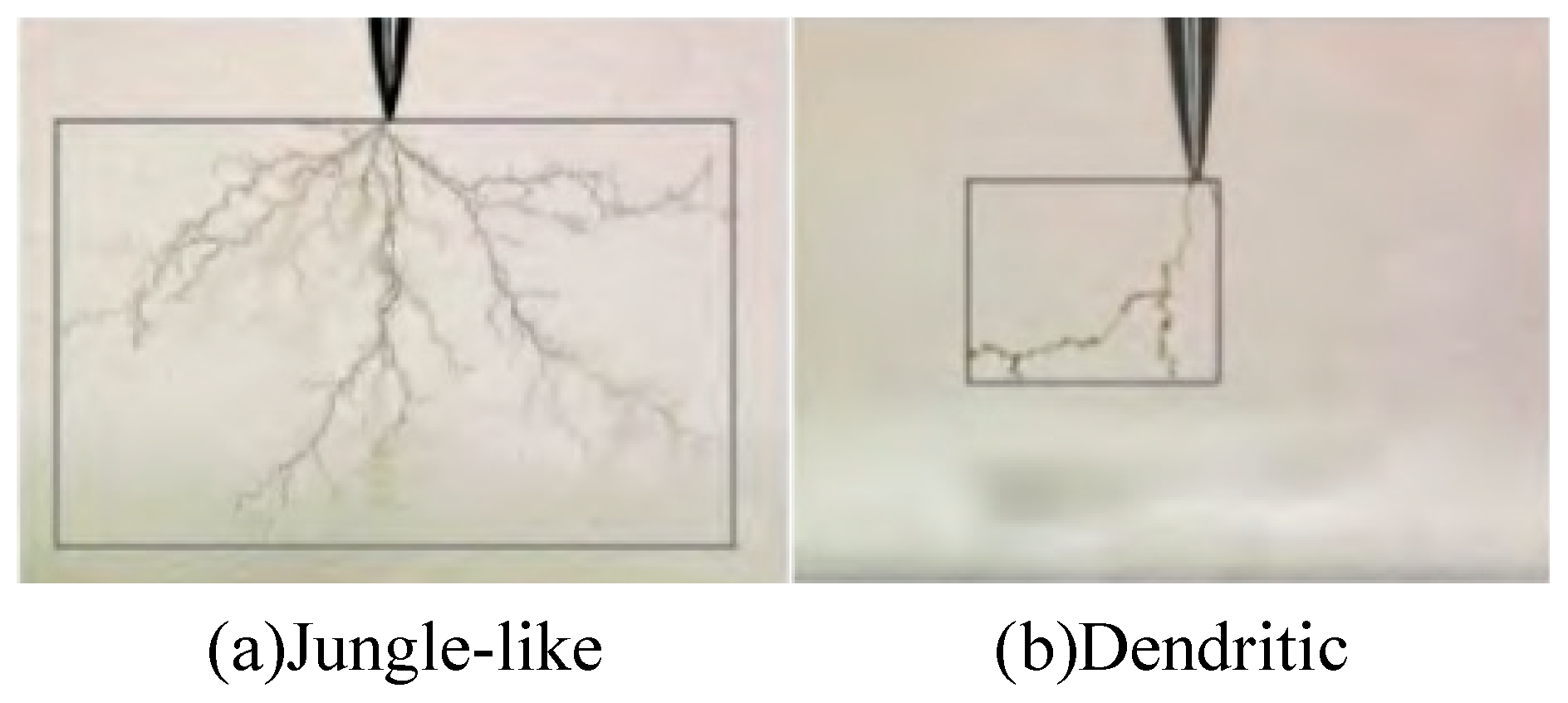
4.4.1. Dielectric Response

Arumugam et al. obtained the broadband dielectric response spectra of solder-type IGBT modules under different aging states and found that the information of device capacitance and dielectric loss spectra in the frequency band from 0.1 Hz to 1000 Hz can reflect the dielectric aging state [80]; therefore, the dielectric spectrum information can be used to detect the device silica dielectric insulation defects. The idea of using the dielectric spectrum to assess the power device insulation defects and the degree of state deterioration is relatively new, but the current research on the method is not deep enough, and further research is needed to study the evolution mechanism of device capacitance and dielectric loss as well as the testing error.

4.4.2. Partial Discharge

The use of a partial discharge detection method to assess the insulation performance of welded IGBT modules has been extensively studied. At present, there are two main pressurization methods, one is to apply the AC voltage at the working frequency according to the requirements of standard IEC61287-1, and the application time and RMS value of the AC voltage are shown in Figure 11. The voltage application method requires shorting the collector, emitter, and gate of the device and the application of a voltage between the three-stage short circuit and the device substrate to test the local discharge signal of the device. Another method is to shorten the device gate or apply a shutdown voltage to keep the device reliably off and then apply an AC-DC superimposed voltage between the collector and emitter while ensuring that the DC reverse bias voltage is higher than the AC voltage to prevent the device’s internal current-continuity diode from conducting owing to the forward voltage.
Lebey et al. obtained the partial discharge PRPD spectra and discharge amounts of PMI at different voltage levels using two pressurization methods of testing and studied the discharge forms of PMI package layers and chips in three dimensions: spatial discharge, corona discharge, and discharge along the surface, and classified the discharge at different locations of the device according to the partial discharge characteristics of different insulation defects [81]. Arumugam et al. used the first pressurization method to test the partial discharges of solder-type IGBT modules under different aging levels and used the PRPD spectrogram information and the amount of partial discharges to discriminate the degree of device state degradation. In this study, it was pointed out that using the frequency domain information of the device’s local discharge signal to assess the device state is a more sensitive means of insulation detection [80]. Peng-Yu Fu et al. tested the pulse currents and voltages of partial discharges of IGBT modules at different DC voltages and, combined with waveform analysis techniques, proposed that parameters such as pulse current duration and half-peak time can be used to identify different types of partial discharges of devices [82].

4.5. Based on Other Parameters

4.5.1. Collector–Emitter Dynamic Resistance

In the literature [83], the variation of the collector–emitter dynamic resistance RCE was proposed to characterize the degree of bondline defects in IGBT modules. Here, RCE is the slope of the tangent line of the output characteristic curve of the IGBT module at a specified collector current. This resistance includes the resistance of the semiconductor chip, bonding wire, copper wire, and connection terminal. Because only the resistance of the bonding wires increases with defects, the change in the resistance RCE characterizes the degree of bonding wire defects. Because the RCE increases with the junction temperature, the junction temperature of the IGBT module is extracted by using the gate voltage threshold Vth as the thermal parameter, and the RCE containing the junction temperature information and the bonding wire defect information is obtained by recursive least squares. Finally, the RCE containing only the bonding wire defect is extracted according to the discriminant analysis.
The change in the collector–emitter dynamic resistance RCE can directly characterize the change in bondline defects of IGBT modules with aging; however, this method requires not only the on-state voltage drop of the module, the corresponding on-state current and the threshold of gate voltage for characterizing the junction temperature but also complex calculations using the recursive least squares algorithm and discriminant analysis, which makes this method expensive to apply and still has many difficulties in use. However, there are many difficulties associated with its use.

4.5.2. Turn-on Turn-off Time

The degradation of the turn-off time is a known problem for IGBT modules, and some failure mechanisms of IGBT modules can be predicted from this degradation [84]. Most of the current IGBT modules that can pass high currents are composed of multiple silicon chips connected in parallel; if a silicon chip fails owing to aging, the current will be shunted to the remaining silicon chips, causing an increase in the current density and stored charge in these chips, while prolonging the turn-off time. In the literature [85], it was investigated that the variation of switching time can characterize the partial bonding wire failure, so the switching time can be investigated as a characteristic parameter. It is also pointed out that the effect of junction temperature fluctuations on the switching time of IGBT modules is much greater than that of module aging. The switching time needs to be measured during the transient process of the IGBT module, which is extremely short (in nanoseconds) and requires extremely high hardware measurement equipment, which makes it difficult to run into an actual variable current device [86].

5. IGBT Module Health State Evaluation Index System

The electrical characteristics of the switching process of IGBT modules are studied for condition monitoring, the health status monitoring indexes of IGBT modules in different stages are obtained, and the relevant characteristic quantities are selected, through which the analysis of IGBT module failure signs and the classification of failure modes can be carried out, while a fault diagnosis sample database that can integrate a variety of data information and fault characteristics can be established to make the device health status assessment results more accurate. Finally, the life prediction of IGBT modules can be performed by analyzing the life model, and the number of variables of the model determines its prediction accuracy and applicability range. The overall process is shown in Figure 12.
The IGBT module structure and operating conditions are complex, and many indicators affect the module’s health status. IGBT health status monitoring technology is key to improving system reliability, and the performance of IGBT power modules will be affected after early failure and will show certain failure characteristics. The current research on the failure mechanism and state monitoring of high-power welded IGBT modules is not comprehensive, and much work needs to be carried out on both the aging mechanism and state monitoring [87,88]. IGBT module fault diagnosis is a comprehensive use of various operating state data, and appropriate data processing methods are used to discriminate latent faults, of which the fault types are mainly solder layer aging and bonding-line fracture. The diagnosis method can select different state characteristic parameters according to the diagnosis object and judge the module operation status according to its changes. Therefore, measures such as replacing new devices can be taken in time at the early stage of failure, which is of great significance to ensure the safe and reliable operation of IGBT devices and the entire system in which they are located.
The IGBT health status evaluation system established in this study is an organic system that consists of several statistical indicators. These statistical indicators are both relatively independent and interrelated and reflect the characteristics of the overall phenomenon of IGBT module failure. In the statistical study of IGBT module failure and aging, expressing the entire process of failure and aging clearly cannot be achieved by one characteristic parameter because the failure characteristics it reflects can only represent one aspect of device failure; therefore, the health status index system of the IGBT module will be particularly important, because the index system contains several indicators that are both correlated and independent, and these indicators are integrated together; therefore, the health status index system of the IGBT module is particularly important because it contains several indicators that are both related and independent, and together they can provide a unified and holistic description of the overall aging failure of IGBT modules. Therefore, by constructing an IGBT module health state evaluation index system, a safety evaluation of the target as a whole can be carried out. Based on the structure and aging failure mode of the IGBT module, we constructed a three-level IGBT module health state evaluation index system based on the layer analysis method, with chip failure and package failure as the first level. We then divided the seven failure mechanisms under the first level of chip failure, four failure mechanisms under the package failure to form the second level, and then divided the third level consisting of 22 indicators under the second level. as shown in Figure 13. Finally, the failure mode of the module is analyzed to enact the corresponding compensation measures and improve the module’s reliability to provide a guarantee.

6. Conclusions

This paper provides a basic understanding of the packaging structure and failure mechanism of welded IGBT power modules and their module performance failure monitoring methods and eigenvalues based on voltage, current, thermal, and insulation parameters, as well as combing of some novel monitoring methods was also analyzed. Based on the current research progress and existing problems, future potential research on welded IGBT power modules was suggested in the following areas.
(1)
The study of the failure mechanism in welded IGBT modules: The study of the failure mechanism in welded IGBT modules has been more adequate, but most of the research mainly focuses on the power module bonding line fatigue aging and solder layer fatigue aging; the insulation material aging failure of its epoxy resin internal research is less. At the same time, there is a lack of research on the aging mechanism of IGBT modules under special working conditions, and there is a lack of analysis on the aging process of IGBT modules under vibration, high humidity, and low air pressure environments. This is important for the reliability of welded IGBT modules and power systems to maintain a stable operation.
(2)
Research on characteristics of welded IGBT module parameters: At present, the characteristic parameters of welded IGBT modules have been more fully studied, and because the existing characteristic parameters are controlled by multiple physical quantities, through power cycle aging experiments in the process of taking the characteristic parameters are easily affected by the junction temperature and environmental factors, and the aging state of IGBTs is different under different operating conditions.it is difficult to extract the specific location and causes of failure for the welded IGBT module, which causes difficulties in health state and life prediction that need to be studied later. Further research on the parameter evolution laws must be conducted.
(3)
Research related to the health state evaluation system for welded IGBT modules: Current research on the construction of the health state evaluation index system of welded IGBT modules provides a basis for the results and reference values. However, most of the current research focuses on bonding line fracture and solder layer aging in two aspects of the study, and most of the indicators are used to build a single method of system construction. It is necessary to further sort the comprehensive monitoring indexes, establish a rapid comprehensive monitoring index system, integrate multiple methods to determine the index weight coefficients, improve the index system, and select appropriate methods for the health evaluation of the index system.

Author Contributions

Conceptualization, Y.K. and L.D.; methodology, L.Y. and Y.S.; software, Z.W.; validation, Y.M., S.L. and Z.W.; formal analysis, Y.W.; investigation, Y.M.; resources, Z.W.; data curation, Y.K.; writing—original draft preparation, H.D.; writing—review and editing, Y.S.; visualization, L.Y.; supervision, H.D.; project administration, L.D.; funding acquisition, Y.M. All authors have read and agreed to the published version of the manuscript.

Funding

This work was funded by the Open Fund Project of State Key Laboratory, grant number SKLLDJ022020004, the National Natural Science Foundation of China (Grant Nos. 52067014 and 52167018), the Natural Science Foundation of Gansu Province (Grant No. 22JR5RA352), and the Tianyou Youth Talent Lift Program of Lanzhou Jiaotong University.

Data Availability Statement

Not applicable.

Conflicts of Interest

The authors declare no conflict of interest.

References

  1. Xiao, L.; Zhang, J.; Nie, Z. Underground energy storage engineering. Adv. Technol. Electr. Eng. 2022, 41, 1–9. [Google Scholar]
  2. Tang, G.; Pang, H.; He, Z. Development and application of advanced AC-DC transmission technology in China. Proc. CSEE 2016, 41, 1760–1771. [Google Scholar]
  3. Wang, X.; Zhang, B.; Wu, H. Fatigue failure mechanism of power devices based on failure physics. Trans. China Electrotech. Soc. 2019, 34, 717–727. [Google Scholar]
  4. Bugingo, S.S.; Freere, P.; Garde, K.; Schalekamp, H.; Ghimire, P.; Schultz, R. Experimental Investigation of IGBT Silicone Gel Removal. In Proceedings of the 2019 IEEE AFRICON, Accra, Ghana, 25–27 September 2019. [Google Scholar]
  5. Ghimire, P.; de Vega, A.R.; Beczkowski, S. Improving power converter reliability: Online monitoring of high-power IGBT modules. Ind. Electron. Mag. 2014, 8, 40–50. [Google Scholar] [CrossRef]
  6. Ma, K.; Choi, U.M.; Blaabjerg, F. Validation of Lifetime Prediction of IGBT Modules Based on Linear Damage Accumulation by Means of Superimposed Power Cycling Tests. Trans. Ind. Electron. 2018, 99, 3520–3529. [Google Scholar]
  7. Choi, U.M.; Jørgensen, S.; Blaabjerg, F. Advanced Accelerated Power Cycling Test for Reliability Investigation of Power Device Modules. Trans. Power Electron. 2016, 31, 8371–8386. [Google Scholar] [CrossRef] [Green Version]
  8. Xiang, D.; Kakefu, M.; Mutsumi, S.; Otsuki, M. T-type IGBT module with new voltage class authentic RB-IGBT for DC-1000V solar inverter application. In Proceedings of the International Power Electronics and Application Conference and Exposition, Shanghai, China, 5–8 November 2014. [Google Scholar]
  9. Lai, W.; Chen, M.; Ran, L. Experimental Investigation on the Effects of Narrow Junction Temperature Cycles on Die-Attach Solder Layer in an IGBT Module. Trans. Power Electron. 2016, 32, 431–1441. [Google Scholar] [CrossRef]
  10. Li, J.; Lai, W.; Wang, J.F. Study on accelerated aging test method of IGBT. Power Electron. Technol. 2018, 52, 73–76. [Google Scholar]
  11. Li, Y.; Zhou, L.; Sun, P. A method for monitoring the aging failure state of IGBT modules based on saturation voltage drop at specific collector currents. Trans. China Electrotech. Soc. 2018, 33, 3202–3212. [Google Scholar]
  12. Zhao, Z.; Chen, J.; Deng, E. Analysis of the effect of load current on the lifetime of bonding wires in IGBT devices and the mechanism. Trans. China Electrotech. Soc. 2022, 37, 244–253. [Google Scholar]
  13. Oh, H.; Han, B.; McCluskey, P.; Han, C.; Youn, B.D. Physics-of-failure, condition monitoring, and prognostics of insulated gate bipolar transistor modules: A review. IEEE Trans. Power Electron. 2015, 30, 2413–2426. [Google Scholar]
  14. Deng, E.; Zhang, J.; Li, Y.; Jin, R.; Zhao, Z.; Huang, Y. Analysis of reliability differences between soldered IGBT modules and crimped IGBT devices. Semicond. Technol. 2016, 41, 801–810. [Google Scholar]
  15. Xiang, D.; Ran, L.; Taver, P. Condition monitoring power module solder fatigue using inverter harmonic identification. Trans. Power Electron. 2011, 27, 235–247. [Google Scholar] [CrossRef]
  16. Xiang, D.; Ran, L.; Tavner, P.; Bryant, A.; Yang, S.; Mawby, P. Monitoring solder fatigue in a power module using case-above-ambient temperature rise. Trans. Ind. Appl. 2011, 47, 2578–2591. [Google Scholar] [CrossRef]
  17. Wigger, D.; Eckel, H.G. Comparison of chip- and module-measurements with high power IGBTs and RC-IGBTs. In Proceedings of the 2011 14th European Conference on Power Electronics and Applications, Birmingham, UK, 30 August–1 September 2011; Volume 3, pp. 1–8. [Google Scholar]
  18. Li, W.; Wang, Y.; Yin, Y. A review of reliability studies on packaging insulation of high-voltage power modules. Proc. CSEE 2022, 23, 1–17. [Google Scholar]
  19. Chen, J.; Deng, E.; Zhang, Y. Effect of turn-on time on the failure mode of high-voltage high-power IGBT modules in power cycle test and analysis of the mechanism. Proc. CSEE 2020, 40, 7710–7721. [Google Scholar]
  20. Hanif, A.; Das, S.; Khan, F. Active power cycling and condition monitoring of IGBT power modules using reflectometry. In Proceedings of the Name of the 2018 IEEE Applied Power Electronics Conference and Exposition (APEC), San Antonio, TX, USA, 14–17 October 2019. [Google Scholar]
  21. Wang, Z.; Tian, B.; Qiao, W.; Qu, L. Real-Time Aging Monitoring for IGBT Modules Using Case Temperature. Trans. Ind. Electron. 2016, 63, 1168–1178. [Google Scholar] [CrossRef]
  22. Choi, U.M.; Blaabjerg, F. Separation of Wear-Out Failure Modes of IGBT Modules in Grid-Connected Inverter Systems. Trans. Power Electron. 2018, 33, 6217–6223. [Google Scholar] [CrossRef]
  23. Niu, Y.; Su, X.; Zhao, D. Packaging process research of power MOSFET against salt spray corrosion in aerospace electronic products. In Proceedings of the 2015 16th International Conference on Electronic Packaging Technology (ICEPT), Changsha, China, 11–14 August 2015; pp. 1230–1232. [Google Scholar]
  24. Sun, P.; Gong, C.; Du, X.; Peng, Y.; Wang, B.; Zhou, L. Condition Monitoring IGBT Module Bond Wires Fatigue Using Short-Circuit Current Identification. Trans. Power Electron. 2017, 32, 3777–3786. [Google Scholar] [CrossRef]
  25. Mandeya, R.; Chen, C.; Pickert, V.; Naayagi, R.T.; Ji, B. Gate–Emitter Pre-threshold Voltage as a Health-Sensitive Parameter for IGBT Chip Failure Monitoring in High-Voltage Multichip IGBT Power Modules. Trans. Power Electron. 2019, 34, 9158–9169. [Google Scholar] [CrossRef] [Green Version]
  26. Liu, J.; Zhang, G.; Chen, Q.; Qi, L.; Geng, Y.; Wang, J. In Situ condition monitoring of IGBTs based on the miller plateau duration. Trans. Power Electron. 2019, 34, 769–782. [Google Scholar] [CrossRef]
  27. Otsuki, M.; Onozawa, Y.; Kanemaru, H.; Seki, Y.; Matsumoto, T. A study on the short-circuit capability of field-stop IGBTs. Trans. Electron Devices 2003, 50, 1525–1531. [Google Scholar] [CrossRef]
  28. Choi, U.M.; Blaabjerg, F.; Jrgensen, S. Power Cycling Test Methods for Reliability Assessment of Power Device Modules in Respect to Temperature Stress. IEEE Trans. Power Electron. 2017, 33, 2531–2551. [Google Scholar] [CrossRef] [Green Version]
  29. Wang, X.; Ding, X.; Yao, F.; Tang, S.; Li, Z. A review of IGBT module failure mechanism and condition monitoring research. China Electr. Power 2019, 52, 61–72. [Google Scholar]
  30. Jian, Z.; Jiesen, L.; Zongbei, D.; Qian, S.; Shaohua, Y. Failure Analysis of Dielectric Material Defects Inside IGBT Chips. In Proceedings of the 2022 4th International Conference on System Reliability and Safety Engineering (SRSE), Guangzhou, China, 15–18 December 2022. [Google Scholar]
  31. Venkatramanan, D.; Adapa, A.K.; Upamanyu, K.; John, V. Low current switching behavior of IGBT and associated spurious tripping in inverters employing VCE de-saturation protection. In Proceedings of the International Conference on Power Electronics, Trivandrum, India, 14–17 December 2016; Volume 26, pp. 1–6. [Google Scholar]
  32. Wang, B.; Hu, A.; Tang, Y. Analysis of voltage breakdown characteristics of IGBT. Trans. China Electrotech. Soc. 2011, 26, 145–150. [Google Scholar]
  33. Dang, L.; Yang, K.; Zhang, Q.; Kang, Y.; Li, S.; Li, H. Research on Failure Mechanism and Health Evaluation Index System of Welding IGBT Module. In Proceedings of the International Conference on Advanced Electrical and Energy Systems (AEES), Lanzhou, China, 23–25 September 2022. [Google Scholar]
  34. Zhang, Q.; Yang, Y.; Zhang, P. A Novel Online Chip-Related Aging Monitoring Method for IGBTs Based on the Leakage Current. Trans. Ind. Electron. 2023, 70, 2003–2014. [Google Scholar] [CrossRef]
  35. Li, Y.; Lian, Y.; Yao, K. Evaluation and optimization of short channel ferroelectric MOSFET for low power circuit application with BSIM4 and Landau theory. Solid-State Electron. 2015, 114, 17–22. [Google Scholar] [CrossRef]
  36. Bernstein, J.; Gurfinkel, M.; Li, M.; Walters, J.; Shapira, Y.; Talmor, M. Electronic circuit reliability modeling. Microelectron. Reliab. 2006, 46, 1957–1979. [Google Scholar] [CrossRef]
  37. Arab, M.; Lefebvre, S.; Khatir, Z.; Bontemps, S. Experimental investigations of trench field stop IGBT under repetitive short-circuits operations. In Proceedings of the 2008 IEEE Power Electronics Specialists Conference, Rhodes, Greece, 15–19 June 2008; pp. 4355–4360. [Google Scholar]
  38. Grant, D.A.; Gowar, J. Power MOSFET-Theory and Applications; Wiley: New York, NY, USA, 1989. [Google Scholar]
  39. Hamidi, A.; Kaufmann, S.; Herr, E. Increased lifetime of wire bonding connections for IGBT power modules. In Proceedings of the Sixteenth Annual IEEE Applied Power Electronics Conference and Exposition (Cat. No.01CH37181), Anaheim, CA, USA, 4–8 March 2001; pp. 1040–1044. [Google Scholar]
  40. Chen, J.; Deng, E.; Liu, P.; Yang, S.; Huang, Y. The Influence and Application of Bond Wires Failure on Electrothermal Characteristics of IGBT Module. Trans. Compon. Packag. Manuf. Technol. 2021, 11, 1426–1434. [Google Scholar] [CrossRef]
  41. Ciappa, M.; Fichtner, W. Lifetime prediction of IGBT modules for traction applications. In Proceedings of the 2000 IEEE International Reliability Physics Symposium Proceedings 38th Annual (Cat. No.00CH37059), San Jose, CA, USA, 10–13 April 2000; pp. 210–216. [Google Scholar]
  42. Hu, B.; Konaklieva, S.; Kourra, N.; Williams, M.A.; Ran, L.; Lai, W. Long-Term Reliability Evaluation of Power Modules with Low Amplitude Thermomechanical Stresses and Initial Defects. Power Electron. 2021, 9, 602–615. [Google Scholar] [CrossRef]
  43. Lai, W.; Chen, M.; Ran, L. Analysis of IGBT failure mechanism under aging test conditions. Proc. CSEE 2015, 35, 5293–5300. [Google Scholar]
  44. Conseil, H.; Gudla, V.C.; Jellesen, M.S.; Ambat, R. Humidity Build-Up in a Typical Electronic Enclosure Exposed to Cycling Conditions and Effect on Corrosion Reliability. Trans. Compon. Packag. Manuf. Technol. 2016, 6, 1379–1388. [Google Scholar] [CrossRef]
  45. Minzari, D.; Jellesen, M.S.; Moller, P.; Wahlberg, P.; Ambat, R. Electrochemical Migration on Electronic Chip Resistors in Chloride Environments. Trans. Device Mater. Reliab. 2009, 9, 392–402. [Google Scholar] [CrossRef] [Green Version]
  46. Paulson, W.M.; Kirk, R.W. The Effects of Phosphorus-Doped Passivation Glass on the Corrosion of Aluminum. In Proceedings of the 12th International Reliability Physics Symposium, Las Vegas, NV, USA, 2–4 April 1974; pp. 172–179. [Google Scholar]
  47. Wang, Y. Space-Charge Accumulation and Its Impact on High-Voltage Power Module Partial Discharge under DC and PWM Waves: Testing and Modeling. Trans. Power Electron. 2021, 36, 11097–11108. [Google Scholar]
  48. Chen, T.; Zhang, M.; Zhang, B.; Chen, Q.; Tian, K.; Li, Y. Study on Thermal cycle and Insulation Characteristics of High Reliable IGBT Module. In Proceedings of the International Conference on Electronic Packaging Technology (ICEPT), Xiamen, China, 14–17 September 2021. [Google Scholar]
  49. Qin, Y.; Wang, P.; Ren, J.W. Study on the effect of pulse-width modulated voltage on the initiation and growth characteristics of epoxy resin electric trees. High Volt. Eng. 2021, 47, 3273–3282. [Google Scholar]
  50. Do, T.M.; Lesaint, O.; Auge, J.L. Streamers and partial discharge mechanisms in silicone gel under impulse and AC voltages. Trans. Dielectr. Electr. Insul. 2008, 15, 1526–1534. [Google Scholar] [CrossRef]
  51. Hong, B.; Hu, J.; Wang, H. Study of partial discharge behavior of epoxy resin air gap under electrical loading. Therm. Res. 2017, 32, 30–34. [Google Scholar]
  52. Dupont, L.; Avenas, Y.; Jeannin, P.O. Comparison of Junction Temperature Evaluations in a Power IGBT Module Using an IR Camera and Three Thermosensitive Electrical Parameters. Trans. Ind. Appl. 2013, 49, 1599–1608. [Google Scholar] [CrossRef] [Green Version]
  53. Li, K.; Tian, G.Y.; Cheng, L.; Yin, A.; Cao, W.; Crichton, S. State Detection of Bond Wires in IGBT Modules Using Eddy Current Pulsed Thermography. Trans. Power Electron. 2014, 29, 5000–5009. [Google Scholar] [CrossRef] [Green Version]
  54. Zhang, J.; Guan, B.; Du, X. Thermal management control strategy of wind power converter IGBT modules based on life consumption distribution law. Proc. CSEE 2022, 42, 1103–1113. [Google Scholar]
  55. Li, Z.; Li, X.; Zhang, Q. A fast evaluation method of IGBT junction temperature in inverters in SPWM mode. High Volt. Eng. 2017, 43, 3683–3689. [Google Scholar]
  56. Zhang, J.; Du, M.; Jing, L.; Wei, K.; Hurley, W.G. IGBT Junction Temperature Measurements: Inclusive of Dynamic Thermal Parameters. Trans. Device Mater. Reliab. 2019, 19, 333–340. [Google Scholar] [CrossRef]
  57. Yang, Y.; Zhang, Q.; Zhang, P.A. Novel On-line IGBT Junction Temperature Measurement Method Based on On-state Voltage Drop. In Proceedings of the 2019 22nd International Conference on Electrical Machines and Systems (ICEMS), Harbin, China, 11–14 August 2019; pp. 1–6. [Google Scholar]
  58. Wang, K.; Zhou, L.; Sun, P.; Du, X. Monitoring Bond Wire Defects of IGBT Module Using Module Transconductance. J. Emerg. Sel. Top. Power Electron. 2021, 9, 2201–2211. [Google Scholar] [CrossRef]
  59. Yang, Y.; Zhang, P. A Novel Bond Wire Fault Detection Method for IGBT Modules Based on Turn-on Gate Voltage Overshoot. Trans. Power Electron. 2021, 36, 7501–7512. [Google Scholar] [CrossRef]
  60. Mohamed Sathik, M.H.; Prasanth, S.; Sasongko, F.; Pou, J.; Gupta, A.K. Online Condition Monitoring of IGBT Modules Using Gate-Charge Identification. In Proceedings of the 2019 IEEE Applied Power Electronics Conference and Exposition (APEC), Anaheim, CA, USA, 17–21 March 2019; pp. 2702–2707. [Google Scholar]
  61. Wang, C.; He, Y.; Wang, C.; Li, L.; Li, J.; Wu, X. Multi-chip Parallel IGBT Power Module Failure Monitoring Based on Gate Dynamic Characteristics. In Proceedings of the 2020 5th Asia Conference on Power and Electrical Engineering (ACPEE), Chengdu, China, 4–7 June 2020; pp. 1234–1238. [Google Scholar]
  62. Choi, U.M.; Blaabjerg, F.; Jørgensen, S.; Munk-Nielsen, S.; Rannestad, B. Reliability Improvement of Power Converters by Means of Condition Monitoring of IGBT Modules. Trans. Power Electron. 2017, 32, 7990–7997. [Google Scholar] [CrossRef]
  63. Smet, V.; Forest, F.; Huselstein, J.J.; Rashed, A.; Richardeau, F. Evaluation of Vce Monitoring as a Real-Time Method to Estimate Aging of Bond Wire-IGBT Modules Stressed by Power Cycling. Trans. Ind. Electron. 2013, 60, 2760–2770. [Google Scholar] [CrossRef]
  64. Li, Y.; Fu, H.; Li, Q.; Tu, C.; Xiao, B.; Xiao, F.; Liu, P.; Gao, B.; Lu, J. A Multi-parameter Condition Monitoring Method for IGBT Bond Wire. In Proceedings of the 2022 IEEE 5th International Electrical and Energy Conference (CIEEC), Nangjing, China, 27–29 May 2022. [Google Scholar]
  65. Dong, S. Threshold Voltage Improvement Scheme for High-voltage IGBT. International Conference on Electronic Information. In Proceedings of the Technology and Computer Engineering (EITCE), Xiamen, China, 18–20 October 2019; pp. 390–393. [Google Scholar]
  66. Lai, W.; Chen, M.; Ran, L. Life prediction model of IGBT under aging experimental conditions. Trans. China Electrotech. Soc. 2016, 31, 173–180. [Google Scholar]
  67. Wang, J.; Chen, W.; Wu, Y.; Liu, Y.; Wang, T.; Wang, L.; Zhang, J.; Liu, J.; Gan, Y. In Situ Diagnosis for IGBT Chip Failure in Multichip IGBT Modules Based on a Newly Defined Characteristic Parameter Low-Sensitive to Operation Conditions. Trans. Power Electron. 2023, 38, 7711–7722. [Google Scholar] [CrossRef]
  68. Tu, P.; Wang, P.; Hu, X.; Qi, C.; Yin, S.; Zagrodnik, M.A. Analytical evaluation of IGBT turn-on loss with double pulse testing. In Proceedings of the Industrial Elctronics and Applications, Hefei, China, 5–7 June 2016; Volume 12, pp. 963–968. [Google Scholar]
  69. Abuelnaga, A.; Narimani, M. Open Circuit IGBT Fault Classification using Phase Current in a CHB Converter. In Proceedings of the IECON 2019—45th Annual Conference of the IEEE Industrial Electronics Society, Lisbon, Portugal, 14–17 October 2019. [Google Scholar]
  70. Kexin, W.; Mingxing, D.; Linlin, X.; Jian, L. Study of Bonding Wire Failure Effects on External Measurable Signals of IGBT Module. Trans. Device Mater. Reliab. 2014, 14, 83–89. [Google Scholar] [CrossRef]
  71. Zhou, S.; Zhou, L.; Sun, P. Monitoring Potential Defects in an IGBT Module Based on Dynamic Changes of the Gate Current. Trans. Power Electron. 2013, 28, 1479–1487. [Google Scholar] [CrossRef]
  72. Sun, P.; Wang, H.; Gong, C. Mechanistic study of short-circuit current as a characteristic quantity of bonding line aging in insulated gate bipolar transistor modules. Proc. CSEE 2019, 39, 4876–4883. [Google Scholar]
  73. Brandelero, J.; Ewanchuk, J.; Mollov, S. Online junction temperature measurements for power cycling power modules with high switching frequencies. In Proceedings of the 2016 28th International Symposium on Power Semiconductor Devices and ICs (ISPSD), Prague, Czech Republic, 12–16 June 2016; pp. 191–194. [Google Scholar]
  74. Yu, Z.; Biletskiy, Y.; Chang, L. Identification of the Strong IGBT Switching Spikes. In Proceedings of the International Symposium on Industrial Electronics (ISIE), Delft, The Netherlands, 17–19 June 2020. [Google Scholar]
  75. Shen, H.; Xie, J.; Wu, X. Modeling method of IGBT thermal network considering thermal effects. Semicond. Technol. 2018, 43, 898–904. [Google Scholar]
  76. Chen, M.; Chen, Y.; Gao, B. Lifetime evaluation of IGBT modules considering the effect of aging process on thermal parameters. Proc. CSEE 2017, 37, 5427–5436. [Google Scholar]
  77. Hu, Z.; Du, M.; Wei, K.; Hurley, W.G. An Adaptive Thermal Equivalent Circuit Model for Estimating the Junction Temperature of IGBTs. Power Electron. 2019, 7, 392–403. [Google Scholar] [CrossRef]
  78. Uehara, H.; Monda, T.; Kano, A.; Fumikura, T.; Hirohata, K. Prognostic Health Monitoring Method For Thermal Fatigue Failure Of Power Module Solder Joints Using The Grain Boundary Sliding Model. In Proceedings of the 2021 International Conference on Electronics Packaging (ICEP), Tokyo, Japan, 12–14 May 2021. [Google Scholar]
  79. Ghassemi, M. PD measurements, failure analysis, and control in high-power IGBT modules. High Volt. 2018, 3, 170–178. [Google Scholar] [CrossRef]
  80. Arumugam, S.; Gorchakov, S.; Schoenemann, T. Dielectric and partial discharge investigations on high power insulated gate bipolar transistor modules. Trans. Dielectr. Electr. Insul. 2015, 22, 1997–2007. [Google Scholar] [CrossRef]
  81. Lebey, T.; Malec, D.; Dinculescu, S.; Costan, V.; Breit, F.; Dutarde, E. Partial discharges phenomenon in high voltage power modules. Trans. Dielectr. Electr. Insul. 2006, 13, 810–819. [Google Scholar] [CrossRef]
  82. Fu, P.; Zhao, Z.; Cui, X. Research on insulation of crimped IGBT devices: Problems and methods. Power Electron. 2018, 52, 38–40. [Google Scholar]
  83. Eleffendi, M.A.; Johnson, C.M. In-Service Diagnostics for Wire-Bond Lift-off and Solder Fatigue of Power Semiconductor Packages. Trans. Power Electron. 2017, 32, 7187–7198. [Google Scholar] [CrossRef] [Green Version]
  84. Brown, D.W.; Abas, M.; Ginart, A.; Ali, I.N.; Kalgren, P.W.; Vachtsevanos, G.J. Turn-Off Time as an Early Indicator of Insulated Gate Bipolar Transistor Latch-up. Trans. Power Electron. 2012, 27, 479–489. [Google Scholar] [CrossRef]
  85. Gao, B. A Temperature Gradient-Based Potential Defects Identification Method for IGBT Module. Trans. Power Electron. 2017, 32, 2227–2242. [Google Scholar] [CrossRef] [Green Version]
  86. Hasan, M.N.; Polom, T.; Holzmann, D.; Malagó, P.; Binder, A.; Roshanghias, A. Evaluating Cu Printed Interconnects “Sinterconnects” versus Wire Bonds for Switching Converters. Electronics 2022, 11, 1373. [Google Scholar] [CrossRef]
  87. Luo, D.; Chen, M.; Lai, W.; Xia, H.; Deng, Z.; Wang, Z.; Yu, K. A Fault Detection Method of IGBT Bond Wire Fatigue Based on the Reduction of Measured Heatsink Thermal Resistance. Electronics 2022, 11, 1021. [Google Scholar] [CrossRef]
  88. Kumar, A.; Kumar Sadhu, P.; Kumar Mohanta, D.; Bharata Reddy, M.J. An Effective Switching Algorithm for Single Phase Matrix Converter in Induction Heating Applications. Electronics 2018, 7, 149. [Google Scholar] [CrossRef] [Green Version]
Figure 1. Solder-type IGBT module profile structure and package structure diagram.
Electronics 12 03248 g001
Figure 2. The main aging of solder-type IGBT modules caused by temperature.
Electronics 12 03248 g002
Figure 3. IGBT module failure mechanism analysis.
Electronics 12 03248 g003
Figure 4. Schematic diagram of bonding lead off.
Electronics 12 03248 g004
Figure 5. Schematic diagram of solder layer failure.
Electronics 12 03248 g005
Figure 6. Schematic diagram of IGBT module substrate and package insulation cut.
Electronics 12 03248 g006
Figure 7. Morphology of electric tree branches [49].
Electronics 12 03248 g007
Figure 8. IGBT output characteristics curve at different temperatures.
Electronics 12 03248 g008
Figure 9. IGBT chip internal equivalent circuit diagram.
Electronics 12 03248 g009
Figure 10. Transmission characteristic curve of IGBT module.
Electronics 12 03248 g010
Figure 11. IEC 61287-1 for PD test.
Electronics 12 03248 g011
Figure 12. IGBT module aging process life prediction analysis chart.
Electronics 12 03248 g012
Figure 13. IGBT health state evaluation index system.
Electronics 12 03248 g013
Table 1. IGBT module monitoring methods and advantages and disadvantages.
Monitoring Objects and MeansAdvantagesDisadvantages
Junction temperature
Monitoring
Infrared detection Accurate test resultsDisruptive encapsulation
Thermal sensorEasy to implementSmall detection accuracy
Model analysisHigh precisionHigh requirements for model accuracy
Steady-state electrical parameterGood linearity of monitored parameters with temperatureVarious thermal parameters affected by working conditions, affected by bonding wire breakage
Transient electric parameter Enables online monitoring
No current injection required
The high requirement of obtaining parameters increases the cost.
Parameter combinationOnline monitoring is possible
High monitoring accuracy
Thermal parameters are influenced by working conditions and bonding wire shedding
Bonding wire shedding monitoringSteady-state electrical parameterEasy to measureNeed to correct the effect of junction temperature
Transient electrical parametersOnline monitoring is possibleHigh requirements for sensor accuracy
Solder layer aging monitoringTemperature parametersCan be measured directlyLow accuracy and poor real-time performance
Thermal resistance parametersThermal network modelingHigh model accuracy
Disclaimer/Publisher’s Note: The statements, opinions and data contained in all publications are solely those of the individual author(s) and contributor(s) and not of MDPI and/or the editor(s). MDPI and/or the editor(s) disclaim responsibility for any injury to people or property resulting from any ideas, methods, instructions or products referred to in the content.

