1. Introduction
Deep space exploration has been developed since the 1960s, and unmanned probes are exploring the far reaches of outer space and transferring data back to Earth. Early data transfer for deep space exploration like the Apollo Program, which was aimed at lunar exploration, required low data transfer rates with several kilobits per second (kbps) [
1,
2]. However, the demand for higher data rates has grown over time. It is essential to provide a large amount of communication capacity for spacecraft-to-Earth links to achieve this aim. As a result, deep space radio communication systems have moved toward higher frequencies, from the L-band to the S-band, which was followed by the S-band to the X-band [
3]. Moreover, the exponentially rising amount of investigated data and the need for higher transmission capacity are driving satellite communications to higher bands, such as those above the X band [
4].
The millimeter-wave frequency band allows deep-space satellite communication systems to reach high data transmission rates, with low communication delays. The Ka-band (27–40 GHz) provides relatively wide bandwidth and high throughput. The ITU radio regulations assigned the downlink frequency ranges for deep space exploration to the X-band at around 8.4 GHz (8.4–8.45 GHz) and the Ka-band at around 32 GHz (31.8–32.3 GHz). Ka-band downlink deep space exploration systems can downlink data at a rate approximately six times higher than X-band systems [
5]. However, because of the Earth’s troposphere, radio meteorological factors, convective rainfall, nonprecipitating clouds, stratiform rain events, atmospheric noise temperature, and other conditions, the attenuation is much higher at the Ka-band [
6]. Since signal attenuation increases during propagation at high frequency, high-performance amplifiers in the system are vital in improving the link distance and the quality of communication [
7].
For more than fifty years, under Moore’s Law [
8], the silicon-based CMOS integrated circuit has been the backbone of the information society. Currently, silicon semiconductor scaling has reached the nm level, facing technical limitations and performance limitations due to the inferior performance of silicon. To develop such a high-performance transceiver at a millimeter-wave regime, high-power, low-cost, and highly reliable solutions for solid-state power amplifiers have been investigated in III–V compound semiconductor technologies like gallium arsenide (GaAs), indium phosphide (InP), alumina nitride (AlN), and gallium nitride (GaN). III–V compound semiconductor technology has excellent transistor characteristics in the high-frequency range, and the semi-insulating substrate facilitates high-quality integrated passive components with low parasitic elements [
9,
10,
11].
Table 1 shows the properties of various semiconductor materials.
Specifically, GaN has a high-breakdown voltage from a wide energy gap of 3.4 eV, a high-carrier concentration, high-electron mobility, high-saturation velocity, and high-thermal conductivity. Because a high-breakdown voltage transistor (HEMT) is available with a high-current density and robustness at high temperatures in GaN technology, the PA can achieve a higher output power with improved power-added efficiency (PAE) at the millimeter-wave regime. Two-dimensional electron gas (2-DEG) channels of the GaN HEMT are created by AlGaN/GaN heterojunctions, in which a wide bandgap semiconductor (AlGaN) is placed to contact with a narrow bandgap semiconductor (GaN). The impact of scattering by dopants is reduced with a 2-DEG channel created at an undoped pure GaN layer so that high-electron mobility can be achieved [
12]. The operation of GaN power devices at high-current densities and voltages causes high temperatures. This self-heating may result in a drain current drop and limit its output power and shorten its lifetime [
13]. Hence, the heat generated during the operation of the device should be emitted efficiently. One good way to cool down the device is to emit heat to the substrate. Due to its high-thermal conductivity and low-thermal resistance, silicon carbide (SiC) is one of the most prevalently used substrates for the epitaxial growth of GaN HEMT. Usually in GaN HEMT technology, a backside via is supported. In high-frequency operations, grounding a source electrode pad with bonding wires results in a reduction in power gain. The degradation of RF performance can be prevented by grounding the electrode.
In various microwave sensing and communication systems, such as radar and cellular communication, the radio frequency front-end module (RF FEM) plays a crucial role in overall performance. RF FEM performs an essential function for transmitting and receiving high-frequency signals by boosting the output power using a high-power amplifier (HPA) and reducing the input-referred noise from the receiver chains using a low-noise amplifier (LNA). Hence, high-performance RF REM can significantly enhance the signal-to-noise ratio (SNR) of the wireless communication system, leading to more accurate and reliable communication. Moreover, it helps to effectively remove noise and interference signals from unwanted frequency bands owing to the band-limited frequency response of the amplifiers, resulting in improved overall system performance. A typical RF FEM consists of components such as HPA, driving amplifier (DA), LNA, and switching elements to control the transmit and receive functions. For a high-performance RF FEM, designing a reliable and robust HPA is one of the most critical and challenging issues. This work presents a 32 GHz eight-way HPA for a deep space satellite communication system in 150 nm GaN HEMT technology.
In
Section 2, the power amplifier design is described. Following this, the simulation result and measurement result are presented in
Section 3 followed by the conclusion in
Section 4.
2. 32 GHz High-Power Amplifier Design
The designed 32 GHz eight-way high-power amplifier (HPA) was implemented in GaN/SiC HEMT technology with a gate length of 0.15 µm. The GaN heterostructure was grown on a SiC substrate, and the source-coupled field plate structure provides an improved high-breakdown voltage required for high-power RF applications. The technology supports the backside via process, providing improved thermal conductance and reduced parasitic inductance. It is noteworthy that the backside via the model from the process design kit (PDK) was tailored based on the measurements for a more accurate millimeter-wave PA design. The circuit and electromagnetic simulations were performed using Keysight ADS.
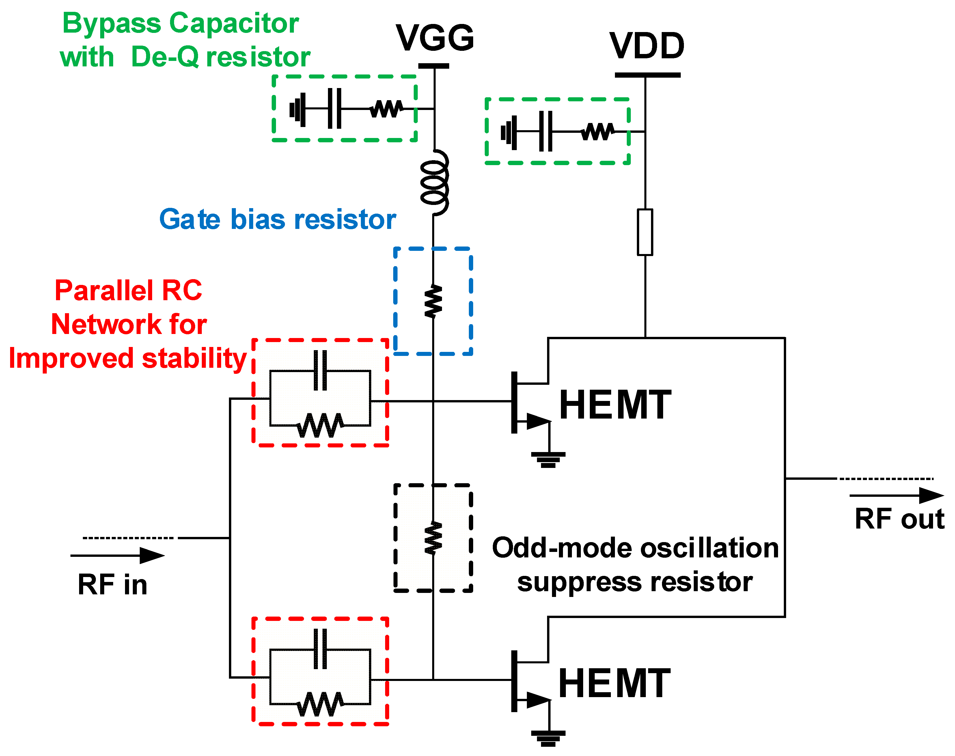
The schematic of the 32 GHz HPA is presented in
Figure 1. A cascaded two-stage common source (CS) amplifier topology is used to achieve more than 15 dB gain at the operating frequency. To achieve an output power higher than 38 dBm, an eight-way power combining network in the current mode was employed to effectively combine the power delivered from the parallel output stages. For each parallel HEMT, a 50 Ω resistor is connected between each gate of the transistors to avoid any undesirable odd mode oscillation issues caused by the devices’ asymmetry from fabrication. As the HEMT devices operate at 25 V with a high-DC current, double metal layers were used for the bias line to minimize undesirable drops in voltage.
2.1. Device Selection and Stabilization
In this work, 150 nm GaN HEMT technology was used, which has an over 120 V gate-drain breakdown voltage and a 34.5 GHz cut-off frequency. There are two types of HEMT models depending on the backside via layout configuration. One is the outside the back via (OSV) HEMT and the other is the internal backside via (ISV) HEMT. With the same number of gate fingers and width, the OSV HEMT layout occupies a smaller area than that of the ISV HEMT. To minimize the chip area consumption, the OSV HEMT was used despite the fact that the ISV HEMT has better self-heating performance with a large number of vias on the backside. The class-AB configuration was selected to improve the power efficiency, and the device was biased to the drain supply of 25 V and the gate voltage of −1.55 V. Since the power driven by each stage is proportional to the total gate width of each stage, it is necessary to choose the optimal periphery ratio for the power efficiency for a given gain requirement. The gate periphery ratio of 3:8 was selected to obtain proper driving power from the driver stage (first stage) with a desirable power gain, and it guarantees the power stage (final stage) to achieve the desired output power. The size of the OSV HEMT used at the first stage (H1–4) was selected to be 6 × 50 μm, and the 8 × 50 μm OSV HEMT was used for the final stage (H5–12).
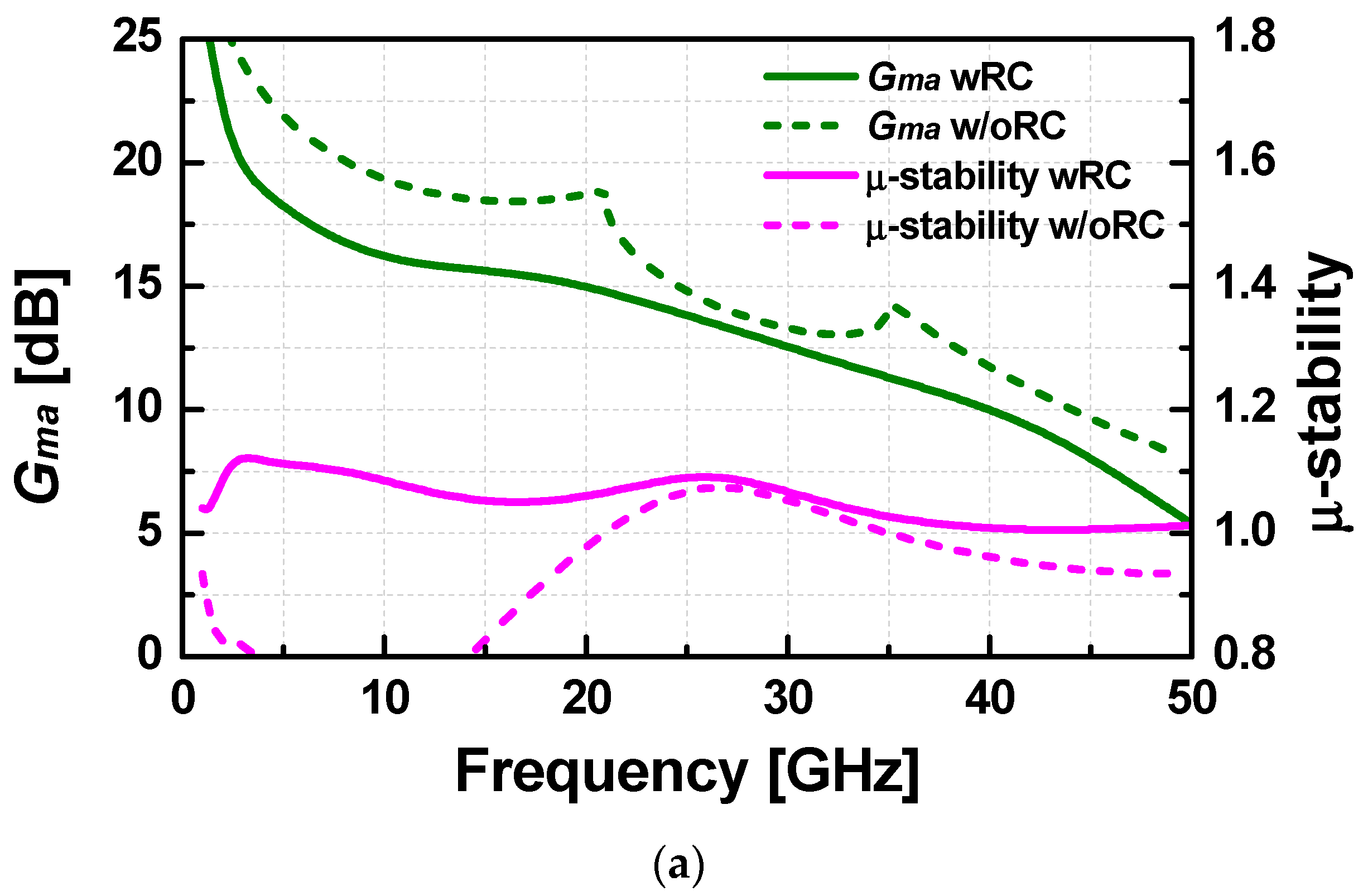
In designing a robust high-power amplifier (HPA), stable operation of the HPA is essential. In this work, a parallel RC network at the gate was employed to improve stability, especially at a low-frequency region. Since the parallel RC network at the gate of each HEMT degrades the power gain and efficiency, it is critical to determine the proper values of the resistance and capacitance of the parallel RC networks for a high-performance HPA design. To guarantee unconditional stability from 100 MHz to 50 GHz, the parallel RC network comprised a 40 Ω resistor and a 580 fF capacitor for the 6 × 50 μm OSV HEMT and a 50 Ω resistor and a 630 fF capacitor for the 8 × 50 μm OSV HEMT.
Figure 2 shows the simulated maximum power gain (
Gma) and the
μ-stability factor of the 6 × 50 μm and 8 × 50 μm OSV HEMT devices. The
Gma at 32 GHz is reduced from 13.1 dB to 12 dB for the 6 × 50 μm OSV HEMT device and from 14.4 dB to 11.5 dB for the 8 × 50 μm OSV HEMT device. Meanwhile, the device itself is unconditionally stable with
μ > 1 from 100 MHz to 50 GHz.
Figure 2 presents the effects of the parallel RC network on the maximum available gain (
Gma) and
μ-stability with and without the parallel RC network. The simulated maximum frequency of oscillation (
fmax) of the 6 × 50 μm and 8 × 50 μm OSV HEMT devices is 62.6 GHz and 54.4 GHz, respectively.
In combining multiple parallel HEMT devices, there is a possibility of odd-mode oscillations, which can be caused by the electrical asymmetry from the differences in the transconductance, biasing current, and nonlinear parasitic capacitors. It is noted that the odd-mode instability is not predictable from either the
μ or K-Δ stability factor from the small signal S-parameter simulations. To suppress unpredictable instability, resistors are placed between the paralleled transistor branches [
14].
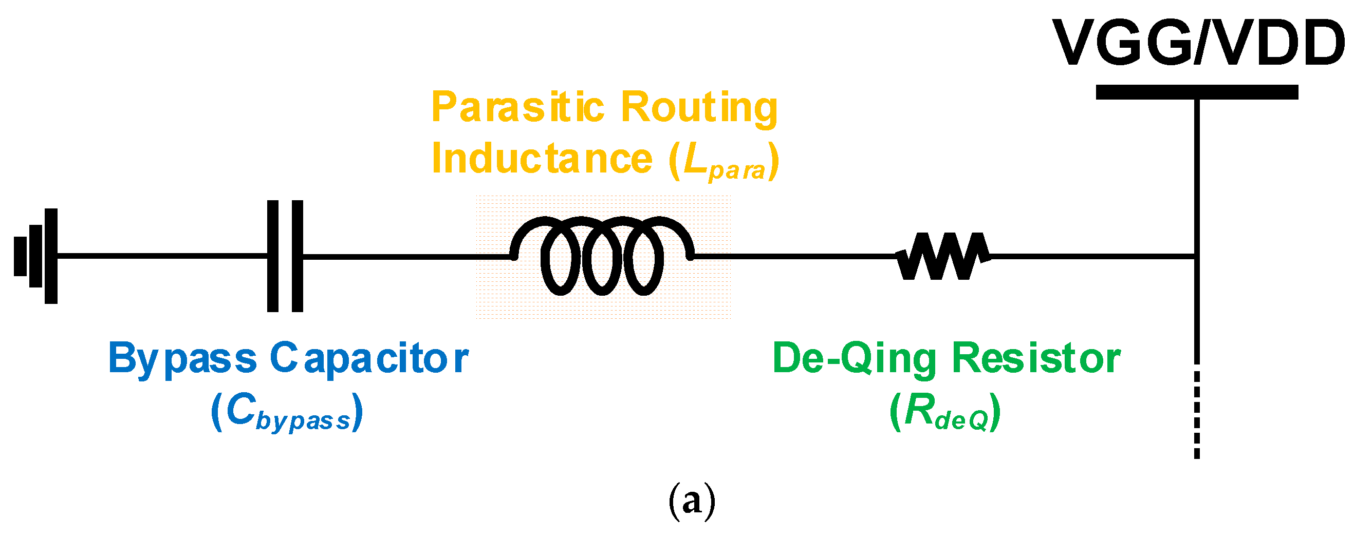
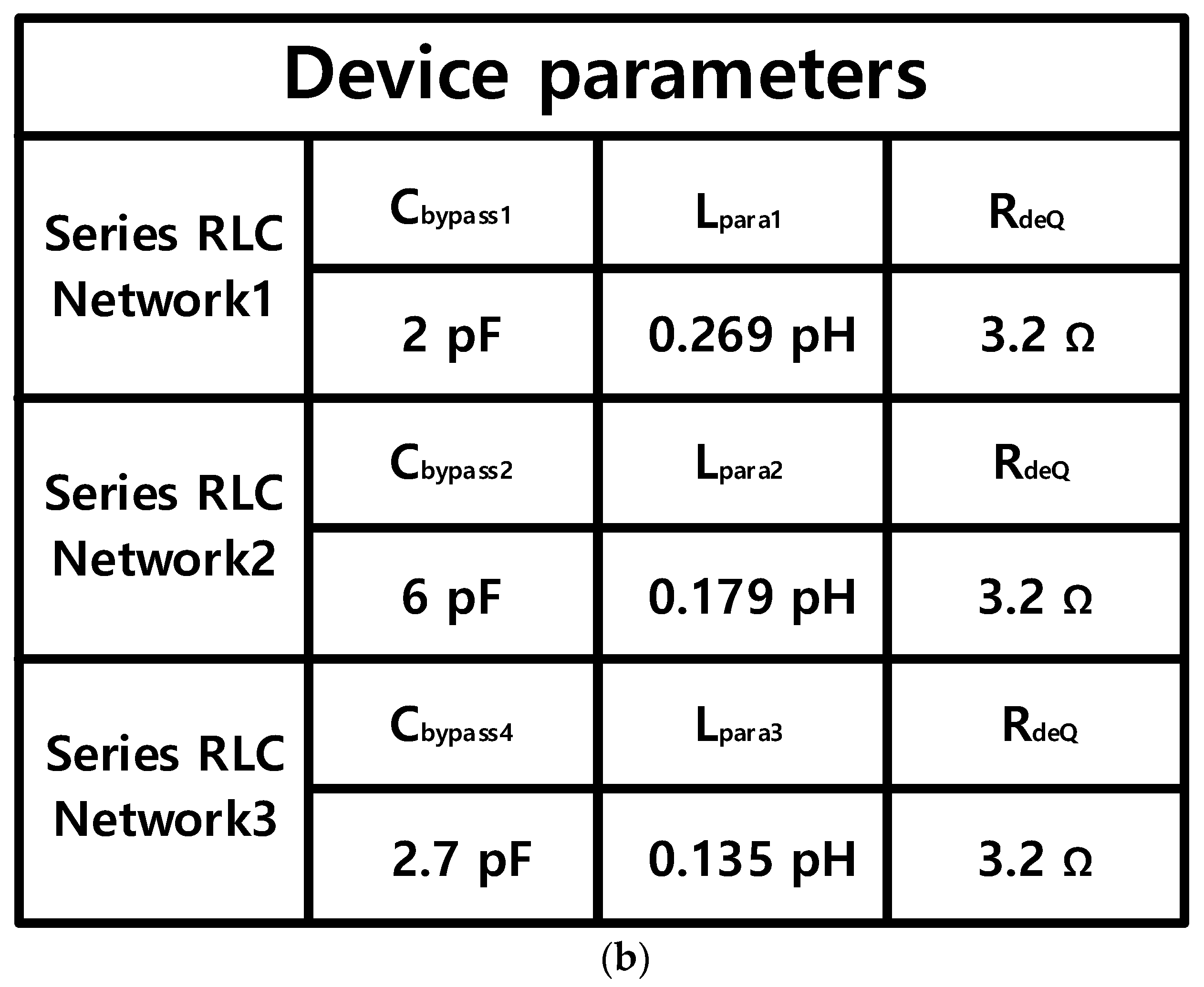
Sufficient bypass capacitors are essential to suppress noise, interferences, and RF leakages through the bias circuits. To improve the stability of the HPA, we added a de-Qing resistor in series with the bypass capacitor to suppress the ringing of the series RLC network from the parasitic routing inductance (
Lpara). It is important to select a proper series resistance since the de-Qing resistor trades off with the performance of the filtering capacitance. To keep the series RLC network in the over-damped oscillation, the series de-Qing resistor
RdeQ should meet the condition provided by:
where
Lpara is the routing inductance and
Cbypass is the bypass capacitance.
It is noted that
Lpara should be minimized to keep
RdeQ small enough not to degrade the filtering performance. The values of
Lpara1-3 were estimated from the ADS momentum simulation and the value of
Cbypass was determined to meet the over-damped oscillation condition as a function of the de-Qing resistor in time domain simulations. The parameters of the series RLC network of the bypass capacitor with de-Qing resistors are presented in
Figure 3.
A simplified block diagram of the implemented stabilization circuits is illustrated in
Figure 4.
2.2. Impedance Matching Network Design
In designing the HPA, an ADS momentum simulator was used to optimize the transmission lines for accurate impedance matching higher frequencies. The design procedure involves careful EM simulation with backside vias formed through a thick SiC substrate to avoid frequency shift and impedance mismatch. In this work, an additional backside via inductance of 32 pH was included in series with the via model from the process design kit (PDK). Since GaN HEMT has relatively large transconductance, it is crucial to guarantee the amplifier stability at the low-frequency region. Thus, the matching network was carefully designed to suppress undesired low-frequency signals below the target frequency. The out-of-band gain should be less than 0 dB to eliminate the possibility of instability at low frequencies. Due to the difficulty of accurately implementing the required inductance with lumped inductors from the PDK and layout restrictions, all the matching networks comprised the transmission lines with lumped capacitors by trading off the area occupancy and matching performance. Compared with a spiral lumped inductor, a transmission line is more promising at the Ka-band considering the SRF and the layout inconvenience of the spiral inductors. Moreover, a more accurate impedance-matching circuitry can be implemented with transmission lines throughout the momentum simulation in the ADS. Different from the series inductance, a lumped capacitor was used for the shunt capacitance in the matching networks since it has a relatively higher SRF than a lumped inductor, with more compact area occupancy compared with its distributed counterpart. The output matching network determines the power delivered to the load and the power-added efficiency (PAE). Load-pull simulations were used to determine the optimum output-matching impedance. A load-pull simulation of the 8 × 50 μm OSV HEMT is presented in
Figure 5. The load-pull simulation was performed with the parallel RC network at the gate with a power contour step size of 0.8 dB and a PAE contour step size of 5%. The maximum power delivery was 27.2 dBm at optimum impedance
Zpout_opt = 9.2 + j35.8 Ω, and the maximum PAE was 38% at optimum impedance
ZPAE_opt = 4.8 + j37.5 Ω. The input impedance of the output matching network from 28 GHz to 32 GHz is also shown in
Figure 5. To achieve a high-outpower level, the output matching network has an input impedance of
Zin = 12.7 + j36 Ω, which is close to
Zpout_opt at 32 GHz. The output matching network combines the output power amplified by each HEMT device. There are losses due to the structures combining the output power, which will inevitably occur, and consideration is required. The loss of the designed combiner (output matching network) at 32 GHz is 1.47 dB, which is an acceptable value for the eight-way combiner.
3. Simulation and Measurement Results
The proposed 32 GHz power amplifier was designed in 150 nm GaN HEMT technology with an
fT of 34.5 GHz.
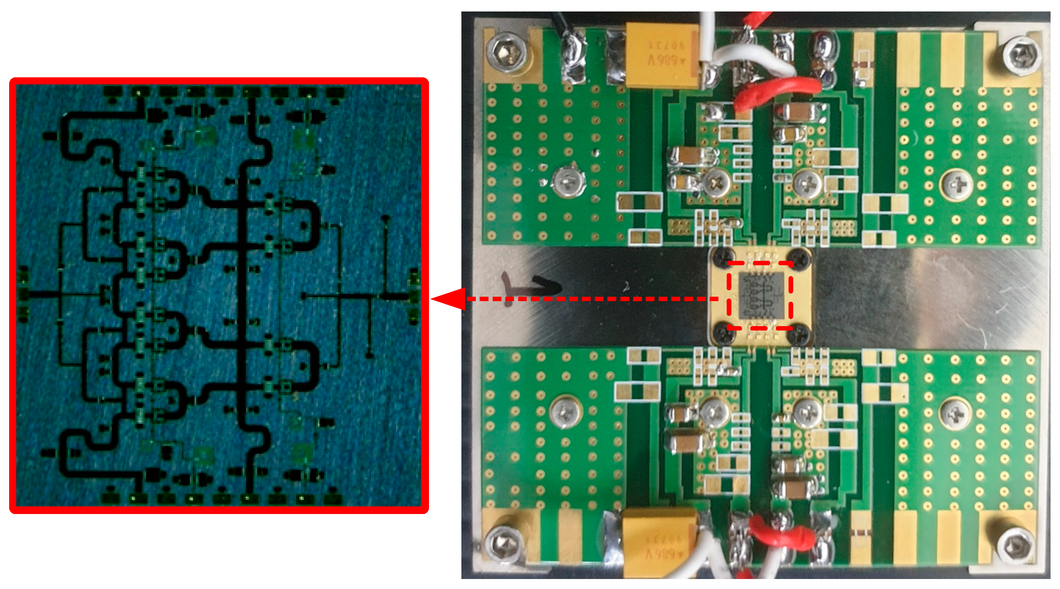
Figure 6 shows a photograph of the implemented amplifier and the chip on board (CoB) for the measurement purpose. The implemented MMIC occupies an area of 4.3 mm × 4.5 mm (19.35 mm
2), including all the RF, ground, and DC pads. In order to construct a reliable CoB, there are various technicalities to consider. While epoxy is the most widely used die-attach material during packaging, special attention should be paid to the removal of voids or fumes generated during the hardening process of the epoxy, which can cause instability of the MMIC amplifiers. We used eutectic bonding as the die-attachment material to avoid undesired instability due to the parasitic capacitance from the voids formed in the epoxy. Eutectic bonding utilizes the properties of alloys that can melt at low temperatures to help handle sensitive products at high temperatures, such as integrated circuits. In this work, a preform with a composition of 80% gold and 20% tin (80Au20Sn) was used. The high solubility between the materials of the eutectic agent enables strong binding and stable connections. It also possesses excellent electrical and thermal conductivity, making it suitable for applications that involve a large amount of heat generation and dissipation.
The external bias circuitry in the board comprises single-layer capacitors, ferrite beads, chip capacitors, and resistors. A large inductance generated by a relatively long bonding wire also heats the stability of the HPA under test due to the increased reactance in the path of the bias lines. To mitigate this effect, single-layer ceramic capacitors were placed in the vicinity of the DC pads of the packaged MMIC. In the implemented board, single-layer capacitors of 100 pF and 300 pF were employed for external gate and drain bias lines. To ensure the stability of the bias line and reduce noise from the power supply, ferrite beads were used to provide high series resistance at high frequencies, which dissipates the noise power in the form of heat. In implementing a reliable external biasing circuitry, multiple chip capacitors with a different self-resonance frequency (SRF) are used with de-Qing resistors in series (a combination of a 0.1 μF shunt capacitor, a 1 μF capacitor with a 3 Ω de-Qing resistor, a 50 μF capacitor with a 20 Ω de-Qing resistor). While improving the stability of the MMIC HPA by adding series resistors in the gate bias line, it is important to note that an excessively high series resistor in the gate bias line may lead to a more positive gate bias voltage due to the gate leakage current. Thus, a proper resistor value should be selected. Here, we placed a 50 Ω resistor in series for the gate bias line.
We measured the power amplifier’s small signal (S-parameters: S11, S12, S21, and S22) and large signal performance. DC bias was supplied by a Rohde & Schwarz (R&S) HMP4040 device. The S-parameters were measured with the vector network analyzer R&S ZNB40. During large-signal measurements, the waveform generator Keysight 33250A generates a pulse-modulated signal with a 10% duty cycle and 1 ms pulse. The input signal was generated from a signal generator, R&S SMA100B, and for measurement at a high-input-power level, a driving amplifier was used. To prevent returned signals from the reflection, an isolator, Fairview Microwave FMIR1036, was used between the driving amplifier and the designed power amplifier. The output power was measured with a spectrum analyzer, R&S FSV3044. A block diagram of the measurement setup for the small signal is illustrated in
Figure 7.
Figure 8 shows a block diagram of the setup for large-signal measurement.
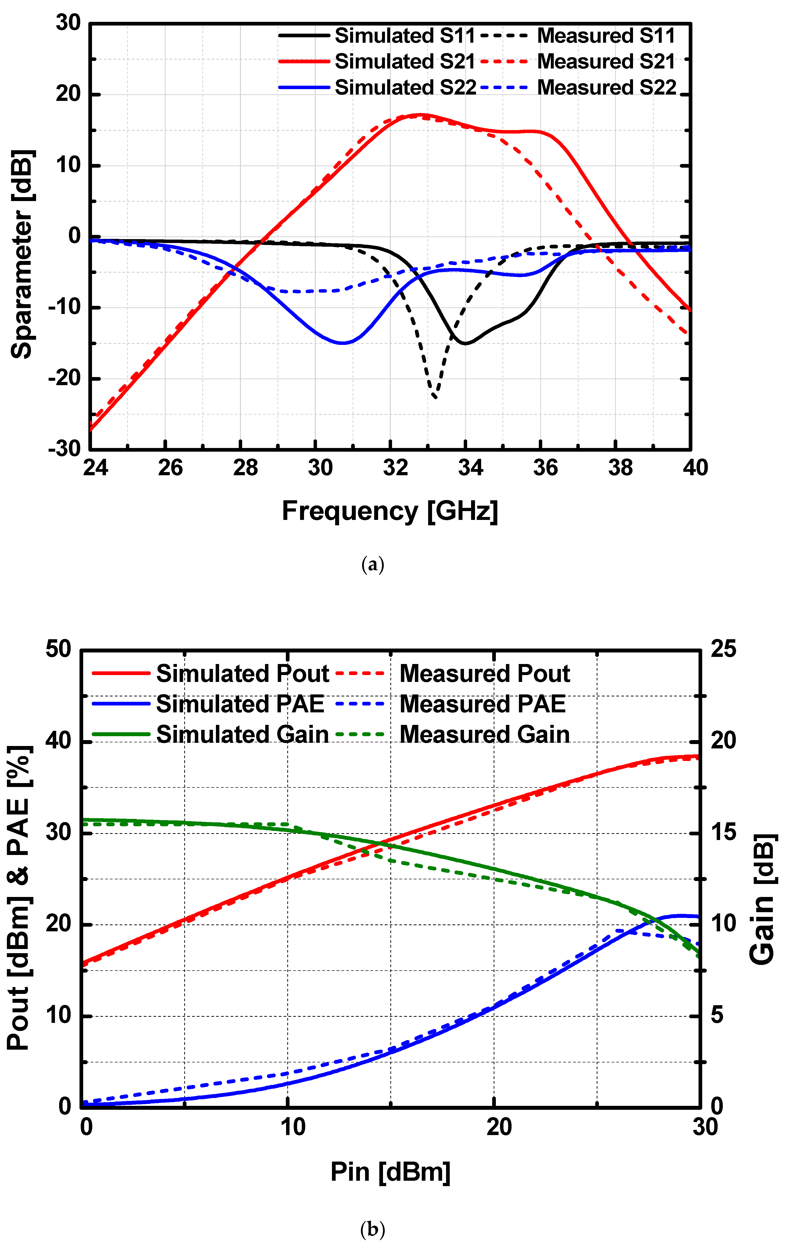
The measured small-signal and large-signal performance are presented in
Figure 9. The gain at 32 GHz is 16.4 dB, and the 3 dB gain bandwidth was 3.5 GHz between 31.3 and 34.8 GHz. The gate bias voltage was
VGG = −1.55 V and the drain supply voltage was
VDD = 25 V with a total drain current of 410 mA.
As shown in
Figure 9a, the maximum gain was 16.9 dB at 32.7 GHz, and the 3 dB gain bandwidth was 3.5 GHz between 31.3 and 34.8 GHz with a sharp roll-off skirt. During the large signal test at 32 GHz under a 10% duty cycle and 1 ms pulse, the P
sat was measured to be 38.3 dBm (6.76 W), and the power gain was 7.3 dB. The peak PAE was 19.3%, and the output of 1 dB gain compression point (OP1 dB) was around 28.5 dBm. The measurement results corresponded well with the simulations with small degradations at the high-frequency regime.
Table 2 summarizes the performance of this work in comparison with the recently reported Ka-band power amplifiers. The proposed design has the best small-signal gain and 3 dB gain bandwidth performance compared with the other two-stage designs in the Ka-band.


 ,
, 


