Article

Design and Implementation of a Planar MIMO Antenna for Spectrum-Sensing Applications

1
Department of Electronics and Communication Engineering, SRM Institute of Science and Technology, Kattankulathur 603203, India
2
Department of Electronics and Communication Engineering, Netaji Subhas University of Technology (East Campus), Delhi 110031, India
3
Department of Electronics and Communication Engineering, Dr. B. R. Ambedkar National Institute of Technology, Jalandhar 144011, India
4
Department of Information Technology, College of Computer and Information Sciences, Princess Nourah bint Abdulrahman University, P.O. Box 84428, Riyadh 11671, Saudi Arabia
5
School of Electronic and Electrical Engineering, Kyungpook National University, Daegu 41566, Republic of Korea
*
Author to whom correspondence should be addressed.
Electronics 2023, 12(15), 3311; https://doi.org/10.3390/electronics12153311
Submission received: 22 June 2023 / Revised: 15 July 2023 / Accepted: 31 July 2023 / Published: 2 August 2023
(This article belongs to the Section Microwave and Wireless Communications)

Abstract

:
Spectrum sensing is an important aspect in cognitive radio (CR) networks as it involves the identification of unused frequency spectra, which saves both bandwidth and energy. The design of a compact super-wideband (SWB) multi-input multi-output (MIMO)/diversity antenna with triple-band-notched features is presented for spectrum sensing in CR systems. The MIMO antenna comprises four identical semi-elliptical-shaped monopole resonators, which are orthogonally positioned and excited individually via tapered coplanar waveguide feed lines. Also, a mirror-slot analogous to the radiator is etched in the ground conductor of each antenna element to achieve SWB characteristics. In order to avoid interference with the SWB, the antenna radiator is loaded with a staircase-shaped slit and a pair of concentric slits, arranged like a complementary split-ring resonator. The antenna resonates from 1.2 to 43 GHz, exhibiting a bandwidth ratio of 36:1. In the MIMO antenna, the antenna elements are located orthogonally, and the isolation > 18 dB and envelope correlation coefficient < 0.01 are realized in the resonating band. The antenna offers a peak gain of 4 dBi, and a sharp reduction in gain at notch frequencies (3.5 GHz, 5.5 GHz, and 8.5 GHz) is achieved. The size of the MIMO antenna is 52 mm × 52 mm. The proposed compact-size antenna features a high bandwidth ratio and straightforward design procedure, and can be simply integrated into contemporary RF equipment. The presented SWB MIMO antenna outperforms SWB antenna designs reported in the open literature, which featured one or two notched bands, whereas it has three notched bands. Also, the three notches in the SWB are achieved without the use of any filters, which simplifies the antenna development process.

1. Introduction

Cognitive radio (CR) technology detects unused frequency spectrum and uses it efficiently by adapting to the needs of the radio network. The spectrum-sensing ability of the used hardware determines the communication reliability and continuity in CR networks. Super-wideband (SWB) antennae with a bandwidth ratio of 10:1 (or greater) are preferred for spectrum sensing in CR applications [1,2,3,4,5]. An antenna is an essential element in the transmission and reception of electromagnetic signals. Printed monopole antennae are preferred for SWB transceiver systems due to their low-profile, compact size, their lightweight nature, and their ease of integration with other circuits [6,7,8]. The only issue with SWB antennae is their limited operating range, which is caused by low transmission power. Several SWB monopole antennae with different geometries have recently been reported by numerous researchers [9,10,11,12,13,14,15]. In [9], an antenna with SWB range was presented that consisted of a conventional circular-shaped patch, a tapered feed line, and a rectangular-shaped ground surface, with a frequency ratio of 16:1. Multiple notched bands are obtained in the SWB of the reported antenna. In [10], a Mickey-Mouse-shaped antenna with a semi-elliptical ground was reported for SWB applications, with a frequency ratio of 32:1. A modified circular-shaped patch was designed for SWB coverage in [11], with flared-out feed lines exciting the resonator. Two notch bands were also achieved by using circular rings loaded in the modified circular-shaped radiator. In [12], a coplanar waveguide (CPW)-fed semi-circular-shaped antenna was designed with transparent plexi-glass and a solar panel to power mobile devices. In [13], an offset-fed elliptical ring-shaped antenna for SWB applications was designed, with the antenna radiator fed through a tapered feed line to achieve impedance matching. In [14], an SWB Vivaldi antenna design for lower 5G bands was presented, with wideband performance achieved by using ten corrugated and two circular slots in the metallic flares of the resonator. An SWB on-chip antenna with a small footprint and high gain was demonstrated in [15], and it was developed using a micromachining technique. However, all of the previously reported antenna structures have a single element and use conventional geometries that occupy a large chip space, and it could be challenging to design and integrate them in contemporary RF devices.
Self-complementary antennae (SCAs) are also preferred in SWB systems. Typically, an SCA consists of a radiating element and a slot, which complements the radiator geometry, etched in the ground plane. The idea of the self-complementarity and constant input impedance property of the antenna was proposed by Y. Mushiake [16]. Various planar, solid, axially symmetric, log-periodic antenna structures based on the concept of self-complementarity were reported for the SWB [16,17]. In [18], a monopole antenna with a radiator-shaped complementary slot embedded on the ground surface was presented. In [19], a monopole quasi-self-complementary antenna (QSCA) consisting of a half-circular radiator was suggested. A CPW-fed inverted L-type QSCA was presented in [20]. A semi-elliptical complementary monopole antenna possessing a band elimination capability was presented in [21].
Diversity approaches can be used effectively to solve the multipath fading problem in wireless systems. Diversity systems improve the efficiency of a radio channel without increasing transmission power. The most common diversity methods are frequency, time, polarization, and space. Among these, space diversity, also known as antenna diversity, is widely used because the receiver configuration is quite simple in it. Space diversity employs multiple antenna elements at the transmitting and receiving terminals to obtain multiple uncorrelated copies of the transmitted signal. Also, when compared to single-element antennae, multi-input multi-output (MIMO)/diversity antennae exhibit a higher data rate, better link reliability, and robustness [22,23,24]. The compactness of the antenna is also a key concern while designing portable/handheld equipment. The space between identical radiating elements must be minimised to design compact MIMO antenna configurations. However, this reduces isolation between the adjacent antenna elements and deteriorates the overall performance of the MIMO antenna.
A compact SWB semi-elliptical-self-complementary (SESC) four-element MIMO/diversity antenna is proposed in this paper. A tapered line CPW feed is used for matching the 50 Ω input impedance of the coaxial connector. Since the MIMO antennae with separated ground plane conductors are not preferred in practice, due to varying level of reference voltage among the ground planes [25], the radiators’ ground patches are linked together in the proposed MIMO antenna design. The MIMO antenna resonates (S11 ≤ −10 dB) in the range of 1.2 to 43 GHz, exhibiting the bandwidth ratio of 36:1, with triple-notched bands at 5.5 GHz (WLAN), 3.5 GHz (Wi-MAX), and 8.5 GHz to eliminate interference in the C-, S-, and X-bands, respectively. The polarization diversity and high inter-element isolation are achieved by the orthogonal arrangement of the antenna’s radiating elements. Due to the use of an elliptical-shaped radiator, the presented antenna design is fairly simple, and it offers triple-band rejection capabilities, which enhances the performance of the communication system. Also, the proposed SWB antenna is relatively small, making it appropriate for use in miniaturized RF devices and monolithic microwave integrated circuits. Hence, the suggested antenna outperforms the reported SWB antennae due to its simple design, small size, and multiple notched bands.

2. Related Works

In contrast with a two-port MIMO configuration, where each element is coupled with only one nearby radiator, designing a small four-port MIMO configuration is more challenging, as each antenna element is affected by three neighbouring radiators [26]. An ultra-wideband (UWB) MIMO design with two identical circular-shaped QSCAs located in mirror fashion was presented [27]. A quad-element UWB QSCA design comprising two different radiating patches and a slotted ground surface was reported [28]. A dual-port UWB MIMO QSCA with two notches was presented [29]. An SWB antenna structure consisting of two quarter-circle monopole patches and a ground surface arranged orthogonally to achieve polarization diversity was proposed [30]. The bandwidth ratio of the antenna was 26:1, but it was large-sized (130 mm × 120 mm). A dual-port UWB antenna, comprising of inverted-A monopole elements with triple-band rejection characteristics (C-band, LTE band-43, and IEEE 802.11ac), was proposed [31]. In [32], a planar quad-port notched-band antenna comprising circular monopole elements, a defected ground surface (DGS), and an electromagnetic band gap (EBG) structure was investigated. A dual band-notched MIMO antenna comprising four rectangular-shaped radiating elements was suggested for UWB applications [33]. A CPW-fed UWB MIMO antenna with two notched bands (at 4.8 and 7.7 GHz) was developed for wireless communication applications [34]. A two-port SWB MIMO antenna with modified feather-shaped radiators was proposed [35], where a metal strip was added between the resonators to improve correlation among antenna elements. A compact SWB MIMO antenna comprising hexagonal Koch fractal-shaped radiators was presented [36]. In this antenna design, a meander line decoupler was built from the ground plane to improve mutual coupling. A two-element SWB MIMO antenna was presented in [37], where a step impedance microstrip line was used to excite the radiator. An SWB MIMO antenna with spade-shaped resonating elements was proposed [38], where DGS and a windmill-shaped decoupler were used to increase isolation. An SWB MIMO antenna consisting of four monopole radiators with separated ground planes was reported in [39]. In [40], a quad-port SWB MIMO antenna configuration was presented with four wheel-shaped radiators separated by a windmill-shaped decoupling structure to achieve isolation. In [41], a four-element SWB MIMO antenna was presented with an array of metamaterial unit cells used as a superstrate to improve gain and isolation. The reported SWB antenna designs are mostly fed using a microstrip feed line and are relatively large-sized with complex geometry. And the reported self-complementary MIMO antenna designs were mostly used for dual-port systems only.
Table 1 shows a comparison of the proposed MIMO antenna design to other reported wideband antennae. In contrast to the above-reported antenna designs [27,28,29,30,31,32,33,34,35,36,37,38,39,40,41], the designed SWB MIMO antenna is novel in terms of size, the number of resonating elements, bandwidth ratio, and notch bands. The proposed CPW-fed antenna elements with common ground planes can be easily incorporated into the matching networks or portable monolithic microwave integrated circuits (MMICs). A common ground plane ensures an equal reference voltage among the elliptical-shaped resonators. The rejection of interfering bands from the SWB is achieved by etching a staircase-shaped slit and complementary split-ring resonator (CSRR) from the radiating element of the antenna. This simplifies the antenna configuration as additional active devices or separate filter circuitry are not required to remove the interfering signals.
The following are the main highlights of the presented work:
  • The bandwidth ratio of the suggested antenna is significantly high when compared to the reported antenna structures.
  • The SWB antenna designs proposed in the open literature featured one or two notched bands, whereas the suggested SWB antenna has three notched bands.
  • The three notches in the SWB are achieved without using any filters, which streamlines the antenna development procedure.
  • The suggested SWB antenna occupies relatively little space and may be readily incorporated into compact-size RF equipment.

3. Antenna Configuration

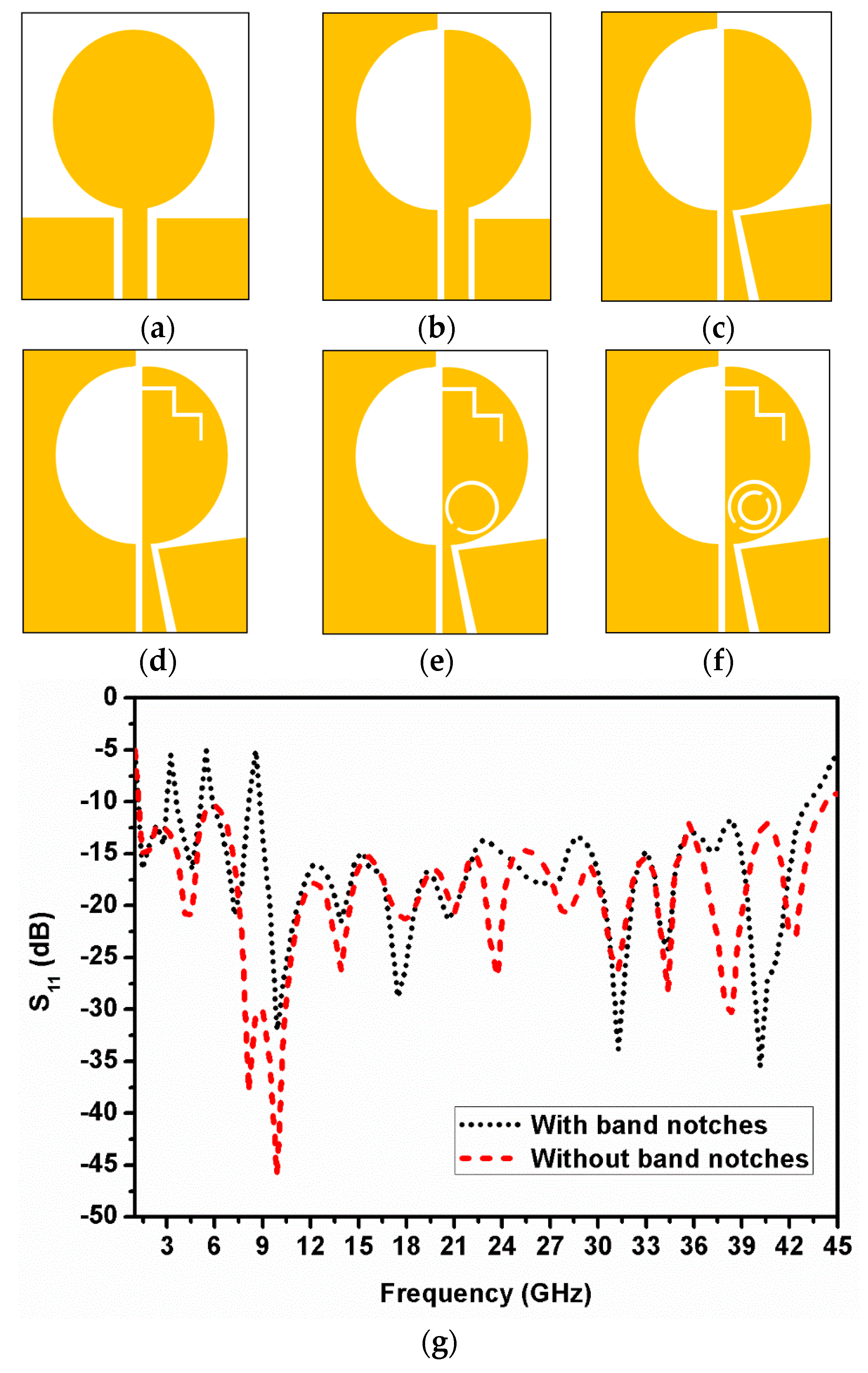
3.1. Design of SWB SESC Antenna Element with Triple-Band Notches

The geometry of the SESC antenna is shown in Figure 1. The antenna comprises a semi-elliptical monopole radiating element excited by a CPW feed line, as shown in Figure 1a. A mirror-slot, analogous to the shape of the metallic resonator, is cut out from the ground conductor of the antenna to construct the SESC antenna element possessing SWB characteristics. A1 and B1 are the respective semi-major and semi-minor axes of the complementary slot. And B2 and A2 are the semi-minor and semi-major axes of the elliptical resonator, respectively. The SESC antenna illustrates higher eccentricity for sustaining modes of a higher order to obtain broad bandwidth. The antenna is designed on a 1.6 mm-thick FR-4 dielectric substrate (tan δ = 0.02, ɛr = 4.4) of size 26 mm × 31 mm. Since the input impedance of the SESC antenna does not match the front-end impedance of standard RF equipment, a tapered CPW feed line is provided to match the antenna with the standard 50 Ω source impedance. The proposed SWB SESC antenna schematic with slits (Sa, Sb, and Sc) is given in Figure 1b, and the dimensions of the slits are given in Figure 1c. The 3-D electromagnetic (EM) simulator tool Ansys HFSS® is used for antenna designing. The dimensions of the antenna are given in Table 2. The localization of band notches is based on the intensity of the current distribution. The current pattern on the antenna element is observed in the Ansys HFSS simulator at the notched frequency bands, and the dimensions of the notched element are calculated and optimized to achieve a sharp notch at the interfering frequency bands.

Design Methodology

Figure 2 depicts the various phases involved in the development of the SESC antenna element. Considering the self-complementary principle, a semi-elliptical design is chosen to develop an antenna with a very large operational bandwidth. The input impedance (Zin) of an SCA is evaluated through the Mushiake’s relationship [16].
Zin = Z0/2 ≈ 60π
This relationship reveals that neither the antenna dimensions nor operational frequency (or bandwidth) of a well-designed SCA has a direct influence on its input impedance [3].
Figure 2a represents a conventional elliptical patch monopole antenna with a CPW feed and rectangular ground plane (Phase-1). The CPW feed offers a wide impedance bandwidth and simple device integration due to the presence of a metallic layer on only one side of the dielectric substrate. The ground plane of the antenna is extended in Figure 2b, and the radiator is modified to a semi-elliptical shape (Phase-2). A semi-elliptical shape slot, similar to the shape of the radiator, is also introduced in the extended ground plane to achieve SWB characteristics. In the next stage, the ground plane is tapered to achieve wide impedance matching, as shown in Figure 2c (Phase-3).
The reflection coefficients of the designed SESC antenna element are displayed in Figure 2g. The SESC antenna displays an impedance bandwidth of 1.2 to 43 GHz, which covers the C-, K-, Ka-, Ku-, L-, S-, and X-band wireless communication systems. Furthermore, to eliminate the common interfering bands from the SWB, the antenna radiator is loaded with a staircase-shaped slit (Sa), as shown in Figure 2d (Phase-4), and a pair of concentric slits (Sb and Sc), arranged like a CSRR, shown in Figure 2e,f (Phases-5 and -6), tuned at the centre frequencies of 3.5, 5.5, and 8.5 GHz, respectively.
The effective lengths of the slits (Sa, Sb, and Sc) for the respective notch-bands are obtained as follows [29]:
Sa = (L1 + L2 + L3 + L4 + Wa) ≈ 0.29λga
Sb = 2π(R1 + Wb) − G1 ≈ 0.52λgb
Sc = 2π(R2 + Wc) − G2 ≈ 0.52λgc
λg = c/frr,eff)0.5
εr,eff = (εr + 1)/2
where λg and fr correspond to guided wavelengths at notch-band frequencies, εr,eff is the effective dielectric constant of the substrate, and c is the velocity of light in free space. The band-notched effect of the three slits on the reflection coefficients is shown in Figure 2g.
The SWB SESC antenna vector current distributions at notch frequencies are visualized in Figure 3. The current vector flow in Figure 3a indicates that the effective length (Sa) of the staircase slit holds approximately a quarter-wavelength at 3.5 GHz. Further, as observable from Figure 3b,c, the split-ring resonators (Sb and Sc) are completely surrounded by the patch conductor. The current path is available along the (outer and inner) peripheries of these slits. As a result, two quarter-wavelengths are accommodated by the peripheral boundaries of the slits.
Thus, the effective lengths (Sb and Sc) of these slits are approximately equal to the half-wavelength at 5.5 and 8.5 GHz, respectively. At the corresponding frequencies, the flow of the current is in the opposite direction near the boundaries of the slits. Hence, the resulting fields get cancelled out and notched-band characteristics are obtained.

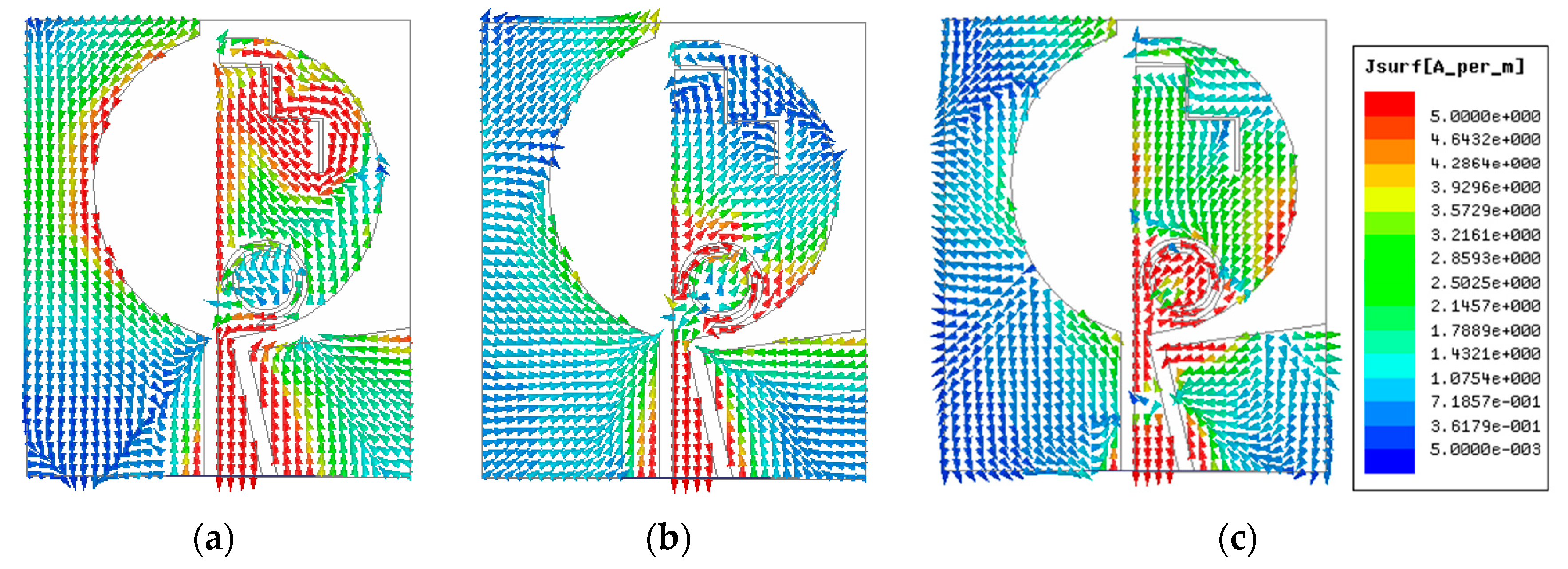
3.2. Design of SWB SESC Quad-Element MIMO Antenna with Three-Band Notches

The geometric layout of the proposed compact four-port MIMO antenna is presented in Figure 4a. The antenna is designed using four matching SWB SESC radiating patches placed orthogonally on the FR-4 substrate of size 52 mm × 52 mm × 1.6 mm. Each element of the MIMO antenna (for example, Radiator-1) is surrounded by two identical elements (Radiator-2 and Radiator-4) forming mutually orthogonal pairs (Radiator-1 and Radiator-2; and Radiator-1 and Radiator-4); therefore, the radiated fields are also mutually orthogonal to each other. The mutually orthogonal fields also reduce the mutual coupling, hence improving isolation among the resonating elements. The spacing between Radiator-1 and Radiator-3/Radiator-2 and Radiator-4 is sufficiently large (much larger than the adjacent pairs); therefore, a better envelope correlation coefficient (ECC) and isolation are obtained amongst the elements of the MIMO antenna.
Also, many researchers make use of an additional grounded stub (decoupling element) to achieve isolation between different elements of the MIMO antenna. In this work, the ground plane conductor (located centrally) is serving as a decoupling structure, thus reducing the inter-element coupling further. The ground patch conductor is designed to fit all four complementary slots in the MIMO antenna in a compact manner. The design details of the MIMO antenna are stated in Table 2.

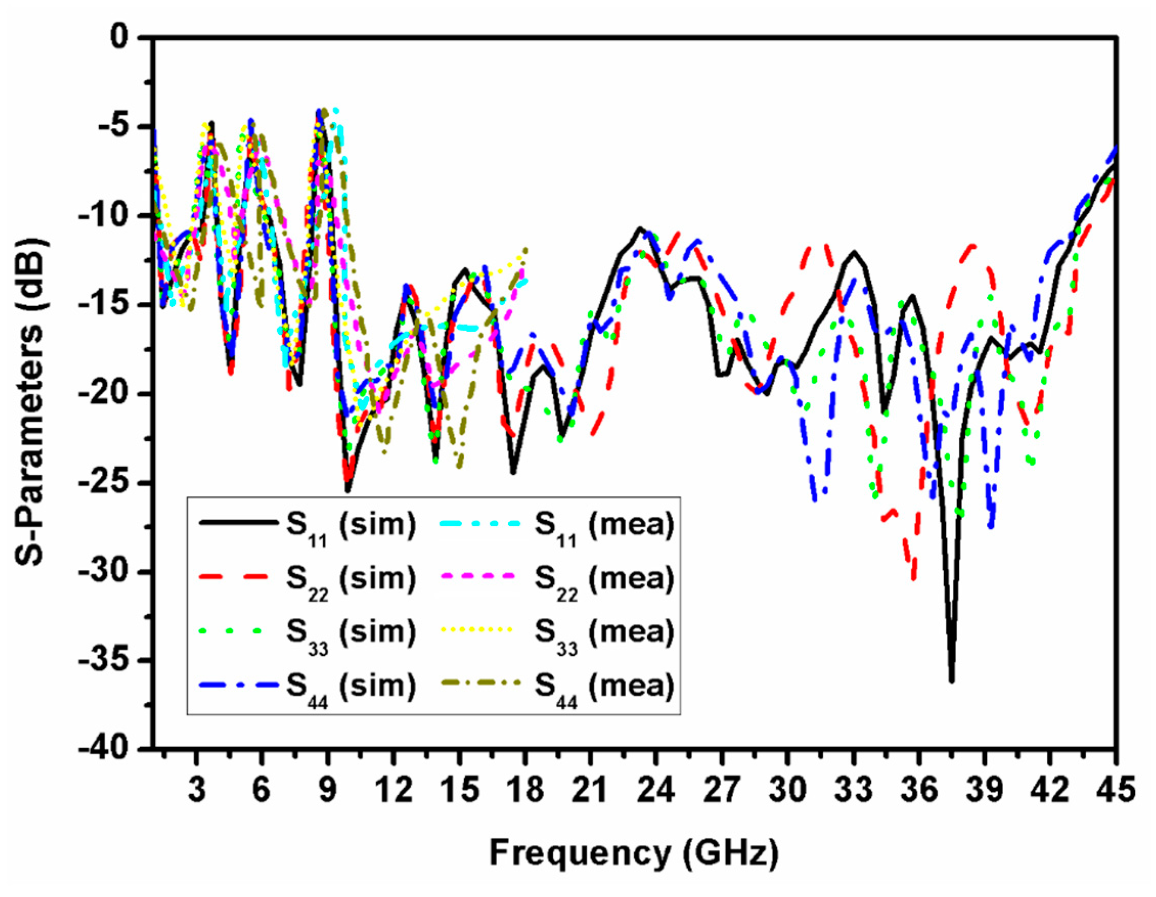
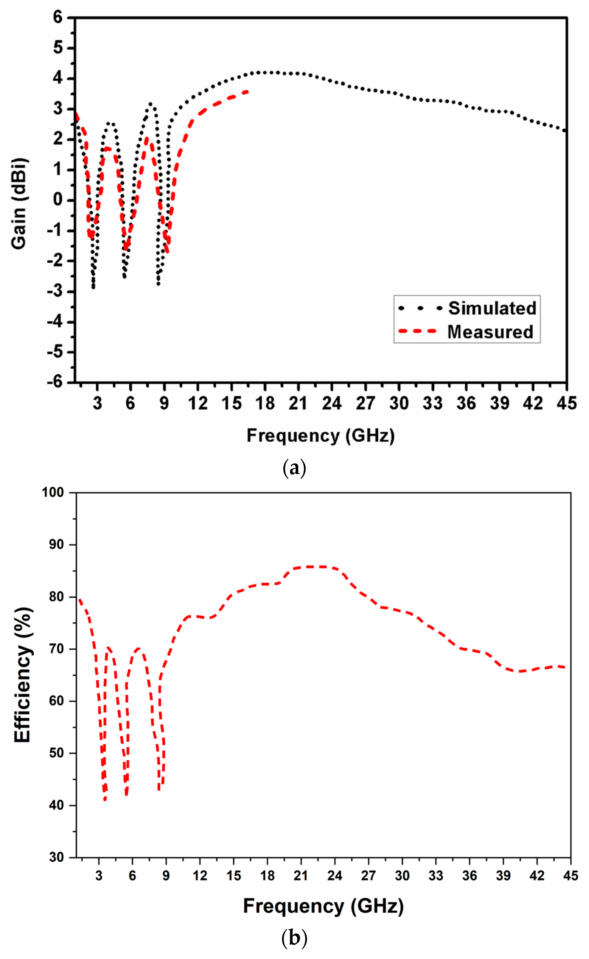
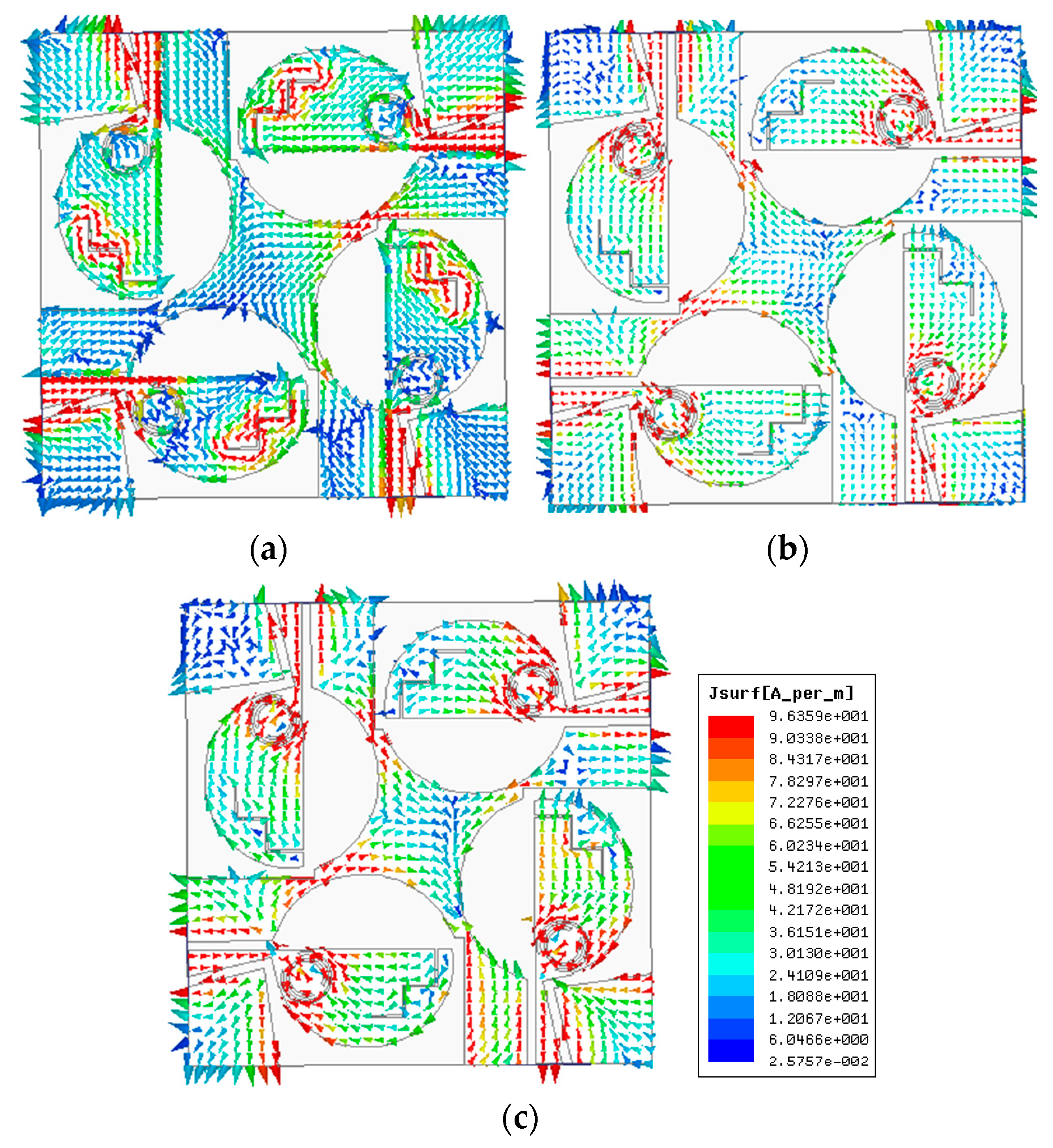
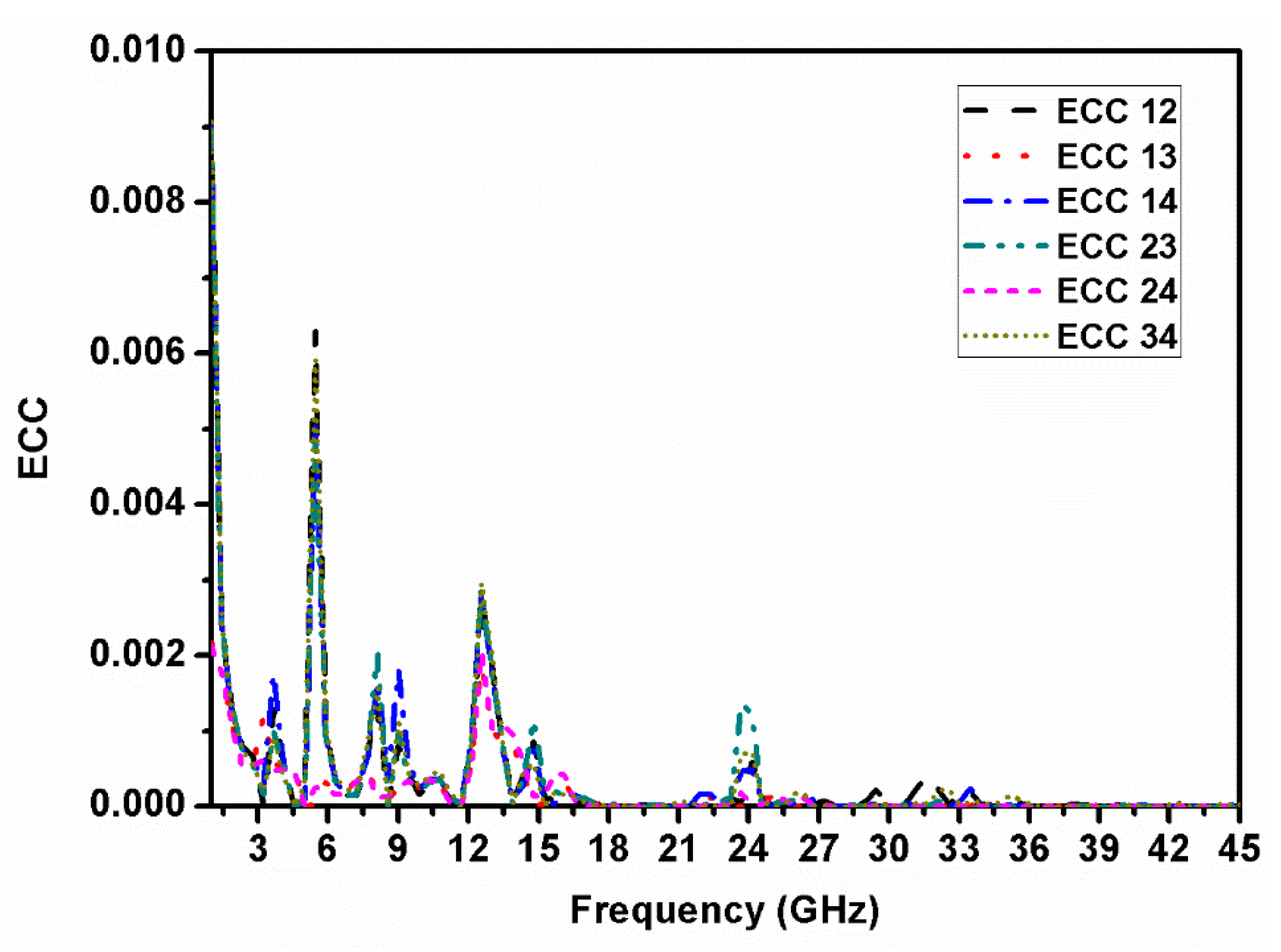
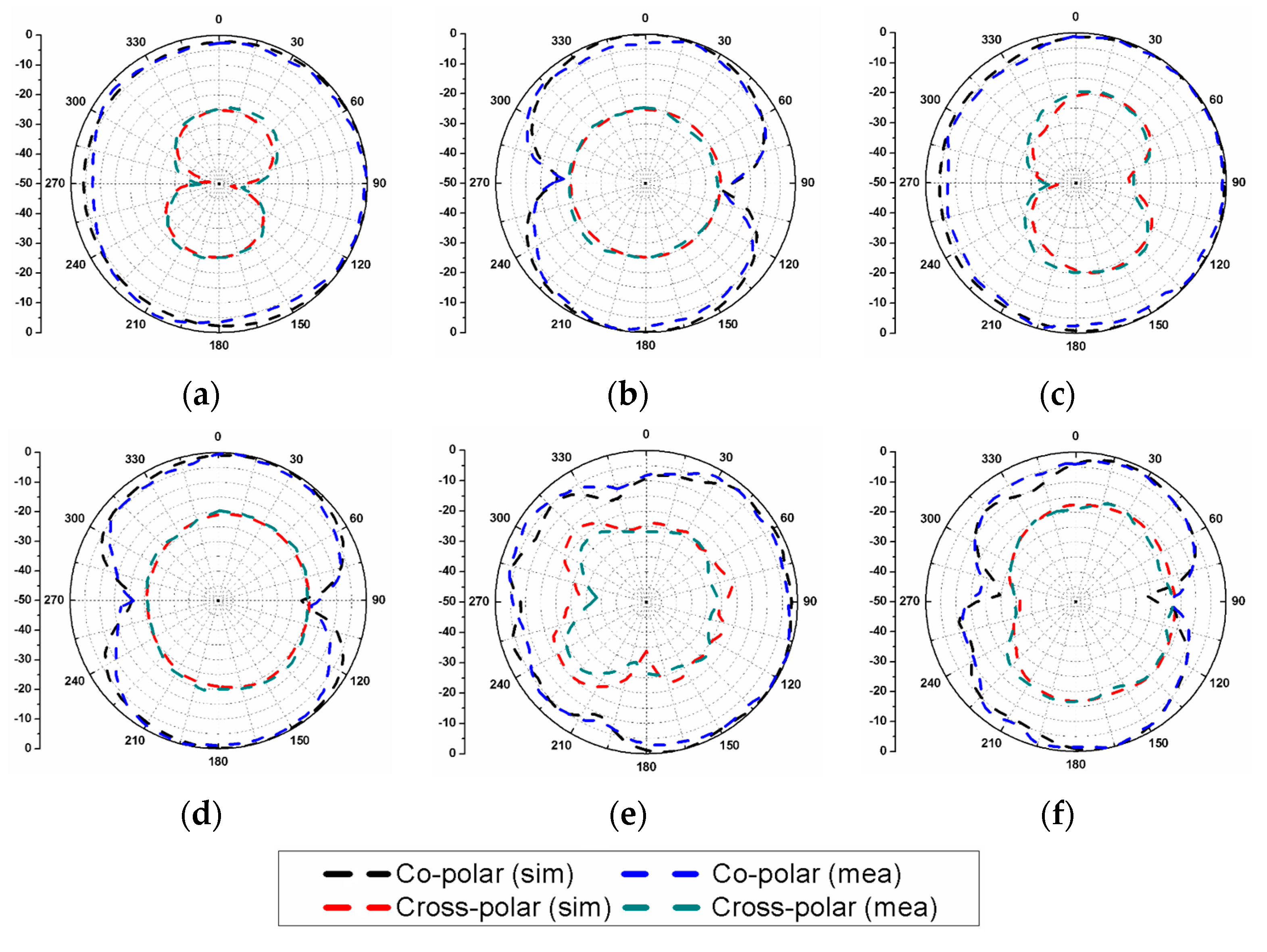
4. Results and Discussion

The MIMO antenna prototype is demonstrated in Figure 4b, and the antenna performance parameters are tested to verify the simulated results. The measurements are performed with the Anritsu S820D vector network analyzer. Figure 5 represents the reflection coefficients of the MIMO antenna. Excluding the notch bands, the antenna shows an impedance bandwidth from 1.25 to 43 GHz at all four ports. However, due to the obtainability of limited resources and SMA connector restrictions, the experimental results are taken up to 18 GHz only. During the measurements at Port-1, the other unused ports are matched by using the 50 Ω load. The bandwidth and other spectral characteristics are almost similar at all ports.
Figure 6a,b show the mutual coupling amongst various ports of the MIMO antenna. For a practical MIMO system, the minimum isolation between any two ports must be 15 dB [25]. The presented antenna exhibits isolation of more than 18 dB in the 12–15 GHz range, which further improves at higher frequencies. The distance between antenna radiators also affects the inter-element isolation. The diagonal components are separated by a much wider ground patch compared to the adjacent units. Due to this, the diagonal elements show better isolation (S31 and S42) compared to the adjacent radiating elements (S21, S41, S32, and S43).
Figure 7a illustrates the measured and simulated gain of the proposed antenna. A sharp reduction in the gain–frequency curve is observed at notch frequencies of 3.5, 5.5, and 8.5 GHz, whereas, at other frequencies, the designed antenna indicates suitable performance. The simulated efficiency of the presented SWB SESC antenna is shown in Figure 7b. At the notch frequencies, the efficiency curve sharply decreases, whereas, at other frequencies, the antenna exhibits reasonable efficiency.
Figure 8 visualizes the current vectors at corresponding band-notched frequencies with all four ports excited concurrently. The dominating current vectors (indicated as red) flow in opposite directions near to the periphery of the respective slits. This results in the cancellation of the resultant EM field at the respective notch-bands.
The diversity performance of the MIMO antenna can be expressed by ECC [42]. Figure 9 illustrates the ECC of the designed MIMO antenna, and it is noticed that the ECC is <0.01 in the entire resonating band. The simulated and measured outcomes of the co-polar and cross-polar radiation patterns are shown in Figure 10. The patterns are measured in an anechoic chamber, which consists of a standard receiving horn antenna and the proposed MIMO antenna, which are both rotated 360°. The Anritsu S820D VNA located outside the chamber is connected to the antenna positioner system via RF cables to capture the pattern values. It is noticed that near omnidirectional co-polarization patterns are attained in the H-plane, and cross-polarization is smaller than co-polarization in both the E-plane and the H-plane. However, at a few frequencies, the cross-polarization level upsurges, which is due to the horizontal component of the surface current on the radiating element.

5. Conclusions

In this paper, an SWB MIMO antenna with triple-band rejection features is designed. The antenna resonates from 1.2 to 43 GHz, exhibiting a bandwidth ratio of 36:1. The Wi-MAX, WLAN, and X-band interfering signals are suppressed by etching a CSRR and staircase-shaped slit from the radiator. The vector current distributions and realized gain of the antenna verifies the interference rejection at three frequencies. The designed SWB MIMO antenna has a small dimension and high bandwidth ratio with four radiating elements, which are usually needed for fast, secure, and reliable transmission. Low correlation and polarization diversity are achieved by locating radiating elements in an orthogonal manner. The MIMO antenna elements are excited by using a CPW feed, and their ground planes are also connected to each other, which facilitates the easy integration of the designed antenna with the matching network/portable MMICs. The designed MIMO antenna structure may be useful for multi-standard/multiband (C-, K-, Ka-, Ku-, L-, S-, and X-band) wireless communication systems and for spectrum sensing in CR applications. In the future, reconfigurability, as well as a larger number of radiators, can be introduced in the MIMO antenna, allowing it to operate efficiently in smart CR systems. The presented MIMO antenna could also be useful for IoT units and RF energy-harvesting systems.

Author Contributions

Conceptualization, S.K. and K.W.K.; methodology, D.K.R. and B.K.K.; software, D.K.R.; validation, S.K.P., H.C.C. and K.W.K.; formal analysis, S.K. and S.K.P.; investigation, H.M.; writing—original draft preparation, S.K.; writing—review and editing, H.M. and K.W.K.; visualization, S.K.; supervision, B.K.K. and K.W.K.; project administration, D.K.R. and B.K.K.; funding acquisition, H.C.C. and K.W.K. All authors have read and agreed to the published version of the manuscript.

Funding

Princess Nourah bint Abdulrahman University Researchers Supporting Project number (PNURSP2023R137), Princess Nourah bint Abdulrahman University, Riyadh, Saudi Arabia.

Data Availability Statement

Not applicable.

Acknowledgments

This research was supported in part by the National Research and Development Program through the National Research Foundation of Korea (NRF) funded by the Ministry of Education (No. NRF-2022R1I1A3064460) and in part by the BK21 FOUR project funded by the Ministry of Education (No. 4199990113966).

Conflicts of Interest

The authors declare no conflict of interest.

References

  1. Lin, Z.; Lin, M.; Champagne, B.; Zhu, W.-P.; Al-Dhahir, N. Secrecy-Energy Efficient Hybrid Beamforming for Satellite-Terrestrial Integrated Networks. IEEE Trans. Commun. 2021, 69, 6345–6360. [Google Scholar] [CrossRef]
  2. Lin, Z.; Niu, H.; An, K.; Wang, Y.; Zheng, G.; Chatzinotas, S.; Hu, Y. Refracting RIS-Aided Hybrid Satellite-Terrestrial Relay Networks: Joint Beamforming Design and Optimization. IEEE Trans. Aerosp. Electron. Syst. 2022, 58, 3717–3724. [Google Scholar] [CrossRef]
  3. Xue, Q.; Liu, Y.-J.; Sun, Y.; Wang, J.; Yan, L.; Feng, G.; Ma, S. Beam Management in Ultra-Dense mmWave Network via Federated Reinforcement Learning: An Intelligent and Secure Approach. IEEE Trans. Cogn. Commun. Netw. 2023, 9, 185–197. [Google Scholar] [CrossRef]
  4. An, K.; Lin, M.; Ouyang, J.; Zhu, W.-P. Secure Transmission in Cognitive Satellite Terrestrial Networks. IEEE J. Sel. Areas Commun. 2016, 34, 3025–3037. [Google Scholar] [CrossRef]
  5. Rumsey, V. Frequency Independent Antennas; Academic Press: New York, NY, USA, 1996; ISBN 9781483282220. [Google Scholar]
  6. Khandelwal, M.K.; Kumar, S.; Kanaujia, B.K. Design, modeling and analysis of dual-feed defected ground microstrip patch antenna with wide axial ratio bandwidth. J. Comput. Electron. 2018, 17, 1019–1028. [Google Scholar] [CrossRef]
  7. Pan, S.; Lin, M.; Xu, M.; Zhu, S.; Bian, L.-A.; Li, G. A Low-Profile Programmable Beam Scanning Holographic Array Antenna Without Phase Shifters. IEEE Internet Things J. 2022, 9, 8838–8851. [Google Scholar] [CrossRef]
  8. Khandelwal, M.K.; Kanaujia, B.K.; Dwari, S.; Kumar, S.; Gautam, A.K. Triple band circularly polarized compact microstrip antenna with defected ground structure for wireless applications. Int. J. Microw. Wirel. Technol. 2016, 8, 943–953. [Google Scholar] [CrossRef]
  9. Kumar, S.; Lee, G.H.; Kim, D.H.; Haunan, N.S.; Choi, H.C.; Kim, K.W. Compact Planar Super-Wideband Monopole Antenna with Four Notched Bands. Electronics 2020, 9, 1204. [Google Scholar] [CrossRef]
  10. Balani, W.; Sarvagya, M.; Samasgikar, A.; Ali, T.; Kumar, P. Design and Analysis of Super Wideband Antenna for Microwave Applications. Sensors 2021, 21, 477. [Google Scholar] [CrossRef]
  11. Kodavanti, P.V.; Jayasree, P.V.Y.; Bhima, P.R. Design and analysis of super wide band antenna and its notch band characteristics. Soft Comput. 2022, 26, 4275–4287. [Google Scholar] [CrossRef]
  12. Rohaninezhad, M.; Asadabadi, M.J.; Ghobadi, C.; Nourinia, J. Design and fabrication of a super-wideband transparent antenna implanted on a solar cell substrate. Sci. Rep. 2023, 13, 9977. [Google Scholar] [CrossRef] [PubMed]
  13. Sharma, V.; Gunaram; Deegwal, J.K.; Mathur, D. Super-Wideband Compact Offset Elliptical Ring Patch Antenna for 5G Applications. Wirel. Pers. Commun. 2022, 122, 1655–1670. [Google Scholar] [CrossRef]
  14. Paul, L.C.; Islam, M. A Super Wideband Directional Compact Vivaldi Antenna for Lower 5G and Satellite Applications. Int. J. Antennas Propag. 2021, 2021, 8933103. [Google Scholar] [CrossRef]
  15. Mandal, S.; Mandal, S.K.; Mal, A.K.; Mahapatra, R. Design of a super-wideband on-chip antenna with improved characteristics using bulk micromachining. Microsyst. Technol. 2022, 28, 937–946. [Google Scholar] [CrossRef]
  16. Mushiake, Y. A report on Japanese development of antennas: From the Yagi-Uda antenna to self-complementary antennas. IEEE Antennas Propag. Mag. 2004, 46, 47–60. [Google Scholar] [CrossRef]
  17. Mushiake, Y. Self-complementary antennas. IEEE Antennas Propag. Mag. 1992, 34, 23–29. [Google Scholar] [CrossRef]
  18. Xu, P.; Fujimoto, K.; Lin, S. Performance of quasi-self-complementary antenna using a monopole and a slot. In Proceedings of the IEEE Antennas and Propagation Society International Symposium (IEEE Cat. No.02CH37313), San Antonio, TX, USA, 16-–21 June 2002. [Google Scholar] [CrossRef]
  19. Guo, L.; Wang, S.; Gao, Y.; Wang, Z.; Chen, X.; Parini, C. Study of printed quasi-self-complementary antenna for ultra-wideband systems. Electron. Lett. 2008, 44, 511–512. [Google Scholar] [CrossRef] [Green Version]
  20. Guo, L.; Wang, S.; Chen, X.; Parini, C. Study of compact antenna for UWB applications. Electron. Lett. 2010, 46, 115–116. [Google Scholar] [CrossRef]
  21. Lin, C.-C.; Huang, C.-Y.; Su, J.-Y. Ultra-wideband quasi-self-complementary antenna with band-rejection capability. IET Microw. Antennas Propag. 2011, 5, 1613–1618. [Google Scholar] [CrossRef]
  22. Tiwari, R.N.; Singh, P.; Kanaujia, B.K.; Kumar, S.; Gupta, S.K. A low profile dual band MIMO antenna for LTE/Bluetooth/Wi-Fi/WLAN applications. J. Electromagn. Waves Appl. 2020, 34, 1239–1253. [Google Scholar] [CrossRef]
  23. Kumar, S.; Lee, G.H.; Kim, D.H.; Choi, H.C.; Kim, K.W. Dual Circularly Polarized Planar Four-Port MIMO Antenna with Wide Axial-Ratio Bandwidth. Sensors 2020, 20, 5610. [Google Scholar] [CrossRef]
  24. Sharma, S.; Mainuddin; Kanaujia, B.K.; Khandelwal, M.K.; Kumar, S. Design of 4-element microstrip array of wideband reflector antenna with stable high gain characteristics. Microsyst. Technol. 2019, 25, 3193–3201. [Google Scholar] [CrossRef]
  25. Sharawi, M.S. Current Misuses and Future Prospects for Printed Multiple-Input, Multiple-Output Antenna Systems [Wireless Corner]. IEEE Antennas Propag. Mag. 2017, 59, 162–170. [Google Scholar] [CrossRef]
  26. Thangarasu, D.; Palaniswamy, S.K.; Thipparaju, R.R.; Alzaidi, M.S.; Kumar, S.; Elkamchouchi, D.H. Multifunctional twelve port frequency agile diversity antenna for indoor wireless applications. Sci. Rep. 2023, 13, 7979. [Google Scholar] [CrossRef] [PubMed]
  27. Liu, L.; Cheung, S.W.; Yuk, T.I. Compact multiple-input–multiple-output antenna using quasi-self-complementary antenna structures for ultrawideband applications. IET Microw. Antennas Propag. 2014, 8, 1021–1029. [Google Scholar] [CrossRef]
  28. Liu, X.-L.; Wang, Z.-D.; Yin, Y.-Z.; Ren, J.; Wu, J.-J. A Compact Ultrawideband MIMO Antenna Using QSCA for High Isolation. IEEE Antennas Wirel. Propag. Lett. 2014, 13, 1497–1500. [Google Scholar] [CrossRef]
  29. Patre, S.R.; Singh, S.P. Broadband multiple-input–multiple-output antenna using castor leaf-shaped quasi-self-complementary elements. IET Microw. Antennas Propag. 2016, 10, 1673–1681. [Google Scholar] [CrossRef]
  30. Liu, J.; Esselle, K.P.; Hay, S.G.; Sun, Z.; Zhong, S. A Compact Super-Wideband Antenna Pair with Polarization Diversity. IEEE Antennas Wirel. Propag. Lett. 2013, 12, 1472–1475. [Google Scholar] [CrossRef]
  31. Suriya, I.; Anbazhagan, R. Inverted-A based UWB MIMO antenna with triple-band notch and improved isolation for WBAN applications. AEU-Int. J. Electron. Commun. 2019, 99, 25–33. [Google Scholar] [CrossRef]
  32. Wu, W.; Yuan, B.; Wu, A. A Quad-Element UWB-MIMO Antenna with Band-Notch and Reduced Mutual Coupling Based on EBG Structures. Int. J. Antennas Propag. 2018, 2018, 8490740. [Google Scholar] [CrossRef] [Green Version]
  33. Shehata, M.; Said, M.S.; Mostafa, H. Dual Notched Band Quad-Element MIMO Antenna with Multitone Interference Suppression for IR-UWB Wireless Applications. IEEE Trans. Antennas Propag. 2018, 66, 5737–5746. [Google Scholar] [CrossRef]
  34. Srivastava, K.; Kumar, A.; Kanaujia, B.K.; Dwari, S.; Kumar, S. A CPW-fed UWB MIMO antenna with integrated GSM band and dual band notches. Int. J. RF Microw. Comput. Eng. 2018, 29, e21433. [Google Scholar] [CrossRef] [Green Version]
  35. Singhal, S. Feather-shaped super wideband MIMO antenna. Int. J. Microw. Wirel. Technol. 2021, 13, 94–102. [Google Scholar] [CrossRef]
  36. Chaudhary, A.K.; Manohar, M. A Modified SWB Hexagonal Fractal Spatial Diversity Antenna with High Isolation Using Meander Line Approach. IEEE Access 2022, 10, 10238–10250. [Google Scholar] [CrossRef]
  37. Saxena, G.; Jain, P.; Awasthi, Y.K. High diversity gain super-wideband single band-notch MIMO antenna for multiple wireless applications. IET Microw. Antennas Propag. 2020, 14, 109–119. [Google Scholar] [CrossRef]
  38. Yu, C.; Yang, S.; Chen, Y.; Wang, W.; Zhang, L.; Li, B.; Wang, L. A Super-Wideband and High Isolation MIMO Antenna System Using a Windmill-Shaped Decoupling Structure. IEEE Access 2020, 8, 115767–115777. [Google Scholar] [CrossRef]
  39. Khurshid, A.; Dong, J.; Ahmad, M.S.; Shi, R. Optimized Super-Wideband MIMO Antenna with High Isolation for IoT Applications. Micromachines 2022, 13, 514. [Google Scholar] [CrossRef]
  40. Lodhi, D.; Bhaskar, S.; Singhal, S. Quad port wheel shaped superwideband MIMO antenna. J. Ambient. Intell. Humaniz. Comput. 2023, 14, 2691–2707. [Google Scholar] [CrossRef]
  41. Aggarwal, I.; Pandey, S.; Tripathy, M.R.; Mittal, A. A super wideband MIMO antenna with metamaterial superstrate for gain enhancement at WLAN frequency band. Int. J. Syst. Assur. Eng. Manag. 2023, 14, 643–658. [Google Scholar] [CrossRef]
  42. Blanch, S.; Romeu, J.; Corbella, I. Exact representation of antenna system diversity performance from input parameter description. Electron. Lett. 2003, 39, 705–707. [Google Scholar] [CrossRef] [Green Version]
Figure 1. Geometry of the SWB SESC antenna element: (a) without any slit; (b) with slits Sa, Sb, and Sc; and (c) dimensions of the slits.
Electronics 12 03311 g001
Figure 2. (a) Phase-1; (b) Phase-2; (c) Phase-3; (d) Phase-4; (e) Phase-5; (f) Phase-6; and (g) simulated reflection coefficients of the SESC antenna element.
Electronics 12 03311 g002
Figure 3. Current distribution at: (a) 3.5 GHz; (b) 5.5 GHz; and (c) 8.5 GHz.
Electronics 12 03311 g003
Figure 4. Proposed SWB SESC MIMO antenna: (a) geometrical layout; and (b) fabricated prototype.
Electronics 12 03311 g004
Figure 5. Reflection coefficients of the proposed SWB SESC antenna.
Electronics 12 03311 g005
Figure 6. S-parameters of the proposed SWB SESC antenna: (a) Port-1; and (b) other ports.
Electronics 12 03311 g006
Figure 7. (a) Gain of the proposed SWB SESC antenna; and (b) efficiency of the proposed SWB SESC antenna.
Electronics 12 03311 g007
Figure 8. Current distribution with all ports excited simultaneously at: (a) 3.5 GHz; (b) 5.5 GHz; and (c) 8.5 GHz.
Electronics 12 03311 g008
Figure 9. ECC of the proposed SWB SESC antenna.
Electronics 12 03311 g009
Figure 10. Radiation patterns of the proposed SWB SESC antenna: (a) H-plane/2 GHz; (b) E-plane/2 GHz; (c) H-plane/7.5 GHz; (d) E-plane/7.5 GHz; (e) H-plane/14 GHz; and (f) E-plane/14 GHz.
Electronics 12 03311 g010
Table 1. Comparison of the designed four-port SESC MIMO antenna with other reported antenna structures.
Ref.No. of PortsAntenna Size (mm3)Impedance Bandwidth (GHz)Bandwidth RatioNo. of Notch BandsNotch Centre Frequency (GHz)ECCIsolation (dB)
[27]221 × 38 × 1.63–124:1------<0.15>15
[28]241 × 30 × 12.19–11.075:1------<0.1>20
[29]266.8 × 40 × 0.82.6–135:123.5, 5.5<0.02>15
[30]2130 × 120 × 0.7871.04–27.226:1------<−10 dB>10
[31]238.5 × 38.5 × 1.63.1–10.63.4:133.7, 4.1, 5.8<0.047>17
[32]460 × 60 × 1.63–16.25.4:114.6<0.3>17.5
[33]4100 × 100 × 1.62–157.5:123.5, 5.5<0.1>20
[34]481 × 87 × 1.60.76–1.02, 3.01–12.54.2:124.8, 7.7<0.1>20
[35]231 × 31 × 1.63.8–51.513.5:1------<−30>15
[36]223.5 × 35 × 11.78–3016.8:1------<0.1>22
[37]255.6 × 50.5 × 1.61.5–4027:115.9–7.1<0.005>20
[38]458 × 58 × 12.9–4013.8:1------<0.04>17
[39]460 × 54 × 1.22.3–2310:1------<0.002>20
[40]437.5 × 37.5 × 1.6 4–51.212.8:1------<0.01>20
[41]452 × 52 × 1.63.6–185:1------<0.005>15
This work452 × 52 × 1.61.2–4336:133.5, 5.5, 8.5<0.01>18
Table 2. Dimensions of the proposed SWB SESC antenna element and MIMO antenna.
Dimension[mm]Dimension[mm]Dimension[mm]
A110.2L43.4R12.55
B17.7Wa0.25R21.85
A210.2Wb0.35Y131
B29.8Wc0.35Y219.75
Cx16.2X126Y39.5
Cy13.2X212Y48.5
G12.5X39Y510
G21.5X411.5Y63
L13.8X511.7Y752
L23.5X613
L33.4X752
Disclaimer/Publisher’s Note: The statements, opinions and data contained in all publications are solely those of the individual author(s) and contributor(s) and not of MDPI and/or the editor(s). MDPI and/or the editor(s) disclaim responsibility for any injury to people or property resulting from any ideas, methods, instructions or products referred to in the content.

