Communication

A Fast Weight Control Strategy for Programmable Linear RAM Based on the Self-Calibrating Erase Operation

State Key Laboratory of ASIC and System, School of Microelectronics, Zhangjiang Fudan International Innovation Center, Fudan University, Shanghai 200433, China
*
Author to whom correspondence should be addressed.
Electronics 2023, 12(16), 3466; https://doi.org/10.3390/electronics12163466
Submission received: 23 July 2023 / Revised: 11 August 2023 / Accepted: 14 August 2023 / Published: 16 August 2023
(This article belongs to the Section Microelectronics)

Abstract

:
Computing-in-memory (CIM) has attracted great attention due to the need for breaking through the “memory wall”. Programmable linear random-access memory (PLRAM) for high-precision weight control is proposed to tear down the wall. However, the slow programming algorithm to tune cells limits its application in multi-level memory. Herein, a fast weight control strategy for PLRAM based on the self-calibrating erase operation is presented. The unique sidewall tunneling oxide utilized in PLRAM for bi-directional Fowler–Nordheim tunneling results in the corner-enhanced poly-to-poly tunneling effect and the self-calibrating capability during the erase process. By adopting this strategy, the efficiency of weight tuning in the PLRAM array is improved by 51% compared with the current method. The worst case is 4.9 ms for erasure, which only needs to be verified 10 times. The improvement of weight tuning efficiency means further development in CIM for PLRAM and also shows the significant prospect of PLRAM used in multi-level memory.

1. Introduction

The development of artificial intelligence (AI) leads to a substantial increase in the amount of data to be processed. Memory systems are also required with large capacities and high bandwidth [1]. The phenomenon that memory performance limits data processing is called the “memory wall” [2]. In order to tear down the memory wall, considerable efforts have been devoted to improving memory systems and processors, respectively, based on the von Neumann architecture. Highly parallel graphics processing units contain numerous cores which individually own a dedicated or shared high-throughput connection with the memory to achieve enhanced parallelism [3]. Accelerators such as the tensor processing unit are another way to save both memory bandwidth and processing power [4,5]. From the perspective of memory systems, hybrid memory and high-bandwidth memory are proposed to provide high bandwidth and memory density by using monolithic 3D integration [6,7]. However, the conventional von Neumann architecture is unable to completely break through the memory wall. In this case, non-von Neumann architecture has received widespread interest. Computing-in-memory (CIM) realizes the architecture by performing calculations in the memory array corresponding to the information processed in the human brain by networks of neurons and synapses which can avoid unaffordable latency and energy consumption [8,9]. Emerging non-volatile memory (NVM) devices are suitable for building artificial synapses to achieve CIM because of their low power consumption, compact structure, and compatibility with back-end-of-line processes [10,11,12,13,14,15]. With respect to the aforementioned issues, a new type of flash memory-based memristor, i.e., programmable linear random-access memory (PLRAM), was recently presented [16]. The computing-in-memory (CIM) SoC chip is integrated for multi-keyword spotting which can achieve > 10 TOPS/W energy efficiency and 94.8%+ accuracy in real-time processing [17].
It is noteworthy that all types of NVM can store more than 1 bit in each memory cell, which can multiply the density of storage. Competitive multi-level cells require the characteristics of precise control over the electrons, fast storage capability, and long-term stability of the stored charge [18]. In other words, PLRAM has the potential to implement multi-bit cells.
Although PLRAM can achieve advanced storage capability, superior data retention, and high energy efficiency [19], the fixed-voltage “program-verification” tuning scheme used in PLRAM at present is inefficient, which contains amounts of verification steps and costs 10 ms for programming in the worst case. The ineffective scheme indicates the low efficiency of product testing which obviously restricts its subsequent advancement in CIM and blocks its application in multi-level memory.
In this work, the fabricated PLRAM cell exhibits a fast and self-calibrating characteristic during erasure. Subsequently, we put forward a more efficient weight control strategy for PLRAM, and 4.9 ms for erasure with only 10 verification steps in the worst case is realized under the quadra-level-cell (QLC, 4-bit/cell) mode test.

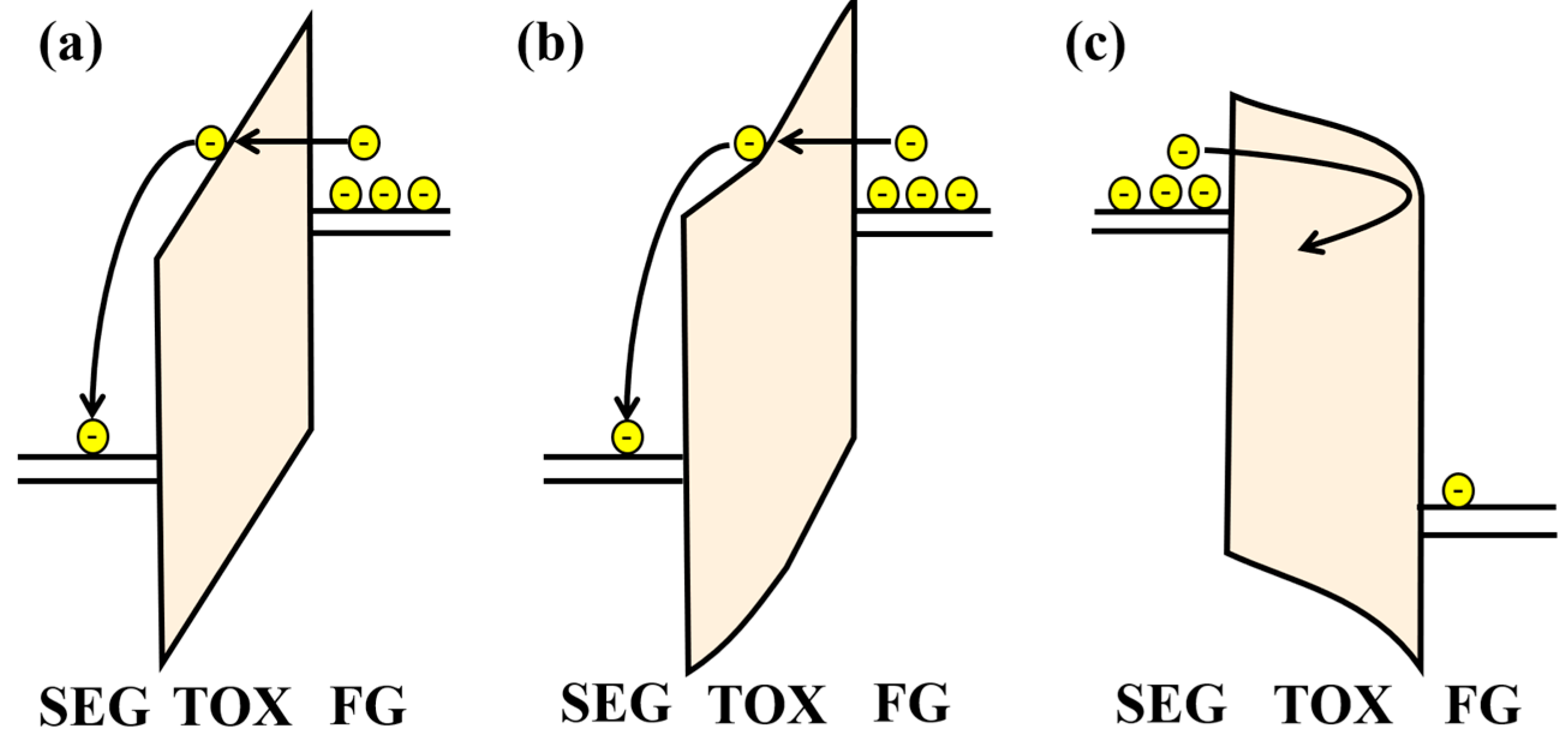
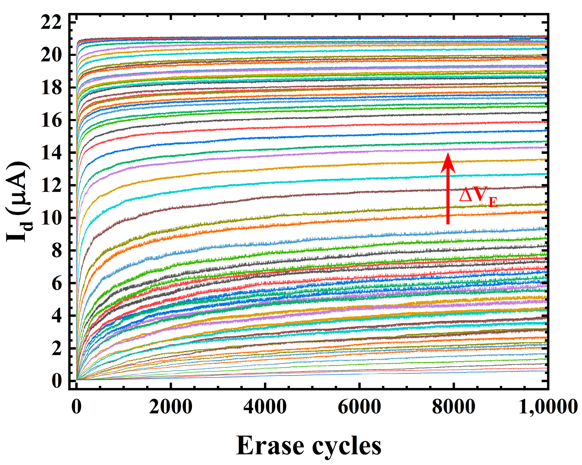
2. Physical Characterization Analysis

Figure 1 shows the schematic of the PLRAM cell. It is implemented on a 90 nm CMOS technology platform [16]. PLRAM uses separated sidewall tunneling oxide (TOX); the electron tunnels between the select erase gate (SEG) and the floating gate (FG) via Fowler–Nordheim (F-N) tunneling. By decoupling the gate oxide and TOX, the degradation probability of the oxide during programming and erasing is reduced, and PLRAM also enables the precise control of electrons. Therefore, PLRAM exhibits enhanced transistor reliability and provides considerable synaptic weights. There are two tunneling directions: direction A is the side wall direction and direction B is the corner direction. The tunneling efficiency is identical between programming and erasing in direction A at a given bias since the distribution of the electric field is uniform, see Figure 2a. On the other hand, direction B gains dense electric field distribution due to the effect of point discharge, and the energy band diagram of the tip closed to the floating gate (FG) is steeper when erasing, as shown in Figure 2b. The electron can easily tunnel from FG to SEG. In contrast, the energy band at the corner closed to SEG makes it hard to form a triangular potential barrier during programming, as shown in Figure 2c. The erase efficiency in PLRAM cells will be significantly larger than the programming efficiency under the same condition because of the corner-enhanced poly-to-poly tunneling effect [20].
Figure 3 demonstrates the single-direction program/erase scan in 1805 PLRAM cells. The programming voltage is much larger than the erasing voltage, as summarized in the inset; however, the erase efficiency is still twice as fast as that of the programming. It implies that applying erase operation to weight tuning can realize higher speed.
As depicted in Figure 4a, the electric field in the TOX ( E F N ) is composed of the intrinsic electric field of the electron charge ( E i ) in the floating gate and the external electric field ( E e x ). The initial E F N is large enough to form a steep triangular barrier in the TOX, giving rise to considerable tunneling current density according to the F-N tunneling formula [21].
J F N = q 3 E 2 8 π h Φ e 4 ( 2 m ) 1 / 2 Φ 3 / 2 3 q E
where represents the reduced Planck constant, q   is the charge quantity, E is the electric field strength, Φ is the barrier height, and m is the mass of the free electron. A large number of electrons tunnel from FG to SEG, and the threshold voltage decreases rapidly, corresponding to the fast part. The reduction in the number of electrons in the FG leads to the lower E i , further resulting in the diminished E F N . The triangular barrier tends to be flat and J F N becomes insignificant, during which time, the slow stage is formed, shown in Figure 4b. Thus, F-N tunneling changes into direct tunneling when E i is down to the critical threshold. It is hard for electrons to tunnel from FG into SEG, consistent with the cut-off stage, shown in Figure 4c.
Figure 5 presents the drain current ( I d ) as a function of erase cycles for different erasing voltages ( V E ) in the PLRAM array. The I d shows an initial sharp rise, and then a gentle change, and each finally stays almost constant. It illustrates the one-to-one mapping between the erase voltage of PLRAM cells and the tuning results by adopting appropriate erase pulses. Therefore, PLRAM can achieve a self-calibrating erase operation with fewer verification steps.

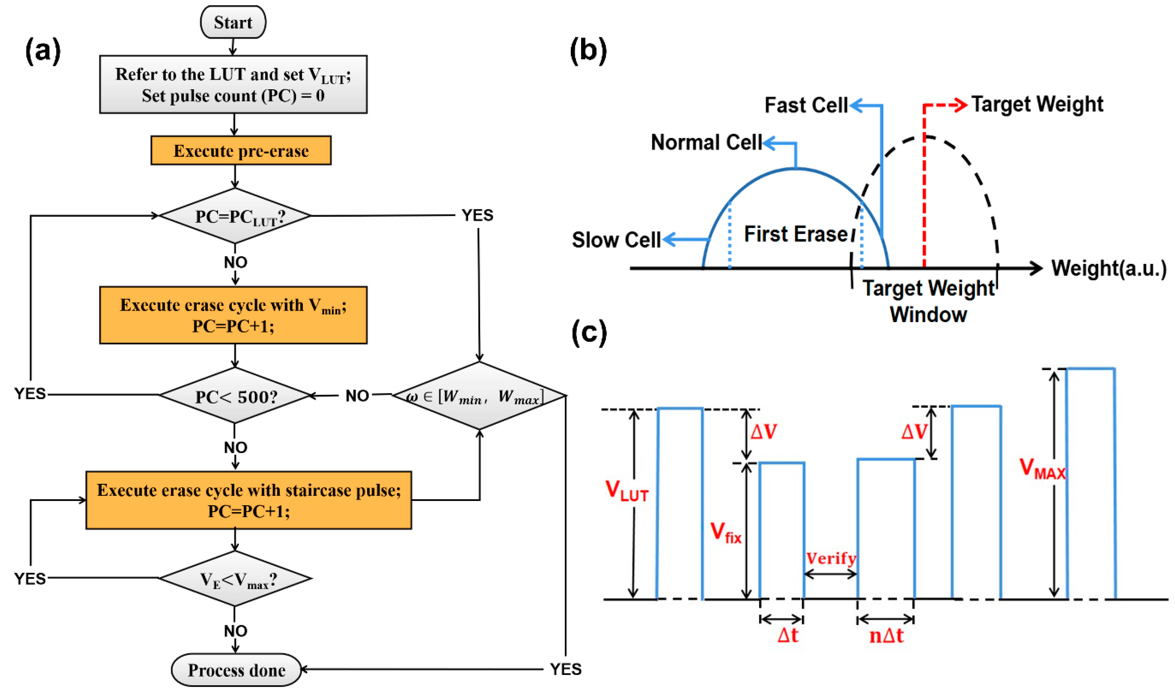
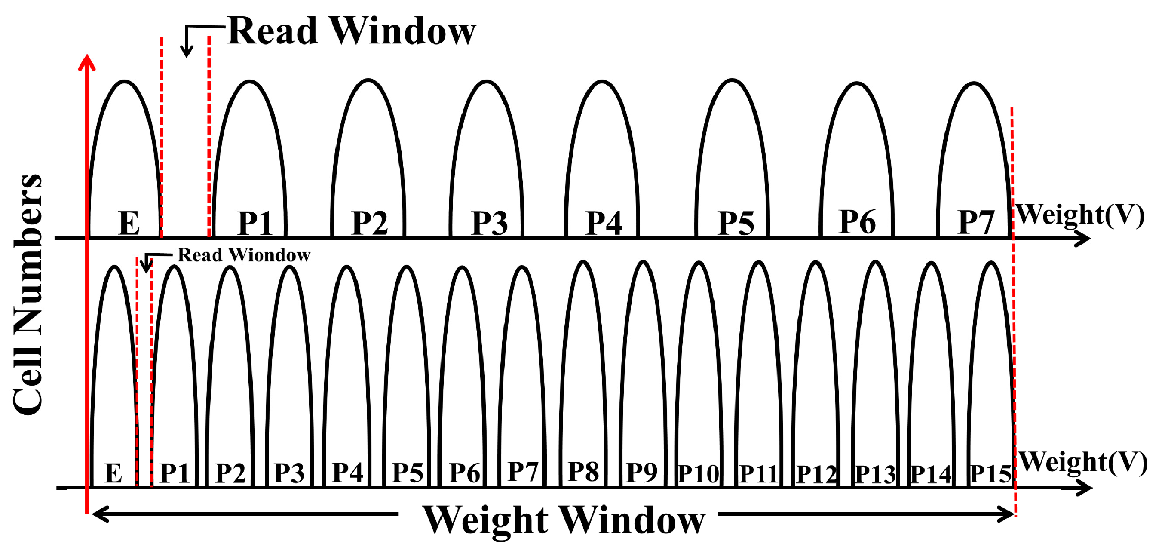
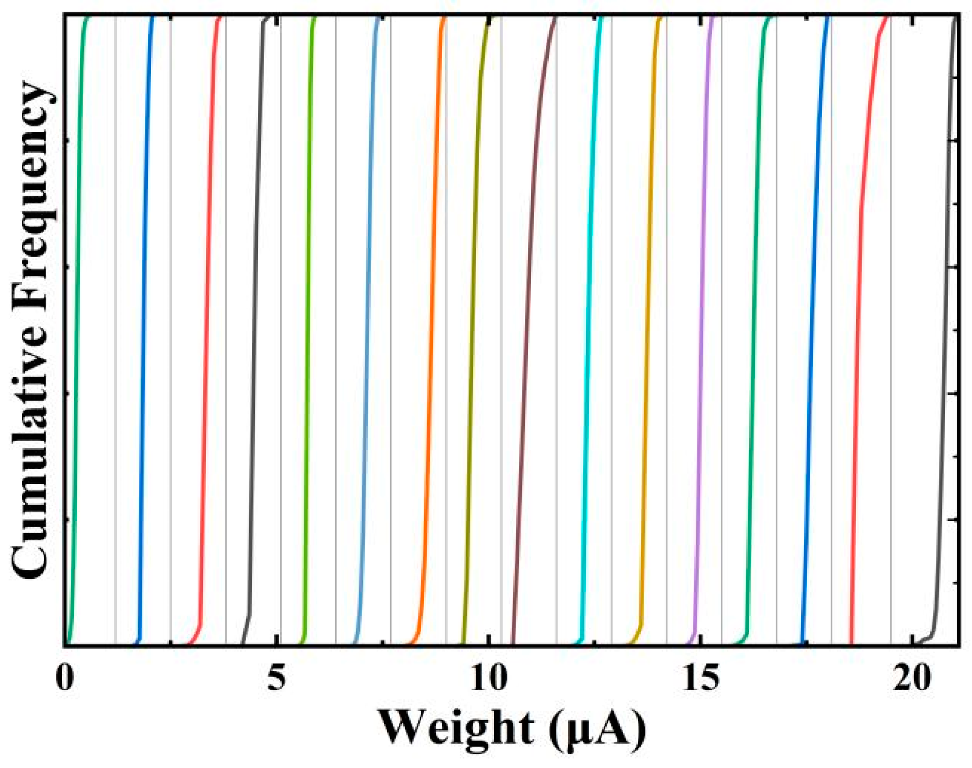
3. Algorithm and Verification

Figure 6a exhibits a fast weight control strategy based on the self-calibrating erase operation in PLRAM. The scheme mainly contains three steps. The first step is the pre-erase operation, and the erase voltage V L U T is loaded according to the look-up table (LUT). All the cells are divided into the fast cells, the normal cells, and the slow cells, respectively, according to the threshold voltage distribution after the pre-erase, shown in Figure 6b. The second step is the erase cycle with fixed bias ( V f i x ) to guarantee fast cells are non-over-erased. The third step is the erase cycle with the increment step pulse program (ISPP) [22] but the cells are only verified at specific cycle times ( P C L U T ) to make slow cells reach the target window quickly and lower the verification times, shown in Figure 6c.
In order to verify the strategy, a QLC mode test is performed on the PLRAM array. The PLRAM cells are divided into 16 weight windows, and the array cells are adjusted to the target weight, in turn, to verify the efficiency and accuracy of the strategy, as schematically shown in Figure 7. QLC mode has higher storage density at the cost of a smaller memory window compared with the triple-level-cell (TLC, 3-bit/cell).
Figure 8a depicts the weight change process of the worst case in the test, and each curve represents a verification step. The weight distribution reaches the target window after 800 pulses, during which, only 4.9 ms for erase and 10 verification steps are taken. The efficiency of weight tuning in the PLRAM array utilized in our strategy is improved by 51%, and the number of verification steps is significantly reduced, shown in Figure 8b. Table 1 illustrates the comparison between this work and some reported algorithms utilized in the QLC, and our strategy achieves the minimum verification steps. It is confirmed that the time cost of the verification will be sufficiently decreased by adopting the self-calibrating erase operation in the weight tunning. The cumulative distribution function of 4-bit weights is presented in Figure 9. Steep and distinct distribution functions are obtained in each target weight window, indicative of the efficient and accurate weight control.

4. Conclusions

In summary, we have demonstrated a fast weight control strategy for PLRAM based on the self-calibrating erase operation through enhanced F-N tunneling. It achieves a 4.9 ms erase process and only 10 verification steps in the worst case. The efficiency is improved by 51% compared with the current strategy. It is attributed to the corner-enhanced poly-to-poly tunneling effect that occurs in the erase process of PLRAM. These findings provide a solution to low efficiency during the tuning process of the PLRAM array and show that our PLRAM has great potential in the application of multi-level memory.

Author Contributions

Conceptualization, Y.L (Yanfei Li). and W.L.; methodology, Y.L (Yanfei Li). and W.L.; software, Y.L (Yanfei Li).; validation, Y.L. (Yanfei Li) and Y.L. (Yinchi Liu); formal analysis, Y.L. (Yanfei Li), B.Z., X.W. and S.D.; investigation, Y.L. (Yanfei Li) and X.Z.; resources, Y.L. (Yanfei Li) and J.Y.; data curation, Y.L. (Yanfei Li) and Z.L.; writing—original draft preparation, Y.L. (Yanfei Li); writing—review and editing, Y.L. (Yanfei Li) and W.L.; visualization, Y.L. (Yanfei Li) and Y.M.; supervision, W.Y.; project administration, Y.L. (Yanfei Li) and W.L.; funding acquisition, W.L. All authors have read and agreed to the published version of the manuscript.

Funding

This research was funded by the National Key R&D Program of China under Grant No. 2021YFB3202500.

Data Availability Statement

Not applicable.

Acknowledgments

The authors would like to thank Cimang Lu, Flash Billion Semiconductor Co., Ltd., Shanghai, China, for constructive mentorship and for providing the devices and platform used in this work.

Conflicts of Interest

The authors declare no conflict of interest.

References

  1. Qureshi, Z.; Mailthody, V.S.; Min, S.W.; Chung, I.-H.; Xiong, J.; Hwu, W. Tearing down the memory wall. arXiv 2020, arXiv:2008.10169. [Google Scholar]
  2. Wulf, W.A.; McKee, S.A. Hitting the Memory Wall: Implications of the Obvious. ACM Sigarch Comput. Archit. News 1995, 23, 20–24. [Google Scholar] [CrossRef]
  3. Ielmini, D.; Wong, H.-S.P. In-memory computing with resistive switching devices. Nat. Electron. 2018, 1, 333–343. [Google Scholar] [CrossRef]
  4. Chen, Y.H.; Krishna, T.; Emer, J.S.; Sze, V. Eyeriss: An Energy-Efficient Reconfigurable Accelerator for Deep Convolutional Neural Networks. IEEE J. Solid-State Circuits 2017, 52, 127–138. [Google Scholar] [CrossRef]
  5. Jouppi, N.P.; Young, C.; Patil, N.; Patterson, D.; Agrawal, G.; Bajwa, R.; Bates, S.; Bhatia, S.; Boden, N.; Borchers, A.; et al. In-Datacenter Performance Analysis of a Tensor Processing Unit. In Proceedings of the 44th Annual International Symposium on Computer Architecture, Toronto, ON, Canada, 14–28 June 2017; pp. 1–12. [Google Scholar] [CrossRef]
  6. Pawlowski, J.T. Hybrid Memory Cube (HMC). In Proceedings of the 2011 IEEE Hot Chips 23 Symposium (HCS), Stanford, CA, USA, 17–19 August 2011; pp. 1–24. [Google Scholar] [CrossRef]
  7. Lee, D.U.; Kim, K.W.; Kim, K.W.; Kim, H.; Kim, J.Y.; Park, Y.J.; Kim, J.H.; Kim, D.S.; Park, H.B.; Shin, J.W.; et al. 25.2 A 1.2V 8Gb 8-channel 128GB/s high-bandwidth memory (HBM) stacked DRAM with effective microbump I/O test methods using 29nm process and TSV. In Proceedings of the 2014 IEEE International Solid-State Circuits Conference Digest of Technical Papers (ISSCC), San Francisco, CA, USA, 9–13 February 2014; pp. 432–433. [Google Scholar] [CrossRef]
  8. Di Ventra, M.; Pershin, Y.V. The parallel approach. Nat. Phys. 2013, 9, 200–202. [Google Scholar] [CrossRef]
  9. Indiveri, G.; Liu, S.C. Memory and Information Processing in Neuromorphic Systems. Proc. IEEE 2018, 103, 1379–1397. [Google Scholar] [CrossRef]
  10. Zhang, X.; Wang, W.; Liu, Q.; Zhao, X.; Wei, J.; Cao, R.; Yao, Z.; Zhu, X.; Zhang, F.; Lv, H.; et al. An Artificial Neuron Based on a Threshold Switching Memristor. IEEE Electron Device Lett. 2017, 39, 308–311. [Google Scholar] [CrossRef]
  11. Luo, Q.; Xu, X.; Gong, T.; Lv, H.; Dong, D.; Ma, H.; Yuan, P.; Gao, J.; Liu, J.; Yu, Z.; et al. 8-layers 3D Vertical RRAM with Excellent Scalability towards Storage Class Memory Applications. In Proceedings of the IEEE International Electron Devices Meeting (IEDM), San Francisco, CA, USA, 2–6 December 2017; pp. 2.7.1–2.7.4. [Google Scholar] [CrossRef]
  12. Shin, J.H.; Jeong, Y.J.; Zidan, M.A.; Wang, Q.; Lu, W.D. Hardware Acceleration of Simulated Annealing of Spin Glass by RRAM Crossbar Array. In Proceedings of the 2018 IEEE International Electron Devices Meeting (IEDM), San Francisco, CA, USA, 1–5 December 2018; pp. 3.3.1–3.3.4. [Google Scholar] [CrossRef]
  13. Narayanan, P.; Burr, G.W.; Virwani, K.; Kurdi, B.N. Circuit-Level Benchmarking of Access Devices for Resistive Nonvolatile Memory Arrays. IEEE J. Emerg. Sel. Top. Circuits Syst. 2016, 6, 330–338. [Google Scholar] [CrossRef]
  14. Ambrogio, S.; Narayanan, P.; Tsai, H.; Shelby, R.M.; Boybat, I.; di Nolfo, C.; Sidler, S.; Giordano, M.; Bodini, M.; Farinha, N.C.P.; et al. Equivalent-accuracy accelerated neural-network training using analogue memory. Nature 2018, 558, 60–67. [Google Scholar] [CrossRef] [PubMed]
  15. Tsai, H.; Ambrogio, S.; Mackin, C.; Narayanan, P.; Shelby, R.M.; Rocki, K.; Chen, A.; Bur, G.W. Inference of Long-Short Term Memory Networks at Software-Equivalent Accuracy Using 2.5 M analog Phase Change Memory Devices. In Proceedings of the 2019 Symposium on VLSI Technology, Kyoto, Japan, 9–14 June 2019; pp. T82–T83. [Google Scholar] [CrossRef]
  16. Gao, S.; Hu, J.; Xiao, J.; Zhang, B. Programmable Linear RAM: A New Flash Memory-based Memristor for Artificial Synapses and Its Application to Speech Recognition System. In Proceedings of the 2019 IEEE International Electron Devices Meeting (IEDM), San Francisco, CA, USA, 7–11 December 2019; pp. 14.1.1–14.1.4. [Google Scholar] [CrossRef]
  17. Zhao, L.; Gao, S.; Zhang, S.; Qiu, X.; Yang, F.; Li, J.; Chen, Z.; Zhao, Y. Neural network acceleration and voice recognition with a flash-based in-memory computing SoC. In Proceedings of the 2021 IEEE 3rd International Conference on Artificial Intelligence Circuits and Systems (AICAS), Washington, DC, USA, 6–9 June 2021; pp. 1–5. [Google Scholar] [CrossRef]
  18. Ricco, B.; Torelli, G.; Lanzoni, M.; Manstretta, A.; Maes, H.E.; Montanari, D.; Modelli, A. Nonvolatile multilevel memories for digital applications. Proc. IEEE 1998, 86, 2399–2423. [Google Scholar] [CrossRef]
  19. Gao, S.; Cong, Y.; Zhang, Z.; Qiu, X.; Lee, C.; Zhao, Y. Superior Data Retention of Programmable Linear RAM (PLRAM) for Compute-in-Memory Application. In Proceedings of the 2020 IEEE International Reliability Physics Symposium (IRPS), Dallas, TX, USA, 28 April–30 May 2020; pp. 1–5. [Google Scholar] [CrossRef]
  20. Tkachev, Y.; Liu, X.; Kotov, A. Floating-Gate Corner-Enhanced Poly-to-Poly Tunneling in Split-Gate Flash Memory Cells. IEEE Trans. Electron Devices 2011, 59, 5–11. [Google Scholar] [CrossRef]
  21. Lenzlinger, M.; Snow, E.H. Fowler-Nordheim Tunneling into Thermally Grown SiO2. J. Appl. Phys. 1969, 40, 278–283. [Google Scholar] [CrossRef]
  22. Hemink, G.J.; Tanaka, T.; Endoh, T.; Aritome, S.; Shirota, R. Fast and accurate programming method for multi-level NAND EEPROMs. In Proceedings of the 1995 Symposium on VLSI Technology, Kyoto, Japan, 6–8 June 1995; pp. 129–130. [Google Scholar] [CrossRef]
  23. Shibata, N.; Maejima, H.; Isobe, K.; Iwasa, K.; Nakagawa, M.; Fujiu, M.; Shimizu, T.; Honma, M.; Hoshi, S.; Kawaai, T.; et al. A 70 nnm 16 Gb 16-level-cell NAND Flash Memory. In Proceedings of the 2007 IEEE Symposium on VLSI Circuits, Kyoto, Japan, 14–16 June 2007; pp. 190–191. [Google Scholar] [CrossRef]
  24. Trinh, C.; Shibata, N.; Nakano, T.; Ogawa, M. A 5.6 MB/s 64 Gb 4b/Cell NAND Flash memory in 43 nm CMOS. In Proceedings of the 2009 IEEE International Solid-State Circuits Conference-Digest of Technical Papers, San Francisco, CA, USA, 8–12 February 2009; pp. 246–247. [Google Scholar] [CrossRef]
  25. Shibata, N.; Kanda, K.; Shimizu, T.; Nakai, J.; Nagao, O.; Kobayashi, N.; Miakashi, M.; Nagadomi, Y.; Nakano, T.; Kawabe, T.; et al. A 1.33-Tb 4-Bit/Cell 3-D Flash Memory on a 96-Word-Line-Layer Technology. IEEE J. Solid-State Circuits 2020, 55, 178–188. [Google Scholar] [CrossRef]
  26. Feng, Y.; Zhang, D.; Zhao, G.; Sun, Z.; Bai, M.; Qi, Y.; Gong, X.; Liu, J.; Zhang, J.; Wu, J.; et al. A Novel Array Programming Scheme for Large Matrix Processing in Flash-Based Computing-in-Memory (CIM) with Ultrahigh Bit Density. IEEE Trans. Electron Devices 2023, 70, 461–467. [Google Scholar] [CrossRef]
Figure 1. The schematic of PLRAM.
Electronics 12 03466 g001
Figure 2. Energy band diagram in the different F-N tunneling directions: (a) The side wall direction. (b) The corner direction of erasing. (c) The corner direction of programming.
Electronics 12 03466 g002
Figure 3. The single-direction program/erase in 1805 PLRAM cells. The transparent gray background is the total weights, and the red line shows the average result. The operating condition is digested in the inset.
Electronics 12 03466 g003
Figure 4. The energy band diagram in the erase process: (a) Fast stage. (b) Slow stage. (c) Cut-off stage. Red dashed lines represent the change of energy band diagram.
Electronics 12 03466 g004
Figure 5. I d curves with different V E in the PLRAM array. Different-colored lines represent distinct V E and the red arrow indicates the growth direction.
Electronics 12 03466 g005
Figure 6. (a) The scheme of the fast weight control strategy based on the self-calibrating erase operation in PLRAM. (b) The schematic of pre-erase operation. (c) The pulse of the strategy.
Electronics 12 03466 g006
Figure 7. Weight windows for TLC and QLC in PLRAM.
Electronics 12 03466 g007
Figure 8. (a) The weight change process of the worst case in QLC. (b) The comparison of process time between the current strategy and this work.
Electronics 12 03466 g008
Figure 9. The cumulative frequency of PLRAM array after the 4-bit weights test. The weight distribution in each target window is shown as curves of different colors.
Electronics 12 03466 g009
Table 1. The comparison between this work and some reported algorithms applied in the QLC. IPNPP represents the incremental positive–negative step pulse programming.
ReferencesThis Work16-16 Two-Step Programming [23]Three-Step Programming [24]8-16 Two-Step Programming [25]IPNPP [26]
CircuitNORNANDNANDNANDNOR
Process 90 nm70 nm43 nmBiCS 55 nm
Verification steps10555About 600About 45515
Disclaimer/Publisher’s Note: The statements, opinions and data contained in all publications are solely those of the individual author(s) and contributor(s) and not of MDPI and/or the editor(s). MDPI and/or the editor(s) disclaim responsibility for any injury to people or property resulting from any ideas, methods, instructions or products referred to in the content.

