1. Introduction
With the development of modern electronic devices, DC-DC converters have gradually become essential power conversion devices. DC-DC converters have a wide range of applications in various fields, such as energy conversion, electric vehicles, electric aircraft [
1,
2], renewable energy systems, electronic devices and communication equipment. They play a vital role in ensuring stable power voltage and facilitating efficient energy conversion. In fuel-cell-powered electric vehicles, the role of the DC-DC converter is crucial. It adjusts the voltage level and stability to ensure that the output voltage of the fuel cell is suitable for supplying the electric motor drive. This ensures that the power system of the electric vehicle operates reliably and stably, providing the required power output. Through these DC-DC converters, the soft output characteristics and unstable output voltage of the fuel cell can be effectively converted and adjusted to meet the stable voltage requirements of the motor drive. This adjustment and conversion ensure that the power system of the electric vehicle operates normally in various conditions, providing smooth and reliable power output. DC-DC converters are electronic devices that play a crucial role in electronic systems. They are capable of converting the input voltage from the power source to a voltage level suitable for a specific load. Whether there is a need to boost the voltage to meet high power requirements or lower the voltage to accommodate low-power devices, DC-DC converters can effectively fulfill power demands in various application scenarios [
3,
4,
5,
6]. Based on their circuit structures, DC-DC converters can be divided into two categories: isolated converters and non-isolated converters [
7]. Isolated converters have higher hardware costs and larger volumes. Moreover, their efficiency and stability are limited due to some factors such as weight, losses and coupling coefficients when converters are used [
8,
9,
10]. Non-isolated high-gain DC-DC converters hold tremendous potential in the field of power conversion technology. Their strong boosting capability, high efficiency and good adjustability have made them a hot topic in current research, receiving wide attention and applications in various fields. However, non-isolated high-gain DC-DC converters also have some drawbacks. Firstly, they may introduce high input current ripple due to the increased current required for voltage boosting, resulting in increased fluctuations in the input current. Secondly, to achieve the desired functionality, non-isolated high-gain DC-DC converters may require additional components. Additionally, there may be certain limitations in terms of output voltage for non-isolated high-gain DC-DC converters. In conclusion, although non-isolated high-gain DC-DC converters have many advantages, it is also necessary to consider some of their drawbacks. In applications, it is important to consider these factors comprehensively and make choices and create designs based on specific requirements to ensure that the converter can effectively meet the system’s needs.
In subsequent developments, non-isolated DC-DC converters mainly include cascaded converters, coupled inductor converters, switched capacitor converters and switched inductor converters. Cascaded converters refer to the series connection of multiple power converters of different types according to a specific topology [
11,
12]. Cascaded converters have advantages such as expandability, optimized efficiency and optimized control strategies, but they also face challenges of increased complexity, increased cost and volume, system stability and reliability issues [
13,
14,
15,
16,
17,
18]. Coupled inductor converters use multiple coupled inductors to achieve energy conversion, with advantages of high efficiency, high density, reduced current ripple and lower noise. However, they also suffer from drawbacks such as increased complexity, increased cost and limited input voltage range [
19,
20]. Switched capacitor converters have the advantages of a small size and simple design; however, their boost capability is limited, and they have lower efficiency [
21,
22]. Switched inductor converters possess advantages of high efficiency, strong energy storage capability and low noise generation, but they have complex designs and higher costs [
23,
24].
To improve non-isolated converters, ref. [
25] proposed a quadratic buck-boost converter with a wide gain range; however, it has low boost capability and efficiency. One less inductor and capacitor were used in [
26] compared to the proposed converter to achieve high gain. Although the non-isolated DC-DC converters introduced in [
26,
27] have efficient characteristics, their boost capability and efficiency are limited due to their use at an extremely low duty ratio (D ∈ (0.1–0.3)). In practical applications, it is necessary to consider these limitations based on specific requirements and design considerations, and choose appropriate converters to meet the requirements. The authors of [
28] presented an efficient non-isolated converter based on the ZETA converter, which offers a wide gain range. However, compared to some other converters, this non-isolated DC-DC converter may have a slightly lower voltage boosting capability, even though its voltage gain is only 8 at a duty cycle of 0.8.
This paper presents a novel solution called the high-gain wide-range (HG-WR) DC-DC converter, which aims to improve the limitations mentioned earlier, such as the challenges posed by very low duty ratios, low voltage gain, and low efficiency. The HG-WR converter offers significant improvements in these areas. The HG-WR converter is designed using a switch-capacitor topology, where the two branches of the capacitor are separated, and two inductors and one capacitor are used to replace the previous single-inductor structure. Compared to the traditional boost converter and cascaded boost converter, as well as efficient converters such as the IB-CCS-I [
18], IC-CCS-II [
18], IB-CCS-IV [
18] and quadratic buck-boost converter [
25], the HG-WR converter demonstrates superior boost capability and higher efficiency. Moreover, the HG-WR converter exhibits superior performance compared to existing converters in terms of its enhanced availability and extended gain range. This paper focuses on the operating principle of the converter in Continuous Conduction Mode (CCM). It offers an in-depth examination of the voltage and current interdependencies among each component during CCM operation of the converter, and determines the voltage and current loads experienced by each component, thereby assessing the stress levels they endure. The boundary conditions between CCM and Discontinuous Conduction Mode (DCM) were determined, and the parameters of each component were consequently designed to optimize the efficiency of the converter. To validate its performance, the HG-WR converter was compared with other converters and verified through experimental results from simulations and hardware.
2. The Operating Principle of an HG-WR Converter
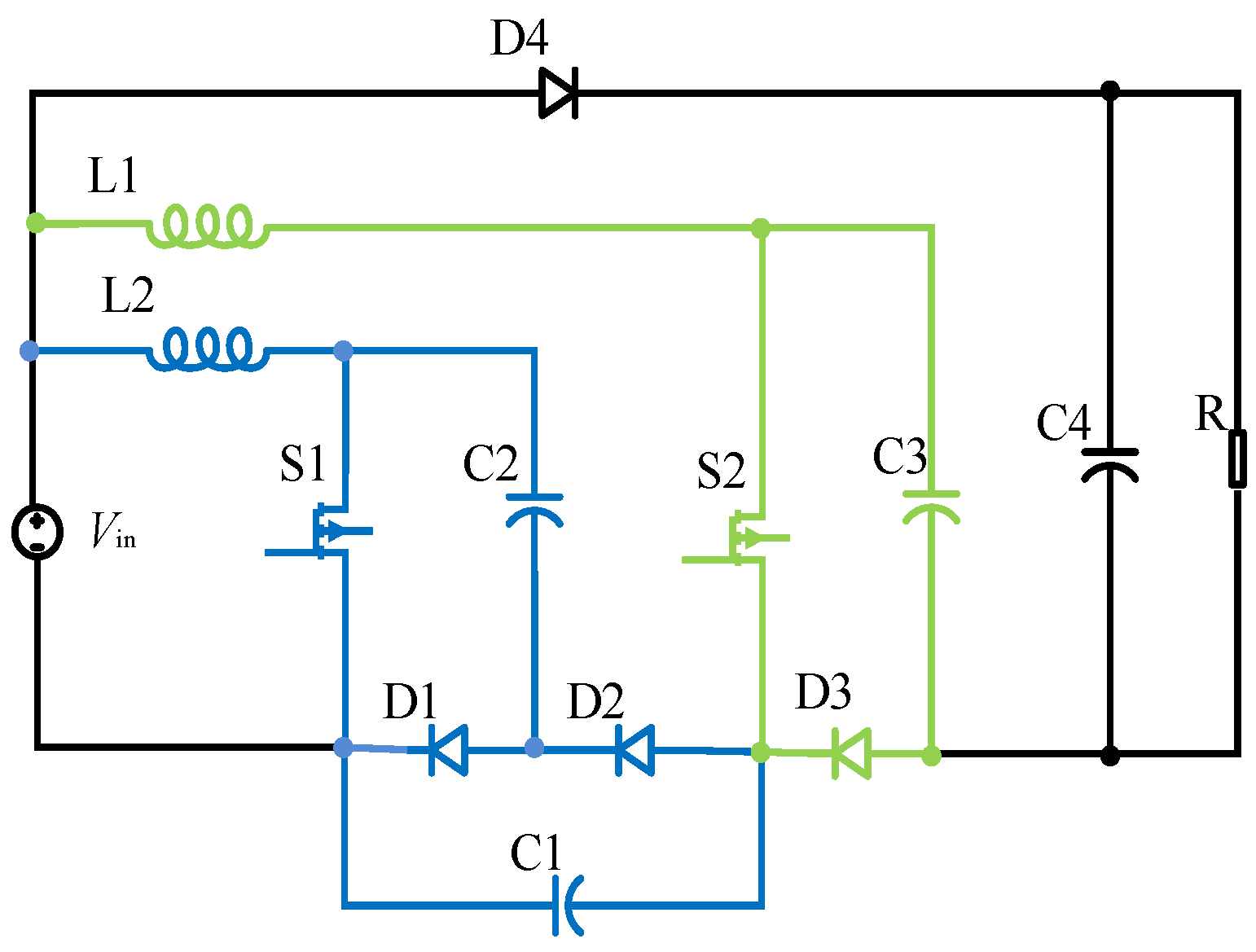
As shown in
Figure 1, the switch-capacitor structure is split into two branches, with the green branch remaining unchanged, while in the blue branch, a new topological structure can be achieved by connecting two capacitors in parallel, and then the HG-WR converter is formed. This system consists of the following components: a DC input source,
Vin; two switches, S1 and S2; two inductors, L1 and L2; four diodes, D1, D2, D3 and D4; and four capacitors, C1, C2, C3 and C4. There is also a load R connected to these components.
In this section, for the purpose of simplifying the analysis of the HG-WR converter, all analyses are based on the following assumptions:
Active switches, inductors, capacitors and diodes are all ideal components. The effects of resistance and voltage drop in power semiconductor devices, as well as parasitic parameters in energy storage components, can be neglected.
Assuming that the inductors and capacitors have sufficiently high values, a stable current through the inductors and a stable voltage across the capacitors are ensured.
The two operating states of the HG-WR converter in CCM are analyzed in detail as follows:
Operating State 1 [t
0, t
1]: During this interval, S1 and S2 are turned on. Diodes D1 and D3 are biased in reverse direction, while D2 and D4 are biased in the forward direction. In the green loop, the DC input source
Vin and capacitor C2 are connected in series, and they charge inductor L1 through switches S1, S2 and diode D2. At the same time, in the red loop, the DC input source
Vin charges inductor L2 through switch S1. In the orange loop, capacitor C2 supplies charge to capacitor C1 through the conduction of diode D2 and the activation of switch S1. In the blue loop, the DC input source
Vin and capacitors C2 and C3 are connected in series, and they power the load through switches S1, S2 and diode D2. The equivalent circuit is illustrated in
Figure 2a. By applying Kirchhoff’s Voltage Law (KVL), Equation (1) is derived, where
VC2 and
VC3 represent the voltages across the capacitors C2 and C3, respectively.
VL1 and
VL2 denote the voltage drop across inductors L1 and L2, respectively, while
Vo represents the voltage generated at the output.
Operating State 2 [t
1, t
2]: During this interval, S1 and S2 are turned off. The diode states are opposite to State 1. In blue loop, the DC input source
Vin is connected in series with inductor L1 and capacitor C1. The charging of capacitor C3 is achieved by passing current through diode D3 from the combination above. In the green loop, the DC input sources
Vin are connected to the inductor L2 in series and charge the capacitor C2 through diode D1, and in the orange loop, C4 supplies the load R. The equivalent circuit in this state can be represented as shown in
Figure 2b. By applying KVL, Equation (2) can be obtained. The voltage drops across capacitors C1 and C4 are considered
VC1 and
VC4, respectively.
Based on the principle of flux balance for inductors and the principle of charge balance for capacitors, Equation (3) can be derived, where D represents the duty ratio.
By applying Equations (1)–(3), the relationship between the input voltage
Vin and the output signal voltage
Vo can be obtained, which represents the voltage gain G of the HG-WR converter.
According to the previous analysis, the HG-WR converter in CCM exhibits a series of main waveforms, which are illustrated in
Figure 3. Where, PWM represents the control signal for switches S1 and S2. The time interval DT, (1-D)T represent the switches turning on and off, respectively, and T represents one period.
iL1 and
iL2 denote the currents passing through inductors L1 and L2, respectively.
3. Analysis of Component Voltage Stress
When switches S1 and S2 are turned off, the voltage stress on switches S1 and S2 can be expressed as Equation (5), where
VS1 and
VS2 represent the voltages stress on switches S1 and S2, respectively.
By combining Equations (3) and (5), the voltage stress experienced by switches S1 and S2 can be determined as follows:
When diodes are reverse-biased, the voltage stresses can be expressed as Equation (7), where
VD1,
VD2,
VD3 and
VD4 represent the voltages stress on diodes D1, D2, D3 and D4, respectively.
4. Component Current Stress Analysis
In accordance with the principle of charge balance in capacitors, the average current passing through a capacitor during one complete period (T) is zero. Combining this principle with Kirchhoff’s current law (KCL), Equation (8) provides a formula to calculate the average current flowing through capacitors C1-C4.
iC1_on represents the current flowing through the capacitor C1 during DT.
iLi_on,
iLi_off,
i = 1, 2,
iin_on and
iin_off represent the inductor current and input current during DT and (1-D)T, respectively.
IR represents the current flowing through the load.
Assuming a sufficiently high switching frequency and large inductance value, with continuous current pass through the inductor, Equation (9) provides a means to represent the average current that passes through the inductor, denoted as
IL.
By substituting Equation (8) into Equation (9), the average currents flowing through the inductor over one period can be obtained, as shown in Equation (10).
By referring to Equation (11), the currents flowing through switches S1 and S2 when they are in the “on” state can be calculated. These currents are denoted as
iS1 and
iS2 respectively.
The currents flowing through D2 and D4 when the switches S1 and S2 are in the “off” states are shown in Equation (12), where
iD2 and
iD4 represent the currents flowing through diodes D2 and D4, respectively.
Equation (13) provides a means to calculate the currents passing through diodes D1 and D3 when switches S1 and S2 are turned on. The currents through D1 and D3 are represented by
iD1 and
iD3, respectively.
The average currents flowing through the switches and diodes over one period can be expressed as Equation (14).
5. Design Considerations
5.1. Inductor Design
When the switches are turned on, both inductor L1 and L2 are subject to the following differential equation:
In Equation (15), ∆i
L represents the current ripple through the inductor. If the current ripple is large, it will subject the switches to significant current stress. Therefore, to protect the switches, it is necessary to limit the current ripple within a reasonable range for the inductor. The magnitude of the current ripple can be expressed using the ripple coefficient
x_{L,%}, and ∆i
L must satisfy Equation (16).
According to Equation (16), the inductance coefficients of L1 and L2 can be obtained as Equation (17), where the inductance coefficients of
L1 and
L2 represent the inductance values of L1 and L2, respectively.
To ensure the stability and reliability of the HG-WR converter in CCM, it is necessary to satisfy the following inequalities to limit the average inductor current
IL and current ripple ∆i
L:
Thus, according to Equations (17) and (18), Equation (19) is given as:
By substituting Equations (3) and (10) into Equation (19), the specific value of inductance can be determined via Equation (20), where
fs represents the switching frequency.
By analyzing the load current, inductance value and operating parameters of the HG-WR converter, the boundary between CCM and DCM can be determined.
The relationship between K and duty ratio is plotted in
Figure 4. It can be seen that the CCM region is above the curve, while the DCM region is the area below the curve.
5.2. Capacitor Parameter Design
The capacitor allows the circuit to achieve a higher voltage gain by undergoing periodic charging and discharging. During one period, the capacitor generates a certain voltage ripple ∆v
C. To obtain better output voltage characteristics, the ripple coefficient
x_{
C,%} is introduced, where ∆v
C =
x_{
C,%}
VC. The capacitor satisfies the following differential equation:
where
IC_off represents the current flowing through the capacitor during (1-D)T. During one period, the currents flowing through capacitors C1, C2, C3 and C4 can be represented by Equation (23):
By substituting Equation (22) into Equation (23), capacitors can be obtained in Equation (24), where
fs represents the switching frequency.
6. Efficiency Calculation
In this section, detailed calculations that determine the power losses in the switch, diode, inductor, and capacitor are described, and the conversion efficiency of the HG-WR converter is derived. Firstly, the conduction and switching losses in the switch are considered. The conduction loss is caused by the resistance during the switch’s on-state, while the switching loss is the power dissipated during the switch’s off-state. Next, the forward losses in the diode are analyzed. The forward loss is the power dissipated due to the product of the forward voltage and current in the diode. Then, the losses in the inductor are taken into account. The losses in the inductor are primarily caused by the resistance of the inductor’s current and the hysteresis loss in the magnetic core. Lastly, the losses in the capacitor are analyzed. The losses in the capacitor are mainly due to the power dissipated by the equivalent series resistance of the capacitor. By calculating and analyzing these power losses, the total power loss in the HG-WR converter is determined. Then, by comparing the total output power with the total input power, the conversion efficiency of the HG-WR converter is obtained.
The power loss of a switch can be divided into two parts: switch loss and conduction loss, and their expressions are given in Equation (25).
where
PS,
PSW and
PrS represent the total power loss, switching loss and conduction loss, respectively. The switch loss can be expressed using Equation (26).
where
tr and
tf represent the delay times during the turn-on state and turn-off state, respectively. Their values are 16 ns and 6 ns respectively.
fs represents the switching frequency, and its value is 100 kHz. The total switch loss
PSW is represented by Equation (27).
ISk(rms) (k = 1, 2) represents the effective current flowing through the switch during one period, as shown in Equation (28).
In Equation (28),
iSk_on and
iSk_off represent the switch current during DT and (1-D)T, respectively. Therefore, the conduction loss of the switch can be expressed by Equation (29).
where
rSk represents the internal resistance of the switch. The expression for the conduction loss of the switch can be deduced and is shown in Equation (30).
The loss of the diode is expressed by Equation (31), where
VF denotes the voltage across the diode when it is forward biased, and
IDi is the average current flowing through the diode.
PVF denotes the amount of power that is lost or dissipated as heat in the diodes.
Equation (32) can be used to describe and calculate the effective currents passing through the inductors L1 and L2.
IL(rms) represents the effective current flowing through the inductor.
Equation (33) presents a way to quantify the conduction losses occurring in inductors L1 and L2. The internal resistances of inductors L1 and L2 are denoted by
rL1 and
rL2, respectively.
The total conduction loss of the inductors can be calculated by summing the individual conduction losses of each inductor.
By using Equation (35), the amount of energy dissipated as heat in the capacitors due to conduction can be determined and quantified.
ICK(rms) (k = 1, 2) represents the effective current flowing through the capacitor, and the effective current for each capacitor is given by Equation (36).
Then, the total conduction loss of the capacitors can be expressed by Equation (37), where
rC represents the internal resistance of the capacitor.
This method can be used to evaluate and quantify the efficiency of other types of DC-DC converters. By considering the energy losses between input power and output power, this method can be used to compare and analyze the efficiency of different types of DC-DC converters.
When
Vin = 5 V, D = 0.5 and R = 100 Ω, according to the parameters of each component, the efficiency of the HG-WR converter is 92.08%. The power loss pie chart is shown in
Figure 5. The power loss ratio of each component can be inferred from the information presented in
Figure 5. The inductors have the smallest loss, accounting for 0.58% of the total loss. The diodes have the highest loss, accounting for 41.40% of the total loss.
7. Comparative Analysis of Performance
To validate the high-gain characteristics of the HG-WR converter, in this section, a comparison is made between the boost, quadratic boost, IB-CCS-I [
18], IC-CCS-II [
18], IB-CCS-IV [
18], quadratic buck-boost [
25] and proposed converters. The gain comparison curve is shown in
Figure 6.
By examining
Figure 6, it becomes apparent that the proposed converter demonstrates a considerably higher voltage gain when operating under the same duty ratio.
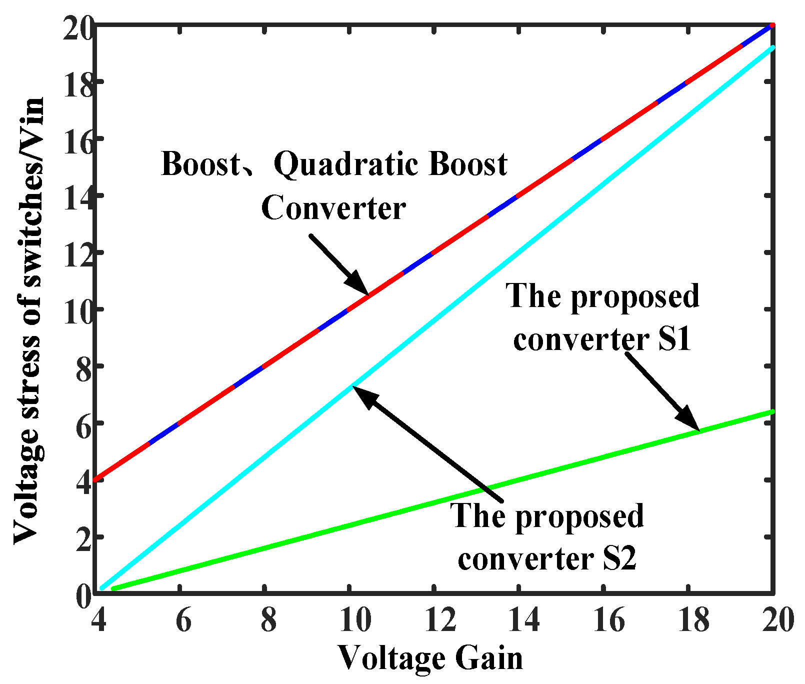
Figure 7 illustrates the variation in switch voltage stress with voltage gain for the proposed converter. In order to better demonstrate the magnitude of the switch voltage stress of the proposed converter, a boost converter and quadratic boost converter are included for comparison. It is evident that the proposed converter effectively mitigates the switching voltage stress, resulting in a significant reduction compared to the two conventional DC-DC converters.
From
Figure 7, it can be observed that the proposed converter exhibits lower switch stress for the same voltage gain when comparing the efficiency of the proposed converter with the NHS converter [
7] at D values of 0.2 to 0.5. The efficiency comparison between the proposed converter and the NHS converter is shown in
Figure 8.
The efficiency comparison curve of the HG-WR converter and the NHS converter for D = 0.2~0.5 is shown in
Figure 8. The HG-WR converter, which has one more switch and capacitor compared to the NHS converter, clearly exhibits a higher efficiency than the NHS converter in the range of 0.2 to 0.5, as is evident from
Figure 8. The converter achieves the highest efficiency when the duty cycle D is set to 0.4. This efficiency value is significantly better than what is achieved at other duty cycles.
Based on the comparative analysis, it can be concluded that this converter outperforms existing DC-DC converters in terms of voltage gain. This means that the converter is capable of more effectively increasing the level of input voltage, resulting in a higher output voltage. Therefore, for applications that require a higher output voltage, this converter is a more attractive choice. On the other hand, through a comparative analysis, it can be also observed that the proposed converter is capable of reducing switch voltage stress compared to the boost converter and the quadratic boost converter. This means that, under the same operating conditions, the switch components of this converter experience lower voltage stress. As a result, this type of converter may offer better reliability and longevity in practical applications, while reducing the stress on switch components and improving system stability. The efficiency comparison chart clearly shows that the HG-WR converter exhibits a significant improvement in efficiency compared to the NHS converter. This indicates that the HG-WR converter is able to convert electrical energy more effectively and reduce energy losses under the same operating conditions. This improvement may be attributed to the optimized design and control strategies of the HG-WR converter, as well as its higher conversion efficiency. Therefore, from an efficiency perspective, the HG-WR converter is a superior choice.
8. Analysis of Simulation and Experimental Results
To verify the performance characteristics of the proposed converter, both a simulation and an experimental prototype were established. The experimental prototype was constructed using the parameters shown in
Table 1.
A simulation model was developed in Simulink, and the outcomes of the simulation are depicted in
Figure 9.
VS1 and VS2 represent the voltage of switches S1 and S2, respectively. iL1 and iL2 represent the currents flowing through inductors L1 and L2, respectively. PWM represents the control signal for switches S1 and S2. Vin represents the input voltage, while Vo represents the output voltage of the HG-WR converter. VC1, VC2 and VC3 represent the voltages across the capacitors C1, C2 and C3, respectively. It can be observed that the input voltage of the converter is 5 V, the output voltage is 45 V and the voltages across capacitors C1, C2 and C3 are 10 V, 10 V and 30 V, respectively. These values are consistent with the theoretical calculations. This indicates that the converter is operating as expected, with the input voltage being transformed to the desired output voltage.
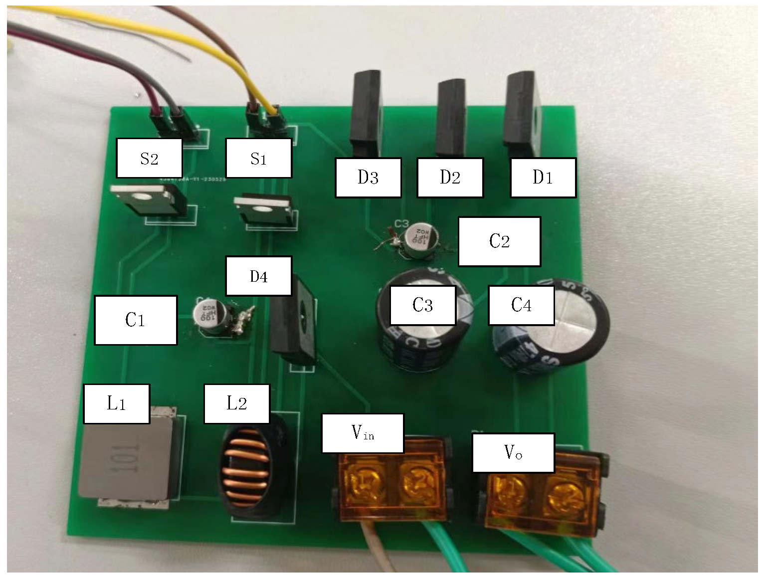
As shown in
Figure 10, the established hardware prototype is based on parameter design.
However, the presence of parasitic resistance in the device causes a slight decrease in the actual value compared to the theoretical value. The experimental results, as depicted in
Figure 11, demonstrate that the proposed converter achieves an output voltage of
Vo = 42.3 V when the input voltage is
Vin = 4.99 V and the duty ratio is 0.5.
VS1 and VS2 represent the voltages across the switches S1 and S2, respectively. Given that Vin is 5 V and D is 0.5, according to Equations (3) and (4), VC1, VC2, VC3 and Vo can be calculated as 10 V, 10 V, 30 V and 45 V, respectively. Due to the forward voltage drop in diodes and the losses in the components, the actual output values of the converter have slight differences from the theoretical values.
9. Conclusions
In this paper, a high-gain DC-DC converter with a wide range of output voltage is proposed. This converter incorporates multiple capacitors, enhancing its energy storage capacity and expanding the range of output voltage. A comprehensive examination was carried out on the voltage and current interdependencies of every component within the converter operating in CCM. The voltage and current loads on each component were calculated, enabling the boundary conditions between CCM and DCM to be determined. Based on these conditions, the parameters of each component were meticulously designed. Additionally, the efficiency of the converter was evaluated through calculations. To validate its performance, comparisons were made between the converter in question and other similar converters, and verification was carried out through simulations and hardware experiments. The results indicate that the HG-WR converter exhibits simultaneous advantages, including a high voltage gain and wide range of output voltage.
Author Contributions
Conceptualization, S.Z. and H.L.; methodology, S.Z., H.L. and X.D.; software, H.L. and S.L.; validation, S.Z., H.L. and J.Z.; formal analysis, S.L.; investigation, P.W.; resources, S.D.; writing—original draft preparation, H.L. and S.D.; writing—review and editing, S.Z. and X.D.; S.Z. and H.L. contributed equally. All authors have read and agreed to the published version of the manuscript.
Funding
This work was financially supported by the S&T Program of Hebei (22352201D), the Open Project of Provincial Collaborative Innovation Center of Industrial Energy-saving and Power Quality Control, Anhui Province (KFKT201504) and the Science Foundation of Hebei Normal University (L2023J03).
Data Availability Statement
Not applicable.
Conflicts of Interest
The authors declare no conflict of interest.
References
- Russo, A.; Cavallo, A. Stability and Control for Buck–Boost Converter for Aeronautic Power Management. Energies 2023, 16, 988. [Google Scholar] [CrossRef]
- Cavallo, A.; Canciello, G.; Russo, A. Buck-Boost Converter Control for Constant Power Loads in Aeronautical Applications. 2018 IEEE. In Proceedings of the Conference on Decision and Control (CDC), Miami Beach, FL, USA, 17–19 December 2018; IEEE: Piscataway, NJ, USA, 2018. [Google Scholar] [CrossRef]
- Mamun, M.A.; Hasan, M.A.; Khan, E. High Voltage Conversion DC-DC Step Up Converter for Fuel Cell Applications. In Proceedings of the 2017 3rd International Conference on Electrical Information and Communication Technology (EICT), Khulna, Bangladesh, 7–9 December 2017. [Google Scholar] [CrossRef]
- Tseng, K.C.; Lin, J.T. High step-up DC/DC converter for fuel cell hybrid electric vehicles. In Proceedings of the IEEE International Symposium on Next-Generation Electronics, Kaohsiung, Taiwan, 25–26 February 2013. [Google Scholar] [CrossRef]
- Krzywinski, G. Integrating Storage and Renewable Energy Sources into a DC Microgrid Using High Gain DC DC Boost Converters. In Proceedings of the 2015 IEEE First International Conference on DC Microgrids (ICDCM), Atlanta, GA, USA, 7–10 June 2015. [Google Scholar] [CrossRef]
- Bascope, R.P.T.; Bezerra, L.D.S.; Branco, C.G.C.; Cruz, C.M.T.; Sousa, G.J.M. A step-Up DC-DC converter for non-isolated on-line UPS applications. In Proceedings of the 2010 IEEE International Symposium on Industrial Electronics, Bari, Italy, 4–7 July 2010. [Google Scholar] [CrossRef]
- Liu, L.; Li, D.; Yao, L. A family of non-isolated transformerless high step-up DC-DC converters. Int. Trans. Electr. Energy Syst. 2019, 29, e2794. [Google Scholar] [CrossRef]
- Lee, J.-H.; Liang, T.-J.; Chen, J.-F. Isolated Coupled-Inductor-Integrated DC–DC Converter with Nondissipative Snubber for Solar Energy Applications. IEEE Trans. Ind. Electron. 2014, 61, 3337–3348. [Google Scholar] [CrossRef]
- Changchien, S.-K.; Liang, T.-J.; Chen, J.-F.; Yang, L.-S. Novel High Step-Up DC–DC Converter for Fuel Cell Energy Conversion System. IEEE Trans. Ind. Electron. 2010, 57, 2007–2017. [Google Scholar] [CrossRef]
- Sharma, R.; Gao, H. Low cost high efficiency DC-DC converter for fuel cell powered auxiliary power unit of a heavy vehicle. IEEE Trans. Power Electron. 2006, 21, 587–591. [Google Scholar] [CrossRef]
- Andrade, A.M.S.S.; Schuch, L.; Martins, M.L.D.S. Analysis and Design of High-Efficiency Hybrid High Step-Up DC–DC Converter for Distributed PV Generation Systems. IEEE Trans. Ind. Electron. 2018, 66, 3860–3868. [Google Scholar] [CrossRef]
- Huber, L.; Jovanovic, M.M. A design approach for server power supplies for netwo. In Proceedings of the IEEE APEC 2000—Applied Power Electronics Conference, New Orleans, LA, USA, 6–10 February 2000. [Google Scholar] [CrossRef]
- Luo, F.L.; Ye, H. Positive output cascade boost converters. IET Electr. Power Appl. 2004, 5, 151. [Google Scholar] [CrossRef]
- Li, H.; Guo, Z.; Ren, F.; Zhang, X.; Zhang, B. A stability analysis method based on Floquet theory for multi-stage DC-DC converters system. In Proceedings of the 2017 IEEE Energy Conversion Congress and Exposition (ECCE), Cincinnati, OH, USA, 1–5 October 2017. [Google Scholar] [CrossRef]
- Andrade, A.M.S.S.; Hey, H.L.; Schuch, L.; Martins, M.L.D.S. Comparative Evaluation of Single Switch High-Voltage Step-Up Topologies Based on Boost and Zeta PWM Cells. IEEE Trans. Ind. Electron. 2017, 65, 2322–2334. [Google Scholar] [CrossRef]
- Siwakoti, Y.P.; Blaabjerg, F. Single Switch Nonisolated Ultra-Step-Up DC–DC Converter with an Integrated Coupled Inductor for High Boost Applications. IEEE Trans. Power Electron. 2017, 32, 8544–8558. [Google Scholar] [CrossRef]
- Stala, R.; Waradzyn, Z.; Penczek, A.; Mondzik, A.; Skala, A. A Switched-Capacitor DC–DC Converter with Variable Number of Voltage Gains and Fault-Tolerant Operation. IEEE Trans. Ind. Electron. 2018, 66, 3435–3445. [Google Scholar] [CrossRef]
- Zeng, Y.; Li, H.; Wang, W.; Zhang, B.; Zheng, T.Q. High-Efficient High-Voltage-Gain Capacitor Clamped DC–DC Converters and Their Construction Method. IEEE Trans. Ind. Electron. 2020, 68, 3992–4003. [Google Scholar] [CrossRef]
- Hwu, K.I.; Yau, Y.T.; Shieh, J.J. High step-up converter based on coupling inductor and bootstrap capacitors with active clamping. IEEE Trans. Power Electron. 2014, 29, 2655–2660. [Google Scholar] [CrossRef]
- Forouzesh, M.; Shen, Y.; Yari, K.; Siwakoti, Y.P.; Blaabjerg, F. High-Efficiency High Step-Up DC–DC Converter with Dual Coupled Inductors for Grid-Connected Photovoltaic Systems. IEEE Trans. Power Electron. 2017, 33, 5967–5982. [Google Scholar] [CrossRef]
- Hsieh, Y.P.; Chen, J.F.; Liang, T.J.; Yang, L.-S. Novel High Step-Up DC–DC Converter with Coupled-Inductor and Switched-Capacitor Techniques for a Sustainable Energy System. IEEE Trans. Power Electron. 2011, 26, 1226. [Google Scholar] [CrossRef]
- Chen, M.; Hu, J.; Li, K.; Ioinovici, A. A new switched-capacitor based hybrid converter with large step-up DC gain and low voltage on its semiconductors. In Proceedings of the 2016 IEEE International Symposium on Circuits and Systems (ISCAS), Montreal, QC, Canada, 22–25 May 2016. [Google Scholar] [CrossRef]
- Jiao, Y.; Luo, F.; Zhu, M. Voltage-lift-type switched-inductor cells for enhancing DC–DC boost ability: Principles and integrations in Luo converter. IET Power Electron. 2011, 4, 131–142. [Google Scholar] [CrossRef]
- Yang, L.-S.; Liang, T.-J.; Chen, J.-F. Transformerless DC–DC Converters with High Step-Up Voltage Gain. IEEE Trans. Ind. Electron. 2009, 56, 3144–3152. [Google Scholar] [CrossRef]
- Chavez, J.D.J.; García-Vite, P.M.; Rosas-Caro, J.C.; Martínez-Salazar, A.L.; Valderrábano-González, A.; Sánchez-Huerta, V.M. Quadratic buck–boost converter with reduced input current ripple and wide conversion range. IET Power Electron. 2019, 12, 3977–3986. [Google Scholar] [CrossRef]
- Nguyen, M.-K.; Duong, T.-D.; Lim, Y.-C. Switched-Capacitor-Based Dual-Switch High-Boost DC–DC Converter. IEEE Trans. Power Electron. 2017, 33, 4181–4189. [Google Scholar] [CrossRef]
- Bao, D.; Kumar, A.; Pan, X.; Xiong, X.; Beig, A.R.; Singh, S.K. Switched Inductor Double Switch High Gain DC-DC Converter for Renewable Applications. IEEE Access 2021, 9, 14259–14270. [Google Scholar] [CrossRef]
- Banaei, M.R.; Bonab, H.A.F. A High Efficiency Nonisolated Buck–Boost Converter Based on ZETA Converter. IEEE Trans. Ind. Electron. 2020, 67, 1991–1998. [Google Scholar] [CrossRef]
| Disclaimer/Publisher’s Note: The statements, opinions and data contained in all publications are solely those of the individual author(s) and contributor(s) and not of MDPI and/or the editor(s). MDPI and/or the editor(s) disclaim responsibility for any injury to people or property resulting from any ideas, methods, instructions or products referred to in the content. |
© 2023 by the authors. Licensee MDPI, Basel, Switzerland. This article is an open access article distributed under the terms and conditions of the Creative Commons Attribution (CC BY) license (https://creativecommons.org/licenses/by/4.0/).


 ,
, 


