
Small-Signal Model of the NPC + GCC Multilevel Transformerless Inverter in Single-Phase Photovoltaic Power Systems

 , , , ,
Abstract
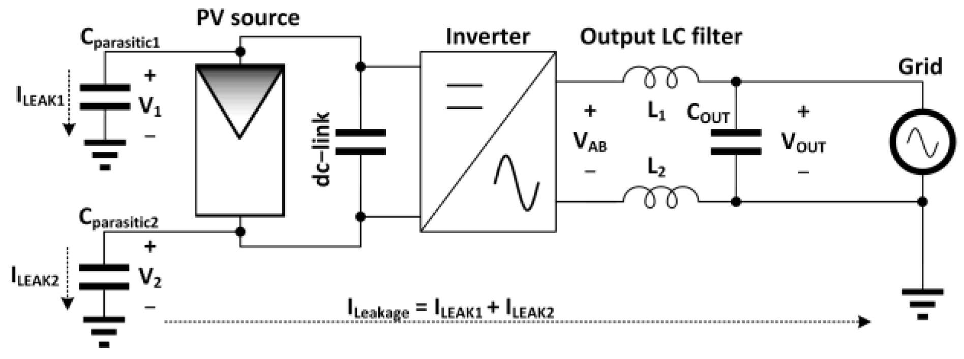
:1. Introduction
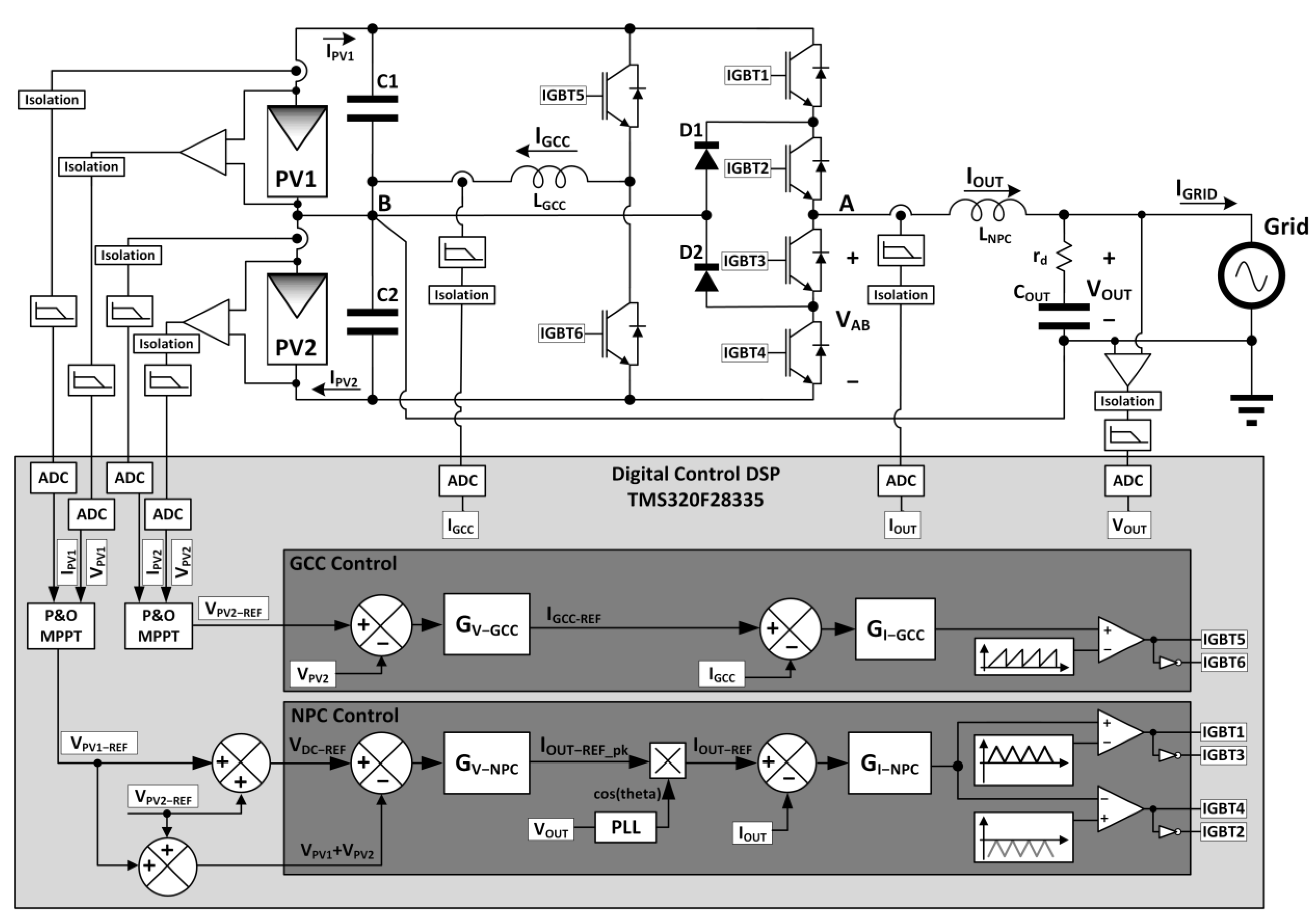
2. Transformerless PV Inverter Control Structure
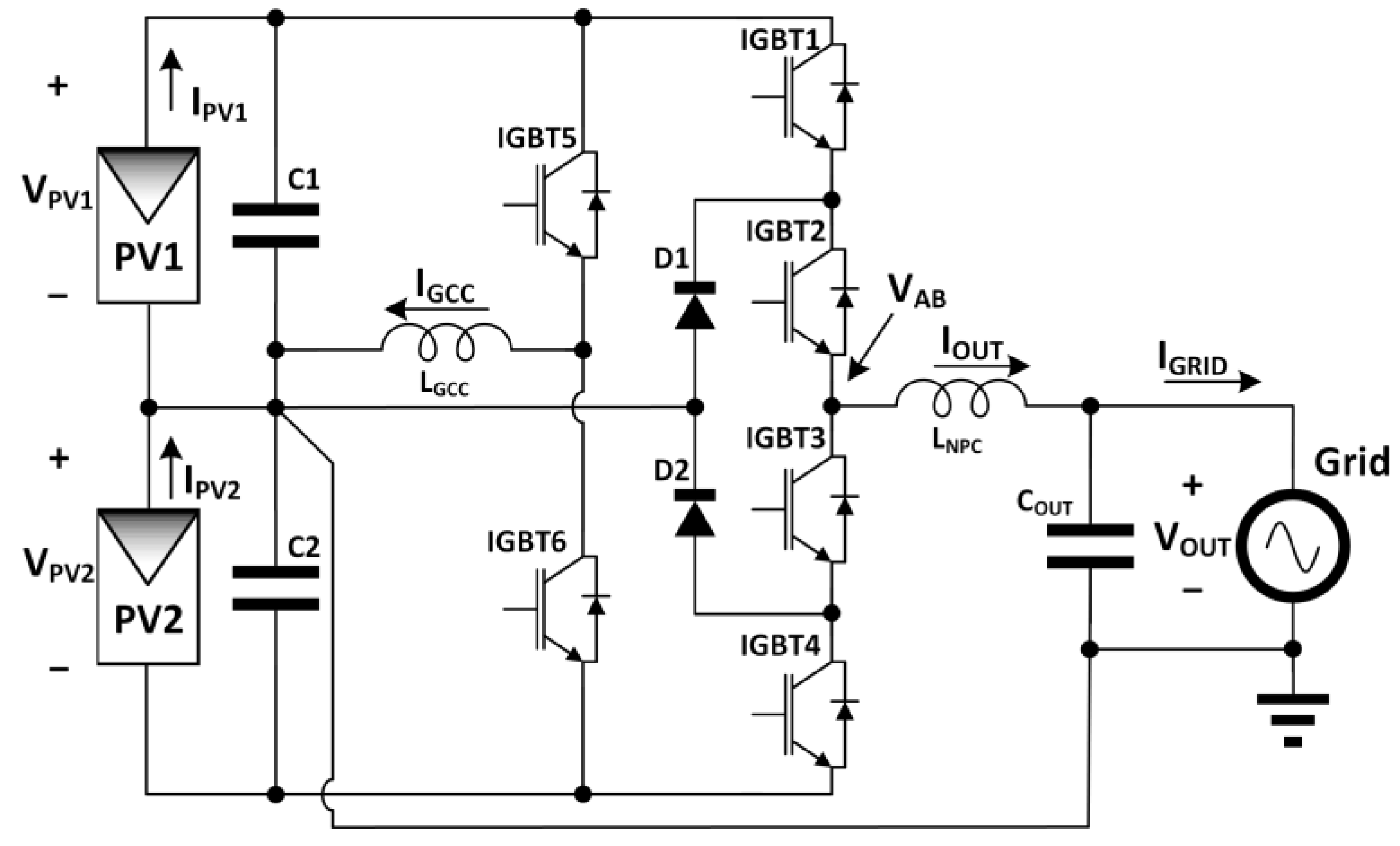
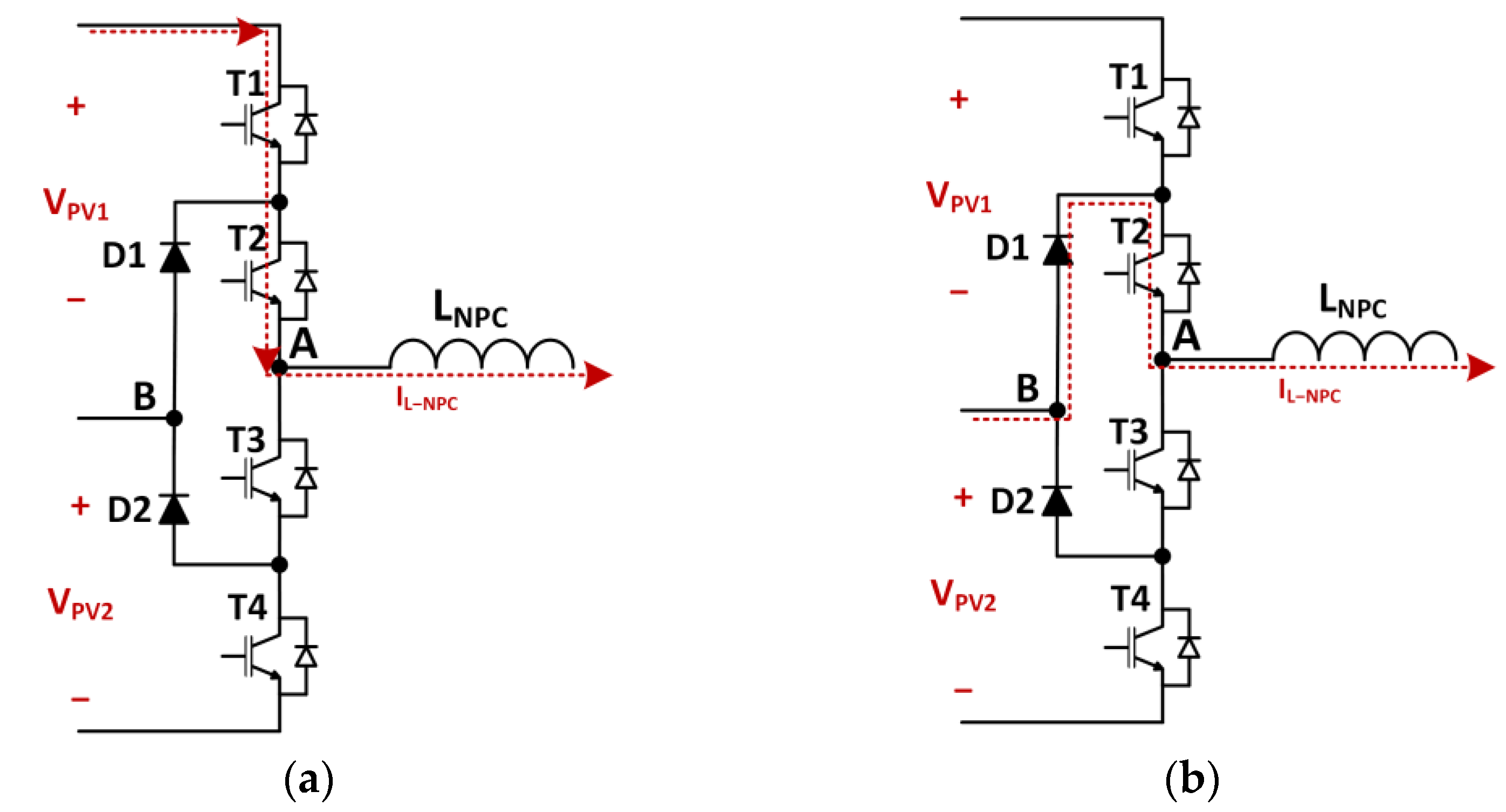
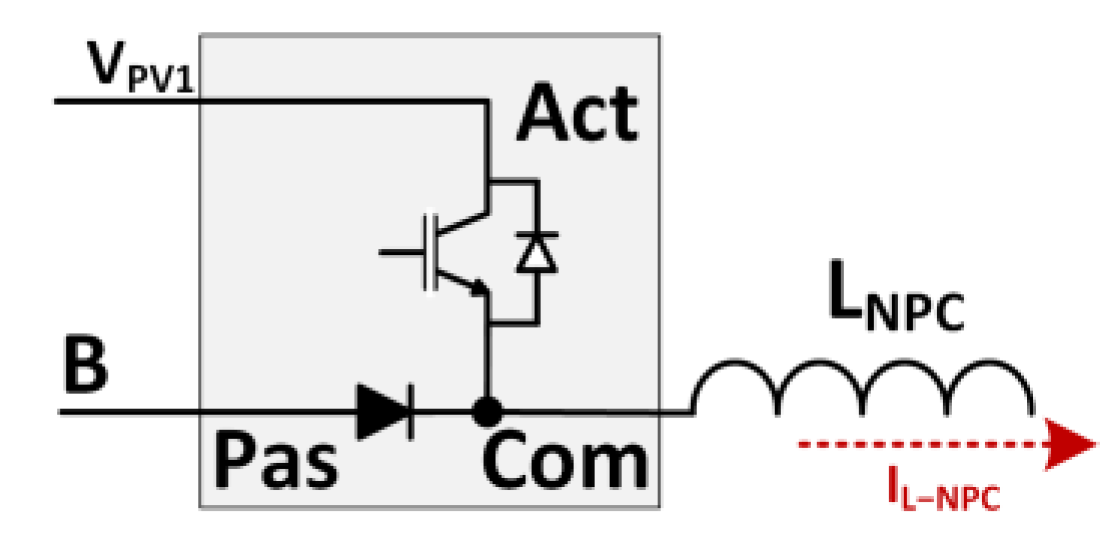
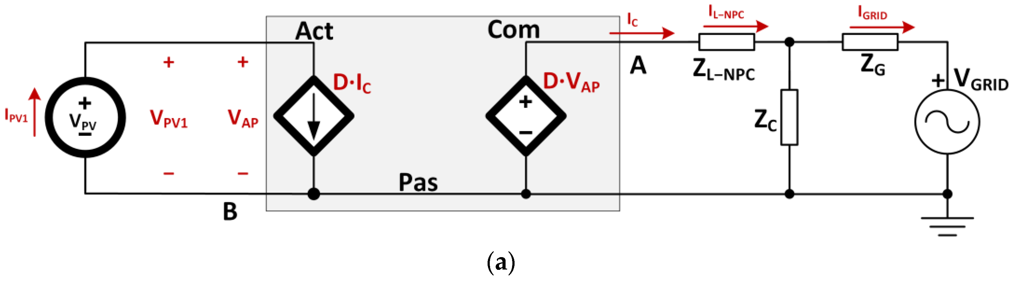
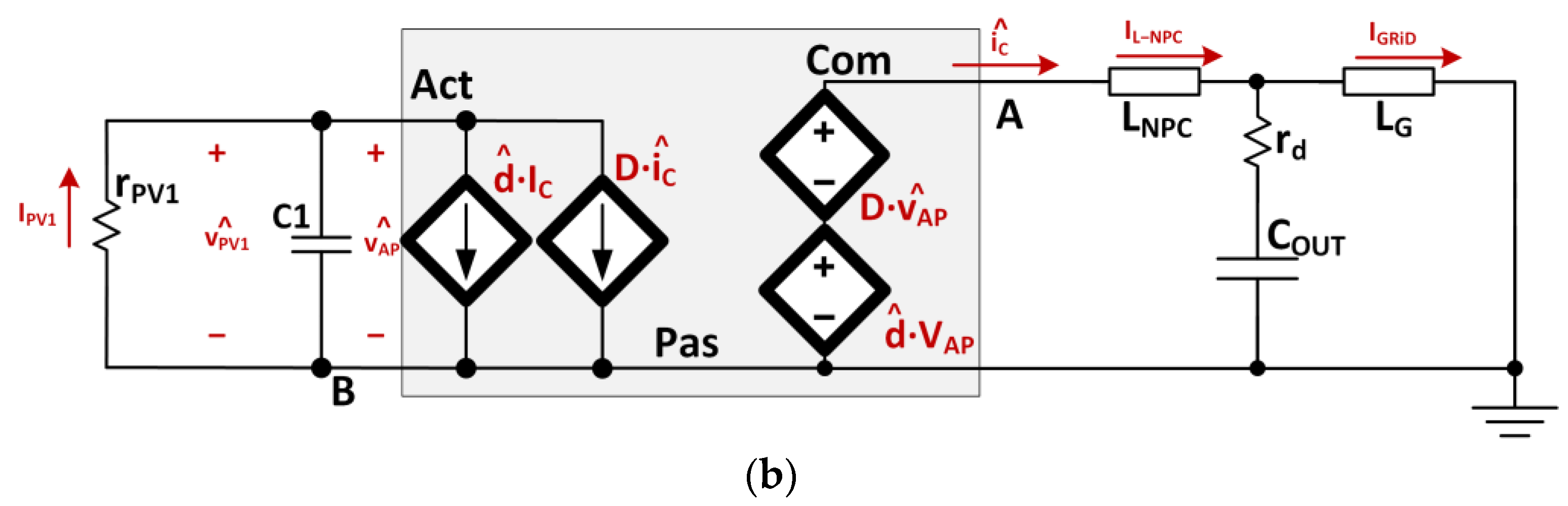
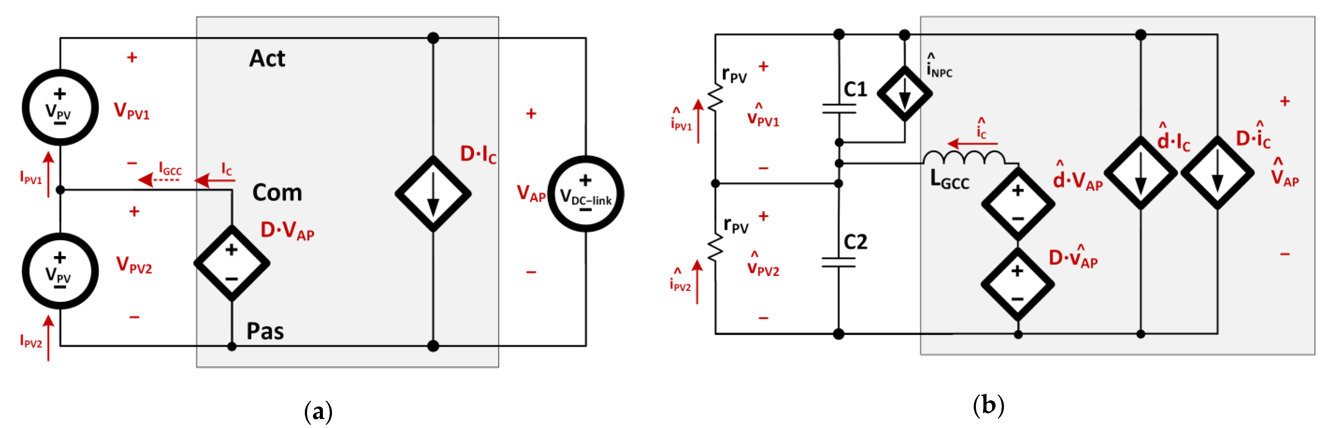
2.1. Model and Control Structure of the Multilevel Half-Bridge NPC PWM Inverter
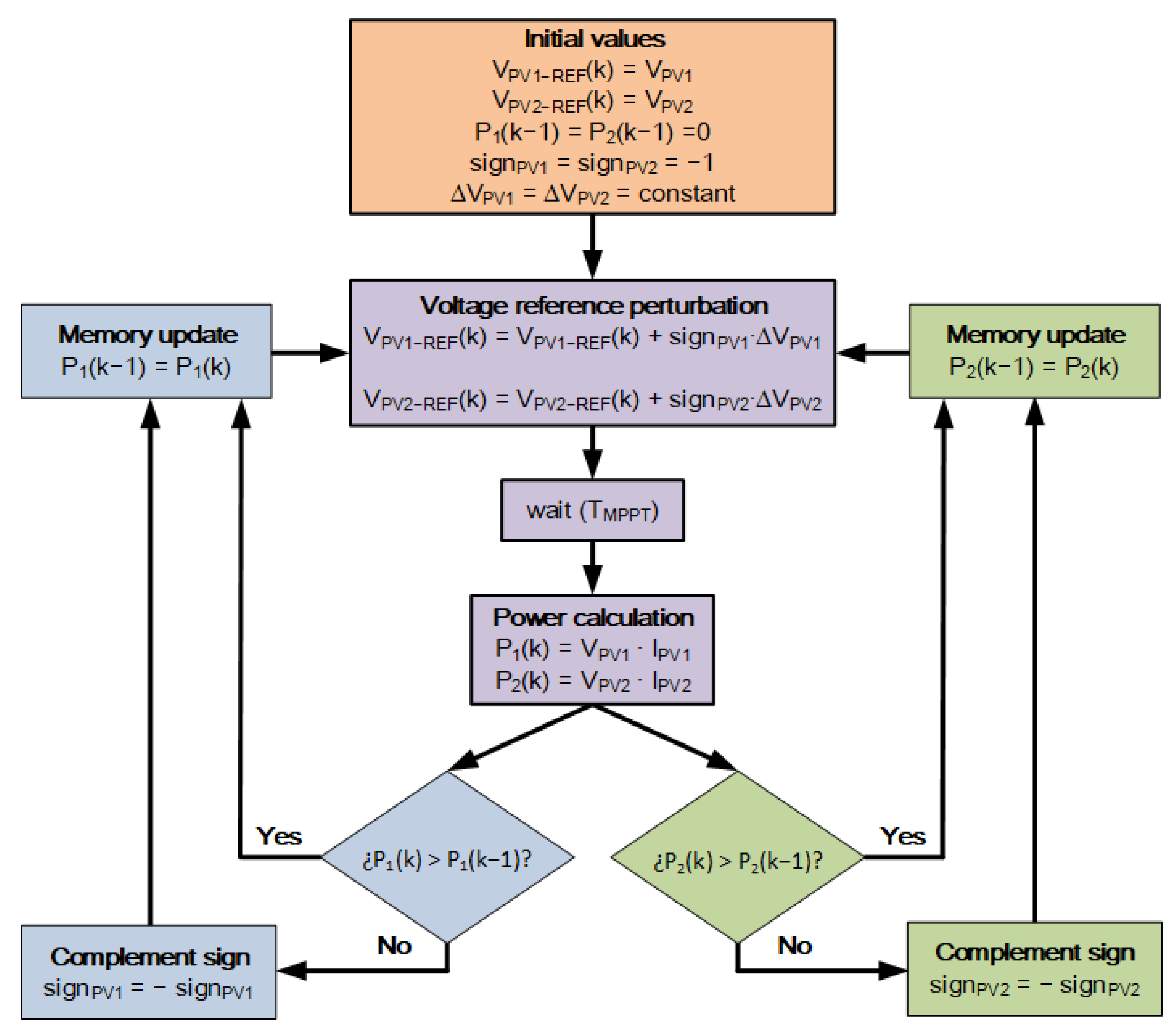
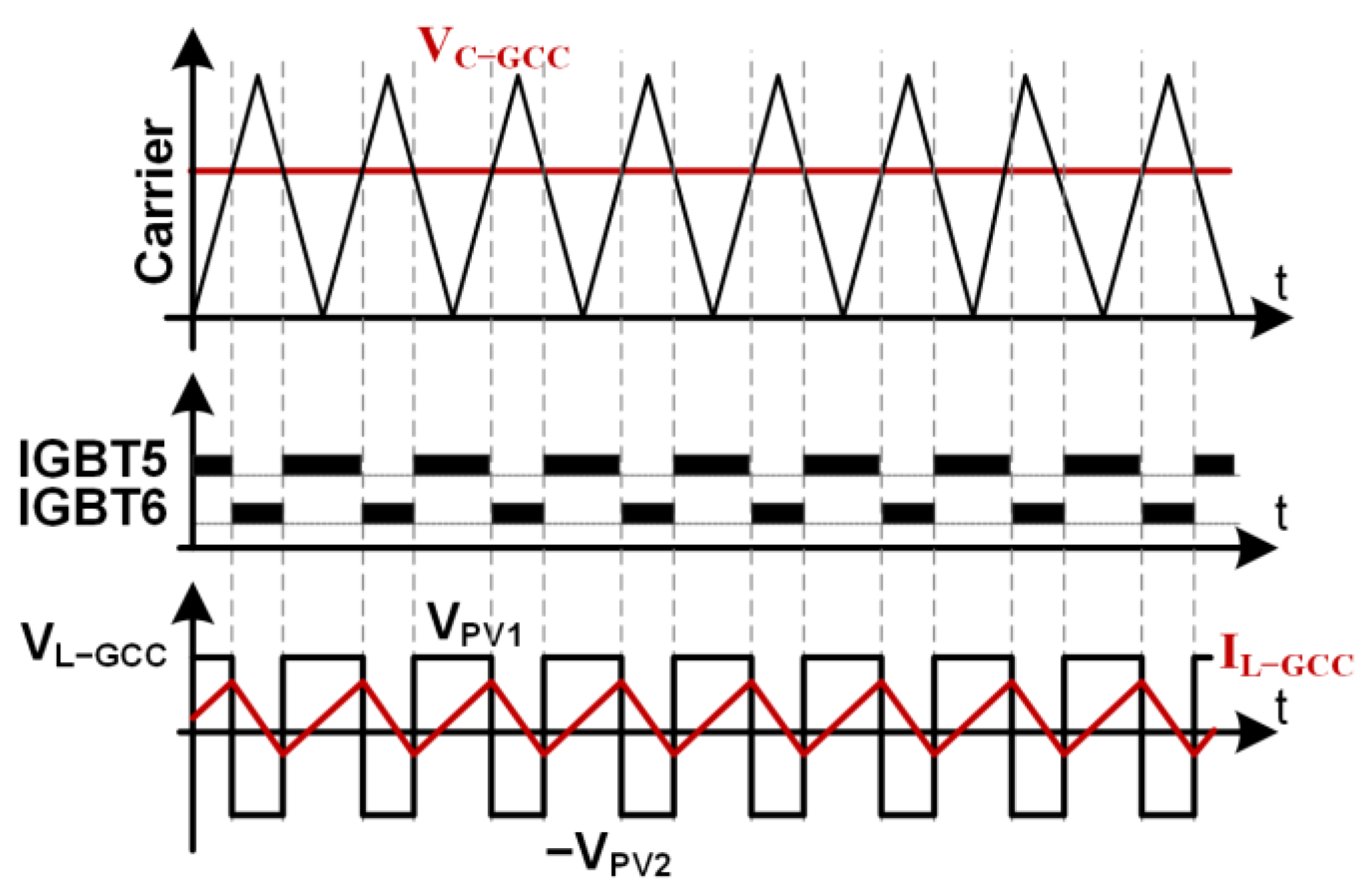
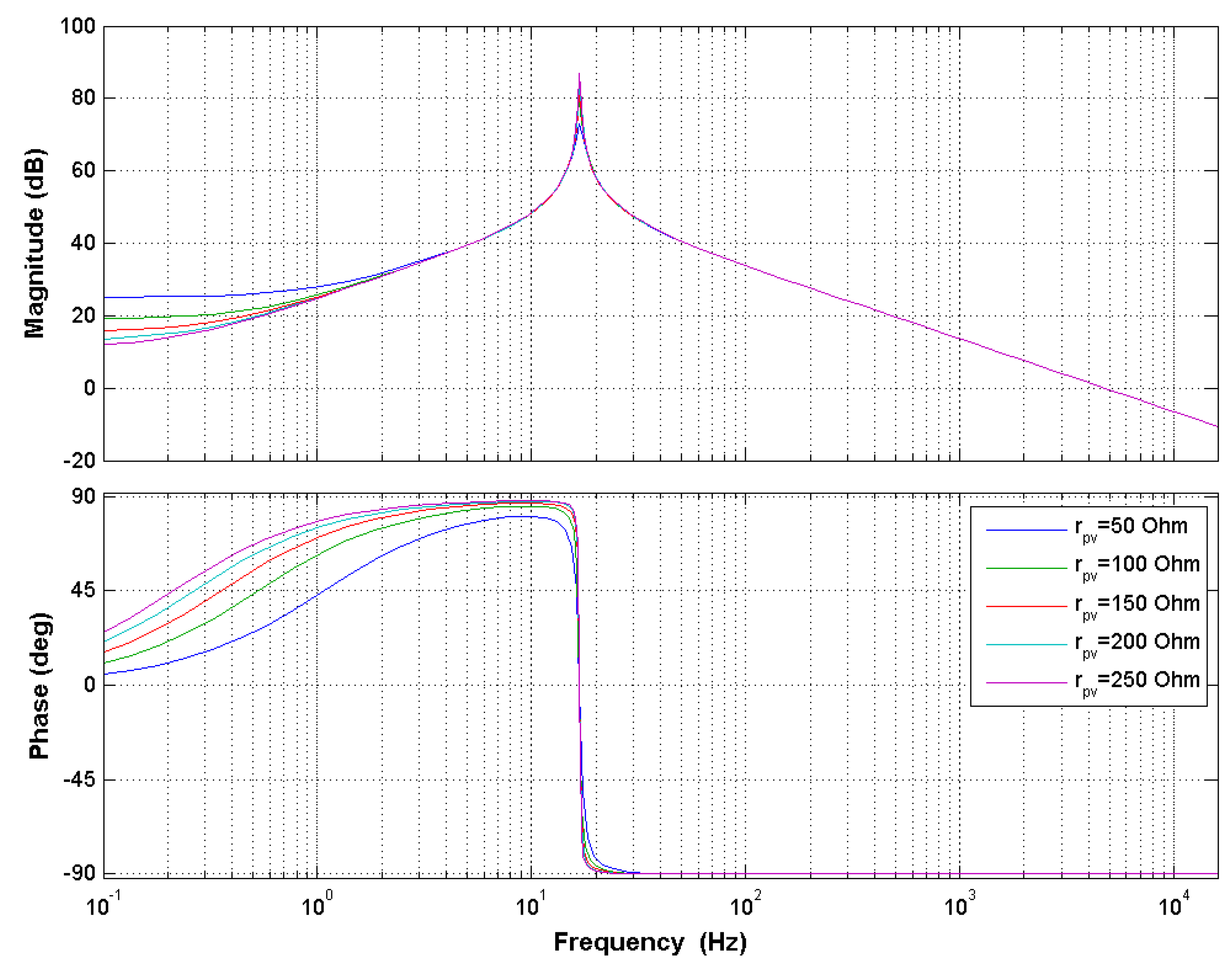
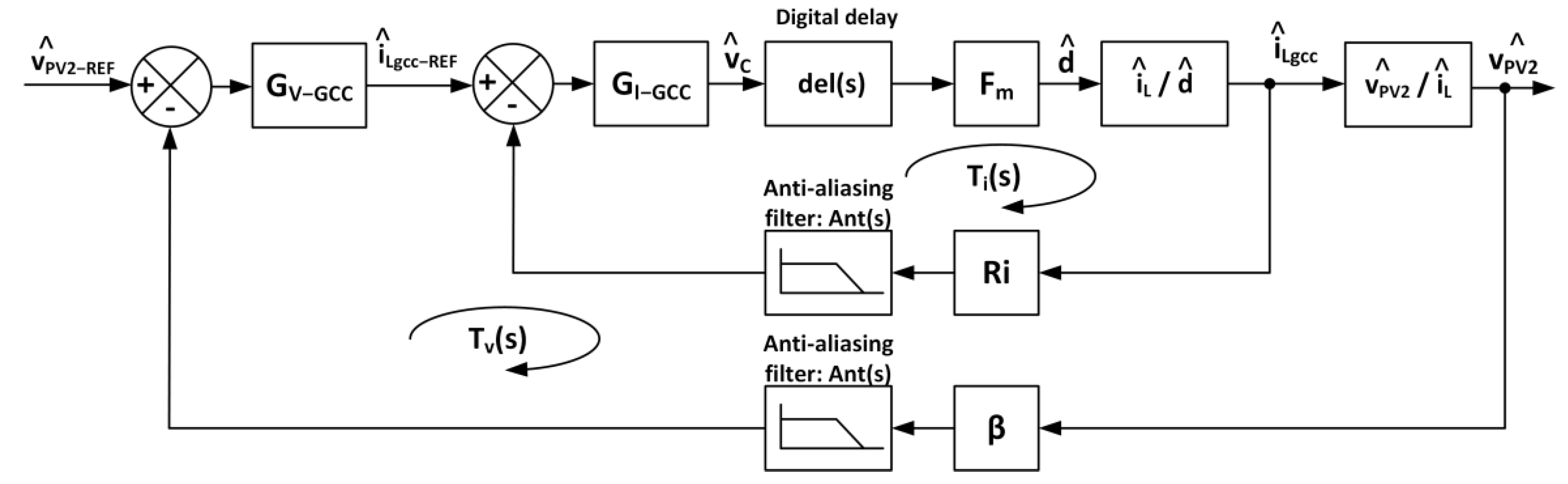
2.2. Model and Control Structure of the GCC DC/DC Converter
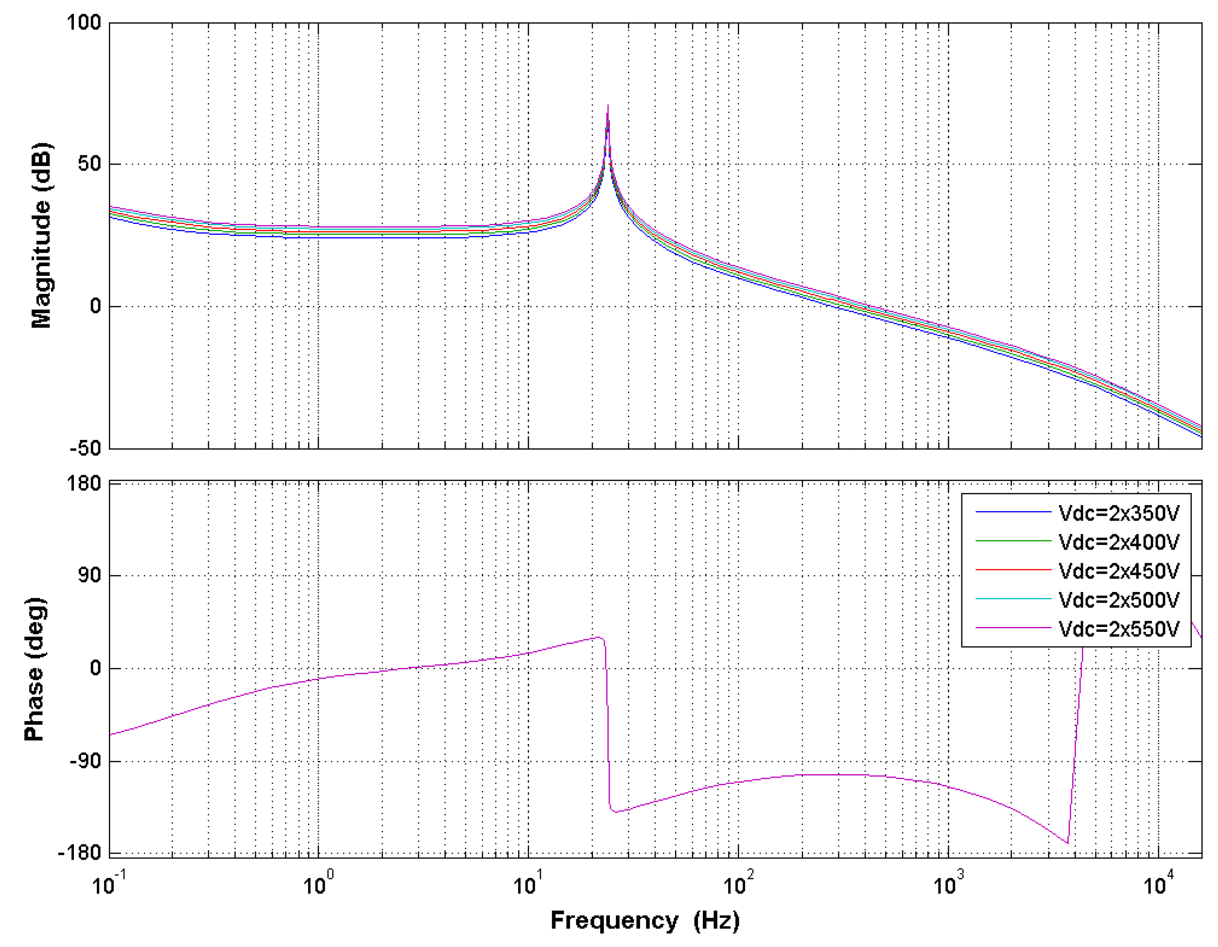
3. Control Design of NPC PWM Inverter
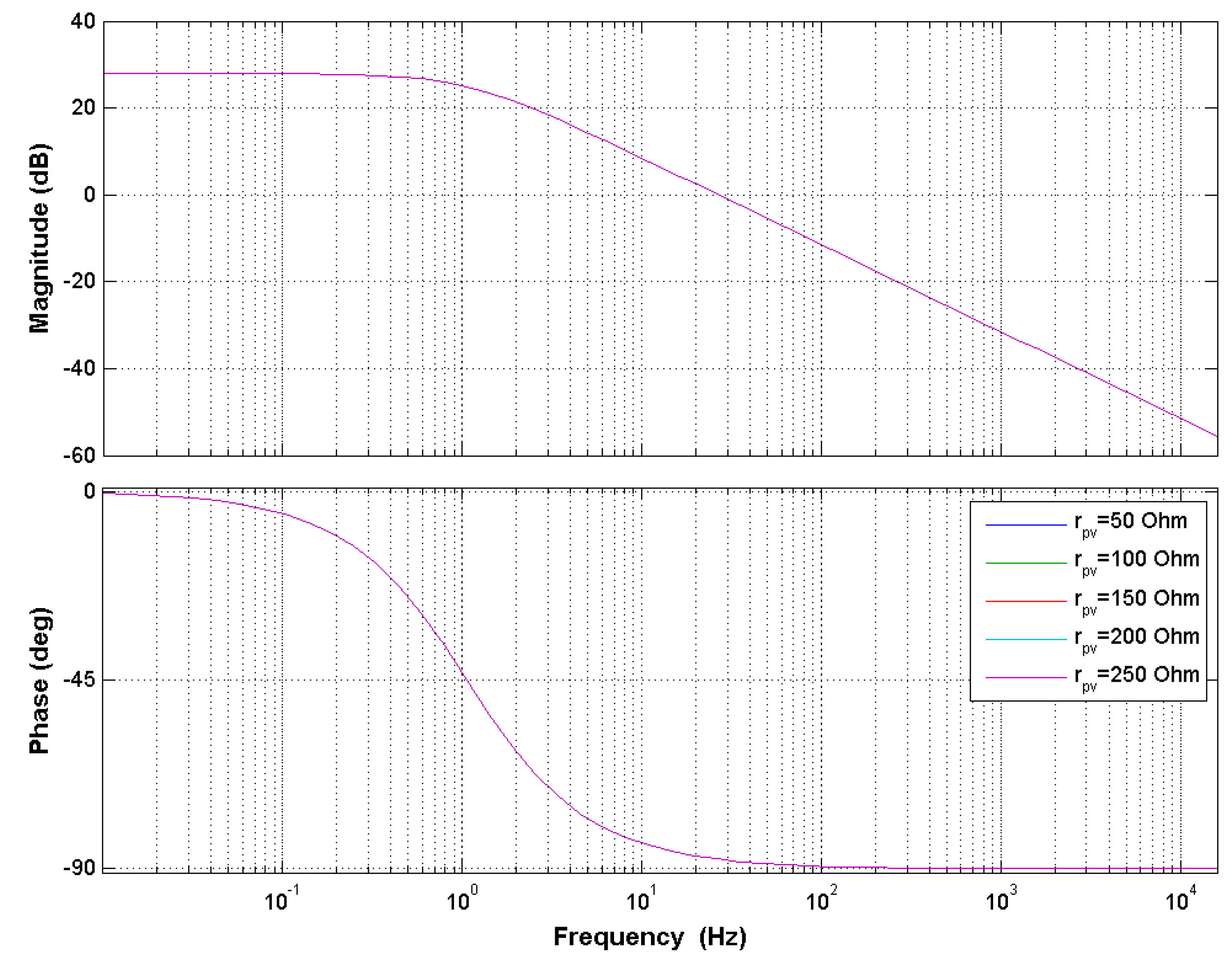
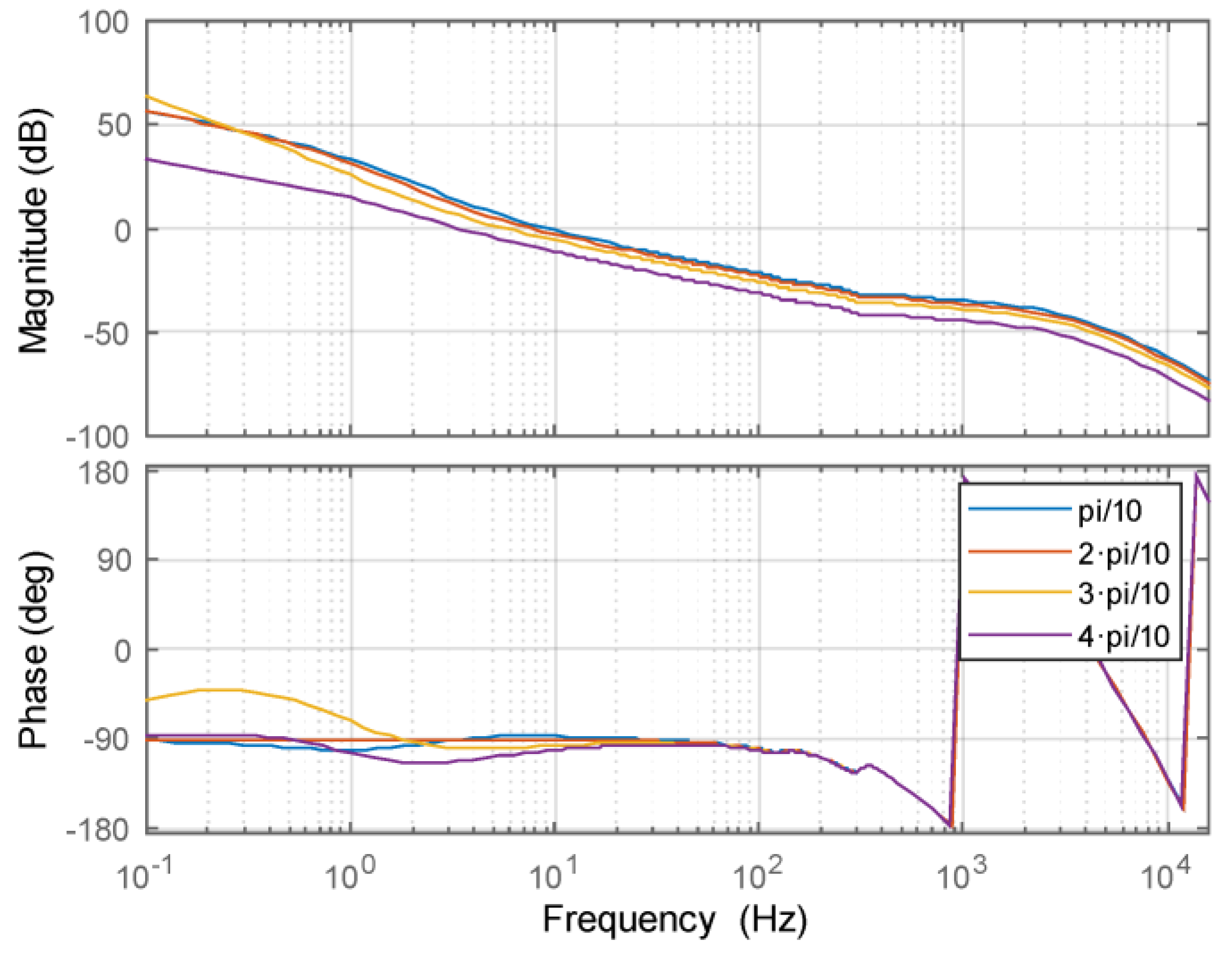
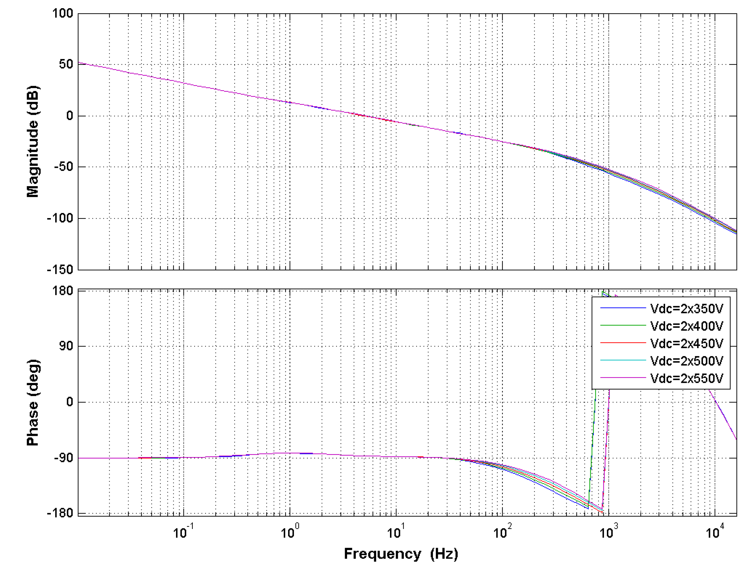
4. Control Design of GCC DC/DC Converter
5. Conclusions
Author Contributions
Funding
Data Availability Statement
Conflicts of Interest
References
- Patrao, I.; Figueres, E.; González-Espín, F.; Garcerá, G. Transformerless topologies for grid-connected single-phase photovoltaic inverters. Renew. Sustain. Energy Rev. 2011, 15, 3423–3431. [Google Scholar] [CrossRef]
- Liberos, M.; González-Medina, R.; Garcerá, G.; Figueres, E. A Method to Enhance the Global Efficiency of High-Power Photovoltaic Inverters Connected in Parallel. Energies 2019, 12, 2219. [Google Scholar] [CrossRef]
- Vo, D.-V.; Nguyen, K.M.; Lim, Y.-C.; Choi, J.-H. A Single-Stage Bimodal Transformerless Inverter with Common-Ground and Buck-Boost Features. Electronics 2023, 12, 221. [Google Scholar] [CrossRef]
- Amoiralis, E.I.; Tsili, M.A.; Kladas, A.G. Power Transformer Economic Evaluation in Decentralized Electricity Markets. IEEE Trans. Ind. Electron. 2011, 59, 2329–2341. [Google Scholar] [CrossRef]
- Kefalas, T.D.; Kladas, A.G. Analysis of Transformers Working Under Heavily Saturated Conditions in Grid-Connected Renewable-Energy Systems. IEEE Trans. Ind. Electron. 2011, 59, 2342–2350. [Google Scholar] [CrossRef]
- Araujo, S.; Zacharias, P.; Sahan, B. Novel grid-connected non-isolated converters for photovoltaic systems with grounded generator. In Proceedings of the 2008 IEEE Power Electronics Specialists Conference, Rhodes, Greece, 15–19 June 2008; pp. 58–65. [Google Scholar] [CrossRef]
- Li, W.; Gu, Y.; Luo, H.; Cui, W.; He, X.; Xia, C. Topology Review and Derivation Methodology of Single-Phase Transformerless Photovoltaic Inverters for Leakage Current Suppression. IEEE Trans. Ind. Electron. 2015, 62, 4537–4551. [Google Scholar] [CrossRef]
- Wang, L.; Chen, L.; Ye, W.; Ma, W. Phase-Shifted Energy Balance Control for Multilevel Inverters in Grid-Connected PV Systems. Electronics 2023, 12, 2582. [Google Scholar] [CrossRef]
- Chen, B.; Gu, B.; Zhang, L.; Zahid, Z.U.; Lai, J.-S.; Liao, Z.; Hao, R. A High-Efficiency MOSFET Transformerless Inverter for Nonisolated Microinverter Applications. IEEE Trans. Power Electron. 2014, 30, 3610–3622. [Google Scholar] [CrossRef]
- Kerekes, T.; Teodorescu, R.; Rodriguez, P.; Vazquez, G.; Aldabas, E. A New High-Efficiency Single-Phase Transformerless PV Inverter Topology. IEEE Trans. Ind. Electron. 2009, 58, 184–191. [Google Scholar] [CrossRef]
- Salas, V.; Olías, E. Overview of the state of technique for PV inverters used in low voltage grid-connected PV systems: Inverters below 10kW. Renew. Sustain. Energy Rev. 2009, 13, 1541–1550. [Google Scholar] [CrossRef]
- Xiao, H.F.; Lan, K.; Zhang, L. A Quasi-Unipolar SPWM Full-Bridge Transformerless PV Grid-Connected Inverter with Constant Common-Mode Voltage. IEEE Trans. Power Electron. 2014, 30, 3122–3132. [Google Scholar] [CrossRef]
- López, Ó.; Freijedo, F.D.; Yepes, A.G.; Fernández-Comesaña, P.; Malvar, J.; Teodorescu, R.; Doval-Gandoy, J. Eliminating Ground Current in a Transformerless Photovoltaic Application. IEEE Trans. Energy Convers. 2010, 25, 140–147. [Google Scholar] [CrossRef]
- Gonzalez, R.; Gubia, E.; Lopez, J.; Marroyo, L. Transformerless Single-Phase Multilevel-Based Photovoltaic Inverter. IEEE Trans. Ind. Electron. 2008, 55, 2694–2702. [Google Scholar] [CrossRef]
- Tang, Y.; Yao, W.; Loh, P.C.; Blaabjerg, F. Highly Reliable Transformerless Photovoltaic Inverters with Leakage Current and Pulsating Power Elimination. IEEE Trans. Ind. Electron. 2015, 63, 1016–1026. [Google Scholar] [CrossRef]
- Vazquez, N.; Rosas, M.; Hernandez, C.; Vazquez, E.; Perez-Pinal, F.J. A New Common-Mode Transformerless Photovoltaic Inverter. IEEE Trans. Ind. Electron. 2015, 62, 6381–6391. [Google Scholar] [CrossRef]
- Zhou, L.; Gao, F. Low leakage current single-phase PV inverters with universal neutral-point-clamping method. In Proceedings of the 2016 IEEE Applied Power Electronics Conference and Exposition (APEC), Long Beach, CA, USA, 20–24 March 2016; pp. 410–416. [Google Scholar] [CrossRef]
- Patrao, I.; Garcerá, G.; Figueres, E.; González-Medina, R. Grid-tie inverter topology with maximum power extraction from two photovoltaic arrays. IET Renew. Power Gener. 2014, 8, 638–648. [Google Scholar] [CrossRef]
- Zhang, Q.; Sun, X.; Zhong, Y.; Matsui, M. A Novel Topology for Solving the Partial Shading Problem in Photovoltaic Power Generation System. In Proceedings of the 2009 IEEE 6th International Power Electronics and Motion Control Conference, Wuhan, China, 17–20 May 2009; pp. 2130–2135. [Google Scholar]
- Daher, S.; Schmid, J.; Antunes, F.L.M. Multilevel Inverter Topologies for Stand-Alone PV Systems. IEEE Trans. Ind. Electron. 2008, 55, 2703–2712. [Google Scholar] [CrossRef]
- Kjaer, S.; Pedersen, J.; Blaabjerg, F. A Review of Single-Phase Grid-Connected Inverters for Photovoltaic Modules. IEEE Trans. Ind. Appl. 2005, 41, 1292–1306. [Google Scholar] [CrossRef]
- Memon, R.; Mahar, M.A.; Larik, A.S.; Shah, S.A.A. Design and Performance Analysis of New Multilevel Inverter for PV System. Sustainability 2023, 15, 10629. [Google Scholar] [CrossRef]
- Debdouche, N.; Deffaf, B.; Benbouhenni, H.; Laid, Z.; Mosaad, M.I. Direct Power Control for Three-Level Multifunctional Voltage Source Inverter of PV Systems Using a Simplified Super-Twisting Algorithm. Energies 2023, 16, 4103. [Google Scholar] [CrossRef]
- Zaid, S.A.; Bakeer, A.; Albalawi, H.; Alatwi, A.M.; Abdeldaim, H.; Manqarah, B. Model-Free Predictive Current Control of a 3-φ Grid-Connected Neutral-Point-Clamped Transformerless Inverter. Energies 2023, 16, 3141. [Google Scholar] [CrossRef]
- Alghamdi, T.A.; Anayi, F.; Packianather, M. Modelling and Control Development of a Cascaded NPC-Based MVDC Converter for Harmonic Analysis Studies in Power Distribution Network. Energies 2022, 15, 4867. [Google Scholar] [CrossRef]
- Serban, E.; Ordonez, M.; Pondiche, C.; Hulea, D. Voltage and Power Balancing in Solar and Energy Storage Converters. In Proceedings of the 2019 IEEE Energy Conversion Congress and Exposition (ECCE), Baltimore, MD, USA, 29 September–3 October 2019; pp. 5832–5839. [Google Scholar] [CrossRef]
- Ji, Y.-H.; Jung, D.-Y.; Kim, J.-G.; Kim, J.-H.; Lee, T.-W.; Won, C.-Y. A Real Maximum Power Point Tracking Method for Mismatching Compensation in PV Array Under Partially Shaded Conditions. IEEE Trans. Power Electron. 2010, 26, 1001–1009. [Google Scholar] [CrossRef]
- De Brito, M.A.G.; Galotto, L.; Sampaio, L.P.; Melo, G.D.A.E.; Canesin, C.A. Evaluation of the Main MPPT Techniques for Photovoltaic Applications. IEEE Trans. Ind. Electron. 2013, 60, 1156–1167. [Google Scholar] [CrossRef]
- Lim, Z.; Tafti, H.D.; Pinkymol, H.R. Multilevel Modulation Methods. In Advanced Multilevel Converters and Applications in Grid Integration; Maswood, A.I., Tafti, H.D., Eds.; John Wiley & Sons: Chichester, UK, 2018. [Google Scholar] [CrossRef]
- Ram, J.P.; Babu, T.S.; Rajasekar, N. A comprehensive review on solar PV maximum power point tracking techniques. Renew. Sustain. Energy Rev. 2017, 67, 826–847. [Google Scholar] [CrossRef]
- Mastromauro, R.A.; Liserre, M.; Dell'Aquila, A. Control Issues in Single-Stage Photovoltaic Systems: MPPT, Current and Voltage Control. IEEE Trans. Ind. Inform. 2012, 8, 241–254. [Google Scholar] [CrossRef]
- Golestan, S.; Monfared, M.; Freijedo, F.D. Design-Oriented Study of Advanced Synchronous Reference Frame Phase-Locked Loops. IEEE Trans. Power Electron. 2012, 28, 765–778. [Google Scholar] [CrossRef]
- Gazoli, J.R.; Villalva, M.G.; Siqueira, T.G.; Ruppert, E. Micro-Inverter for Integrated Grid-Tie PV Module Using Resonant Controller. In Proceedings of the 2012 IEEE Power and Energy Society General Meeting, San Diego, CA, USA, 22–26 July 2012; pp. 1–8. [Google Scholar]
- Lan, Z.; Li, Y.; Li, C.; Zhu, C.; Wang, C. Investigation on IGCT-Based NPC/H-Bridge Large Power Converter. In Proceedings of the 2012 IEEE Energy Conversion Congress and Exposition (ECCE), Raleigh, NC, USA, 15–20 September 2012; pp. 726–730. [Google Scholar]
- Feng, T.; Chen, C.; Li, J.; Zhang, H.; Wang, K. Research on the modeling method of NPC three-phase three-level inverter. In Proceedings of the 2020 Chinese Automation Congress (CAC), Shanghai, China, 6–8 November 2020; pp. 3808–3813. [Google Scholar] [CrossRef]
- Kong, D.; Zhang, Z.; Liu, C.; Tian, W.; Gao, X.; Kennel, R. Modulated Model Predictive Control of Power Electronics Transformer Based on Isolated Modular Multilevel Converter. In Proceedings of the 2021 IEEE International Conference on Predictive Control of Electrical Drives and Power Electronics (PRECEDE), Jinan, China, 20–22 November 2021; pp. 831–835. [Google Scholar] [CrossRef]
- Yoon, H.; Cho, Y. Modulated Model Predictive Current Control for Three-Phase NPC Inverter with an LC Filter. In Proceedings of the 2022 5th International Conference on Power Engineering and Renewable Energy (ICPERE), Bandung, Indonesia, 22–23 November 2022; Volume 1, pp. 1–5. [Google Scholar] [CrossRef]
- Boumaaraf, H.; Talha, A.; Bouhali, O. A three-phase NPC grid-connected inverter for photovoltaic applications using neural network MPPT. Renew. Sustain. Energy Rev. 2015, 49, 1171–1179. [Google Scholar] [CrossRef]
- Rasoanarivo, I.; Arab-Tehrani, K.; Sargos, F.-M. Fractional Order PID and Modulated Hysteresis for high performance current control in multilevel inverters. In Proceedings of the 2011 IEEE Industry Applications Society Annual Meeting, Orlando, FL, USA, 9–13 October 2011; pp. 1–7. [Google Scholar] [CrossRef]
- Pimentel, S.P.; Husev, O.; Stepenko, S.; Vinnikov, D.; Roncero-Clemente, C.; Makovenko, E. Voltage Control Tuning of a Single-Phase Grid-Connected 3L qZS-Based Inverter for PV Application. In Proceedings of the 2018 IEEE 38th International Conference on Electronics and Nanotechnology (ELNANO), Kyiv, Ukraine, 24–26 April 2018; pp. 692–698. [Google Scholar] [CrossRef]
- Vorperian, V. Simplified analysis of PWM converters using model of PWM switch. Continuous conduction mode. IEEE Trans. Aerosp. Electron. Syst. 1990, 26, 490–496. [Google Scholar] [CrossRef]
- Shimizu, T.; Hirakata, M.; Kamezawa, T.; Watanabe, H. Generation control circuit for photovoltaic modules. IEEE Trans. Power Electron. 2001, 16, 293–300. [Google Scholar] [CrossRef]


| Parameter | Value |
|---|---|
| Input voltage at MPP (VPV-MPP) | 2 × 408.8 V |
| Input current at MPP (IMPP) | 7.54 ADC |
| Maximum PV power (PPV-MAX) | 2 × 3.08 kW |
| GCC switching frequency (fSW-GCC) | 16 kHz |
| NPC switching frequency (fSW-NPC) | 16 kHz |
| Input capacitance (C1 and C2) | 2 × 3 mF |
| GCC inductance (LGCC) | 15 mH |
| NPC inductance (LNPC) | 2 mH |
| LC filter capacitance (COUT) | 9.4 µF |
| Damping resistor (rd) | 1 Ω |
| GCC IGBT switches | IRG4PH40KDPBF (1200 V/15 A) |
| NPC IGBT switches | APTGL60TL120T3G (1200 V/60 A) |
| RMS nominal grid voltage (VGRID-RMS) | 230 VRMS |
| Nominal grid frequency (fGRID) | 50 Hz |
| Anti-aliasing filters crossover frequency | 16 kHz |
| ADC sampling frequency | 32 kHz |
| Digital voltage regulators update frequency | 32 kHz |
| Digital current regulators update frequency | 32 kHz |
| MPPT update period | 300 ms |
| Name | Value/Expression |
|---|---|
| Digital delay of one sampling period (TS = 31.25 µs), del(s) | |
| Modulator gain, Fm | 1 |
| Current sensor gain, Ri | 1 |
| Voltage sensor gain, β | 1 |
| Current regulator, GI-NPC(s) | |
| Closed loop response of the output current to its reference | |
| Voltage regulator, GV-NPC(s) | |
| Loop gain of the voltage loop, TV(s) | |
| Closed loop response of the output current to its reference |
| Name | Value/Expression |
|---|---|
| Digital delay of one sampling period (TS = 31.25 µs), del(s) | |
| Modulator gain, Fm | 1 |
| Current sensor gain, Ri | 1 |
| Voltage sensor gain, β | 1 |
| Current regulator, GI-GCC(s) | |
| Loop gain of the current loop, Ti(s) | |
| Closed loop response of the output current to its reference | |
| Voltage regulator, GV-GCC(s) | |
| Loop gain of the voltage loop, TV(s) | |
| Closed loop response of the output current to its reference |
Disclaimer/Publisher’s Note: The statements, opinions and data contained in all publications are solely those of the individual author(s) and contributor(s) and not of MDPI and/or the editor(s). MDPI and/or the editor(s) disclaim responsibility for any injury to people or property resulting from any ideas, methods, instructions or products referred to in the content. |
© 2023 by the authors. Licensee MDPI, Basel, Switzerland. This article is an open access article distributed under the terms and conditions of the Creative Commons Attribution (CC BY) license (https://creativecommons.org/licenses/by/4.0/).
Share and Cite
Patrao, I.; Liberos, M.; González-Medina, R.; Torán, E.; Figueres, E.; Garcerá, G. Small-Signal Model of the NPC + GCC Multilevel Transformerless Inverter in Single-Phase Photovoltaic Power Systems. Electronics 2023, 12, 3545. https://doi.org/10.3390/electronics12173545
Patrao I, Liberos M, González-Medina R, Torán E, Figueres E, Garcerá G. Small-Signal Model of the NPC + GCC Multilevel Transformerless Inverter in Single-Phase Photovoltaic Power Systems. Electronics. 2023; 12(17):3545. https://doi.org/10.3390/electronics12173545
Chicago/Turabian StylePatrao, Iván, Marian Liberos, Raúl González-Medina, Enric Torán, Emilio Figueres, and Gabriel Garcerá. 2023. "Small-Signal Model of the NPC + GCC Multilevel Transformerless Inverter in Single-Phase Photovoltaic Power Systems" Electronics 12, no. 17: 3545. https://doi.org/10.3390/electronics12173545
APA StylePatrao, I., Liberos, M., González-Medina, R., Torán, E., Figueres, E., & Garcerá, G. (2023). Small-Signal Model of the NPC + GCC Multilevel Transformerless Inverter in Single-Phase Photovoltaic Power Systems. Electronics, 12(17), 3545. https://doi.org/10.3390/electronics12173545