Abstract
This paper presents a throughput/area-efficient hardware accelerator architecture for elliptic curve point multiplication (ECPM) computation over . The throughput of the proposed accelerator design is optimized by reducing the total clock cycles using a bit-parallel Karatsuba modular multiplier. We employ two techniques to minimize the hardware resources: (i) a consolidated arithmetic unit where we combine a single modular adder, multiplier, and square block instead of having multiple modular operators, and (ii) an Itoh–Tsujii inversion algorithm by leveraging the existing hardware resources of the multiplier and square units for multiplicative inverse computation. An efficient finite-state-machine (FSM) controller is implemented to facilitate control functionalities. To evaluate and compare the results of the proposed accelerator architecture against state-of-the-art solutions, a figure-of-merit (FoM) metric in terms of throughput/area is defined. The implementation results after post-place-and-route simulation are reported for reconfigurable field-programmable gate array (FPGA) devices. Particular to Virtex-7 FPGA, the accelerator utilizes 3584 slices, needs 7208 clock cycles, operates on a maximum frequency of 350 MHz, computes one ECPM operation in 20.59 s, and the calculated value of FoM is 13.54. Consequently, the results and comparisons reveal that our accelerator suits applications that demand throughput and area-optimized ECPM implementations.
1. Introduction
The rapid increase in applications related to information technology has dramatically influenced the economy and culture in recent years [1]. This rapid increase has opened several security doors, leading to new critical threats for the community. Amongst several others, cryptography is one technique that offers secure information sharing on many electronic devices [2,3]. Therefore, two types of cryptographic algorithms exist: (i) symmetric key and (ii) asymmetric key. Symmetric key cryptographic algorithms utilize a single key for encryption and decryption. They are prevalent because of their high speed and ease of use. However, they require the two parties to agree on a secret key beforehand, which can be challenging. On the other hand, asymmetric cryptographic algorithms utilize two different keys, i.e., a private key and a public key. The public key is widely known and used to encrypt the original message. Similarly, the encrypted message can only be converted into the original message when the user has the corresponding private key. Consequently, asymmetric algorithms are more beneficial for long-term security and are the area of interest in this study.
Rivest–Shamir–Adleman (RSA) [4] and elliptic curve cryptography (ECC) [5] are the most well-known methods in asymmetric cryptography. Comparatively, the ECC requires shorter key lengths for equivalent security levels. Moreover, due to sits horter key sizes, the additional benefits of ECC are its lower channel bandwidth, computation time, and power consumption. Thus, this study utilized an ECC-based cryptoprocessor for cryptographic applications. It is essential to mention that the security of ECC relies on the discrete logarithm problem (DLP). It involves a model that comprises four layers for implementation [3,6]. The uppermost layer is the protocol layer that defines the rules for encryption and decryption, signature generation and verification for key authentication, and public key exchange. The essential operation in ECC is the elliptic curve point multiplication (ECPM) performed in the third layer. It depends on the point addition (PA) and double (PD) operations [3] performed in the second layer. Finally, modular arithmetic operations such as addition, multiplication, square, and inversion are required to perform these PA and PD computations.
In short, various settings are available to implement the (four) layer model of ECC. It includes the selection between two different basis representations (polynomial and normal) to represent the initial and final points. Furthermore, the choice between two coordinate systems (affine and projective) is critical [3]. We preferred a polynomial basis in this study, as it allows faster modular multiplications. On the other hand, a normal basis is helpful when frequent squares need to be implemented [6]. Additionally, we have selected a projective coordinate system as it concerns fewer inversion operations. Moreover, ECC offers prime and binary fields for implementation. The prime fields are denoted by with and 521. Similarly, the binary fields are specified by with and 571. Comparatively, the prime fields are suitable for software implementations, while the binary fields are more practical for hardware accelerations. As we dealt with hardware implementations, we selected binary fields for our implementations.
In addition to several ECC settings, software and hardware are two implementation platforms [2]. Comparatively, software platforms such as microcontrollers are more beneficial for flexible implementations. However, they provide limited speed/throughput. On the other hand, hardware platforms such as field-programmable gate arrays (FPGAs) and application-specific integrated circuits (ASICs) offer higher throughput with little flexibility. There is always a trade-off when selecting an appropriate implementation platform [7,8,9]. Thus, this study aimed to accelerate the ECPM operation of ECC on a FPGA platform for applications with limited hardware resources and power consumption.
1.1. Related ECPM Hardware Accelerators and Limitations
The Weierstrass, binary Huff curves (BHCs), Hessian, and binary Edward curves (BECs) are various ECC models. Therefore, the most related state-of-the-art hardware accelerators are described in [6,10,11,12,13,14,15,16,17,18,19]. Reference [6] proposes a pipelined architecture to accelerate ECPM operation by reducing the critical path delay. Moreover, PA and PD instructions are scheduled to reduce the latency or computation time. The design achieves a higher throughput/area ratio. It outperforms existing implementations, with synthesis results showing up to 369, 357, and 337 MHz frequencies for key lengths of 163, 233, and 283 bits, respectively, on the Virtex-7 FPGA. The design of [10] considers parallelism and Karatsuba–Offman–Algorithm (KOA) to optimize area, resulting in a highly flexible and fast ECC coprocessor architecture. Using 28 nm process technology by Taiwan Semiconductor Manufacturing Company (TSMC), the design of [10] obtains a circuit frequency 2.3 GHz, and one ECPM operation requires 0.26 s for computation.
The residue number system (RNS)-based coprocessor is presented in [11], where an efficient design is obtained using a highly pipelined multimodulo arithmetic unit. The implementation results on an FPGA demonstrated its small size and comparable performance to existing ECPM architectures. Also, the architecture allows flexible computation of different key sizes without requiring design modifications. The design of [12] aims to optimize hardware utilization and reduce power consumption by introducing a hybrid finite field multiplier that combines Karatsuba and shift-and-add multiplication algorithms. The multiplier performs one finite field multiplication in clock cycles for m-bit key length. Implementation and testing using Xilinx Vivado (ML Edition - 2023) and ISE Design Suite 14.7 design software showed promising results, indicating the suitability of the ECC accelerator for low-power, resource-constrained embedded systems applications.
An ECPM processor was efficiently implemented [13] on an FPGA using a bottom-up approach with three interdependent layers. Initially, they implemented an efficient digit-serial versatile multiplier (DSVM) using the four-way overlap-free Karatsuba algorithm (OFKA) and a modified radix-n interleaved multiplication technique. Secondly, they used the Lopez–Dahab (LD) Montgomery PM algorithm to enhance signal control and avoid data dependency in the ECPM design. Finally, the ECPM architecture was prototyped on an FPGA, indicating the lowest area-delay product (ADP) compared with that of existing structures for large field sizes.
The design of [14] implements the throughput/area-efficient ECPM architecture on ab FPGA. It includes a segmented pipelined digit-serial multiplier to enhance speed while minimizing area. Implementations on Virtex-4, Virtex-5, and Virtex-7 FPGAs achieved throughput/slice figures of 19.65, 65.30, and 64.48. The design of [15] introduces an ECPM architecture for generic irreducible polynomials using the modified Montgomery ladder algorithm. Moreover, they optimized the finite field inversion operation through the modified Itoh–Tsujii algorithm, which reduces the computation time. The implementation results showed that their architecture achieves significant area–time efficiency improvements. Like [14], the design of [16] implements a throughput/area ECPM architecture by proposing a two-stage pipelined design that reduces computation time through PA and PD instructions rescheduling and efficient memory utilization. Also, they offered a design of a 41-bit polynomial multiplier for binary field polynomial multiplications. They reported the implementation results on FPGA and ASIC platforms for NIST-recommended binary elliptic curve fields.
The designs reported in [6,10,11,12,13,14,15,16] cover the Weierstrass ECC model over a field. A Weierstrass ECC model over with p was implemented in [17], and the implementation results were demonstrated on a Xilinx Virtex-7 FPGA. The two-stage and four-stage pipelined BHC models of ECC were implemented [18,19], and the implementation results were reported on different Xilinx FPGA devices.
We must emphasize here that information security applications heavily rely on key authentication and exchange operations. For example, key authentication is essential when making payments online or in shopping centers. Similarly, key exchange is necessary for secure network/client communications [20,21,22]. Therefore, an elliptic curve digital signature algorithm (ECDSA) [23] is generally employed for key authentications. Moreover, the elliptic curve Diffie–Hellman (ECDH) [24] protocol is famous for key exchange mechanisms. Implementing ECDSA and ECDH algorithms relies on ECC’s efficient computation of ECPM operation. Therefore, several ECPM hardware accelerator designs, including [6,10,11,12,13,14,15,16], are tailored for optimizing area and throughput at the same time. Nevertheless, these accelerators lack discussion on the power consumption of their circuits, which is critical for various constrained applications such as radio-frequency identification (RFID) networks [25], wireless sensor networks (WSNs), and the Internet of things [26,27].
To summarize, multiple approaches have been implemented for performance improvement, e.g., the use of numerous modular operations in the data path of the processor designs [10,28], pipelining in the data path or modular multipliers [18,19,29], instruction-level parallelism [30], etc. These optimization strategies have resulted in overheads in hardware resource utilization and are inappropriate for RFID and WSN applications. Even if several hardware accelerators (in the literature) are optimized for area and throughput design parameters, including [6,10,11,12,13,14,15,16,18,19,28,29,30], there is always a possibility for further improvements in hardware resources, computation time, and consumed power by utilizing different design-level strategies.
1.2. Our Objective and Contributions
This study aimed to implement a hardware accelerator that simultaneously considers throughput and area optimizations. To achieve our objective, the key contributions of this study are as follows:
- We developed a throughput/area-efficient hardware accelerator architecture over with for ECPM computation.
- The throughput of the proposed accelerator architecture was optimized by reducing the total clock cycles. The clock cycles were optimized by implementing a bit-parallel Karatsuba modular multiplier.
- To optimize the area, instead of multiple modular operators, we incorporated a single modular adder, multiplier, and square block in the arithmetic unit of the proposed accelerator architecture. Moreover, we implemented an Itoh–Tsujii inversion algorithm [31] using the existing hardware resources of the Karatsuba multiplier and square units for the multiplicative inverse computations of ECC. These (two) strategies effectively minimized hardware resource utilization.
- A dedicated finite-state-machine (FSM) was implemented for control functionalities.
- A figure-of-merit (FoM) was defined in terms of throughput/area to provide a realistic comparison to state-of-the-art methods.
The remainder of this paper is structured as follows: Section 2 briefly overviews some of the most relevant literature. Section 3 describes the proposed architecture for the ECPM computation of ECC. The implementation results and comparison with state-of-the-art method are shown in Section 4. Finally, Section 5 provides the main findings of this study.
2. ECPM Algorithm over
The most critical ECPM operation of ECC is the computation of times the sum of an initial point P, as shown in Equation (1):
In Equation (1), P and Q represent the curve’s initial and resultant points, respectively, whereas d is a scalar multiplier or private key. Different algorithms for ECPM are available in the literature, including simple double and add, Montgomery .adder, and Lopez–Dahab, among others. A detailed comparison of different ECPM algorithms on FPGA and ASIC platforms can be found in [2]. Therefore, for our implementation, we opted for the Montgomery algorithm (Algorithm 1), which is inherently resistant to simple power analysis (SPA) attacks, which is a type of side channel attack to leak the secret during the power consumption of the circuit. It is important to emphasize that our focus was on SPA attacks at the algorithmic level, and we did not consider their realization on the design level.
The inputs to Algorithm 1 are the initial point P and a scalar multiplier d. A sequence determines the bits of the scalar multiplier in terms of zeros and ones. The output from Algorithm 1 is the x and y coordinates of resultant point Q. The PA and PD operations in Algorithm 1 show the number of instructions for point addition and double computations, respectively.
| Algorithm 1: Montgomery PM algorithm [6]. |
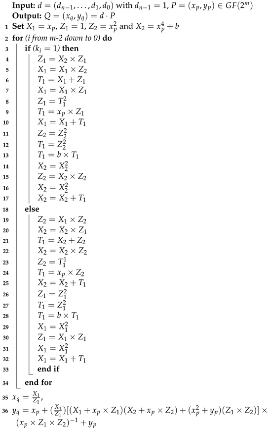 |
3. Proposed ECPM Hardware Architecture
The proposed ECPM accelerator architecture to implement Algorithm 1 is shown in Figure 1. It comprises a memory unit, a routing network, an arithmetic unit, and a control block. In addition to these critical blocks, the controller unit takes eight inputs and produces two outputs. The clk, rst, start, and din_ext are one-bit input signals. The key length is shown with m bits. x and y are the coordinates of initial point P (i.e., , and ). Similarly, con-b represents the curve constant. Moreover, done is a one-bit output signal while doutf is an m-bit output. The start signal specifies when the ECPM operation is needed to initiate the computation. The din_ext signal represents the inputs (such as xp, yp, key, and con-b). These inputs are needed to be loaded into the memory unit from outside. The done signal shows that the computation of the ECPM operation has finished. Finally, the doutf signal loads the generated output from the memory unit to the chip output. We provide the corresponding details of the various aforementioned units in the following sections.
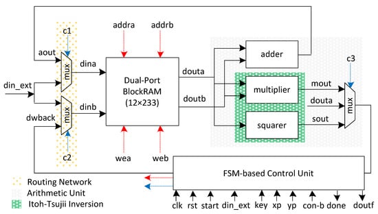
Figure 1.
Proposed hardware architecture for ECPM computation.
3.1. Memory Unit
A dual-port block RAM (DP-BRAM) of size was utilized, as shown in Figure 1. Here, 12 shows the number of addresses, and 233 indicates the number of bits stored on each memory address. It is important to mention that the BRAMs for FPGA designs offer a maximum 36-bit data width. Therefore, we generated an IP of a true DP-BRAM of , equivalent to six 36-bit data width BRAMs and one BRAM with an 18-bit data width. The total number of addresses was 12. Consequently, a 4-bit read/write address was needed to scan all addresses in the instantiated BRAM. The memory unit kept the initial point parameters ( and ) together with a curve constant (con-b). It also contained the intermediate results during Algorithm 1 and stored the resultant outputs. The reason for using dual-port memory is to read two operands for the arithmetic unit in one clock cycle. Furthermore, it also allows the writing o two results (where needed) after the computation in one clock cycle. The prefixes of the corresponding ports are ‘a’ and ‘b’. Similarly, ‘din’ and ‘dout’ represent the input and output data, respectively. The read/write addresses are shown with ‘addr’. A one-bit write-enable signal is used for read and write operations. The control unit generates the read/write addresses and the corresponding write-enable signal.
3.2. Routing Network
The orange dotted portion in Figure 1 shows the routing network, including two multiplexers. Each multiplexer contains an input of ‘din_ext’, which means the user wants to load external data on the utilized memory. The external data include the proposed ECPM processor architecture inputs and can be , , con-b, and key. Another input to the first multiplexer is from the output of the adder unit to write back the result of modular addition using an ‘aout’ signal, while the second input to the second multiplexer is from the multiplexed output of square and multiplier circuits, as shown in Figure 1. Using these two routing multiplexers in this way allows us to write two results in one clock cycle (if needed), resulting in a decrease in overall clock cycle counts. The blue dashed lines in Figure 1 are the control signals for the multiplexers, and generating these signals is the control unit’s responsibility.
3.3. Arithmetic Unit
The gray dotted area in Figure 1 specifies the arithmetic unit (AU). It incorporates an adder, a square, and a multiplier circuit. Also, it contains a 3 × 1 multiplexer for selecting an appropriate result for writing back on the DP-BRAM memory unit. We describe the components of the AU in the following subsequent sections.
3.3.1. Adder and Square Units
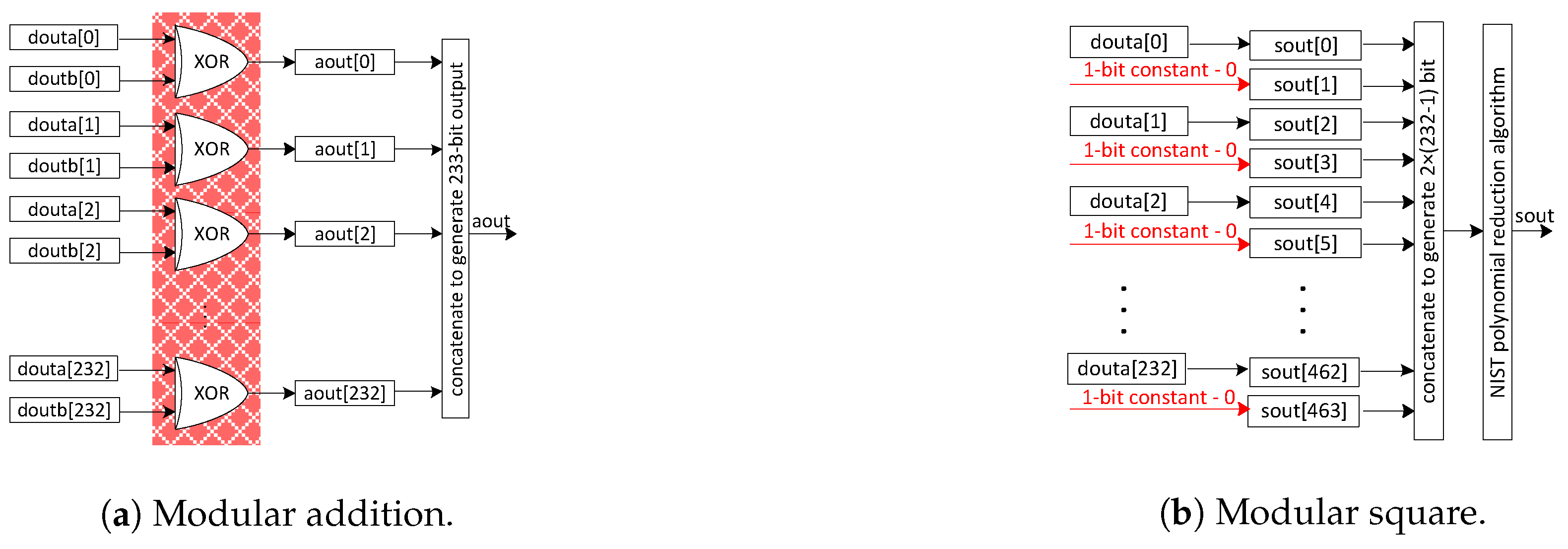
Figure 2a shows the adder unit design, where an array of exclusive-OR gates is needed to implement it—see the red highlighted portion. It takes two 233-bit inputs from the DP-BRAM memory unit and generates a 233-bit accumulated result as the output. The computational cost of the adder circuit is one clock cycle. The modular square over is implemented via the placement of a constant bit ‘0’ after each input data bit, as shown in Figure 2b. It takes one 233-bit input from a DP-BRAM memory unit and produces a 1) bit result as an output. A modular reduction is essential to reduce the squaring result into 233-bit. However, the modular reduction is described later in this paper. Similar to the adder unit, the computational cost of the square unit, including a modular reduction, is one clock cycle.
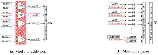
Figure 2.
The internal architectures of adder and square units over field.
3.3.2. Multiplier Unit
The discussion of the multiplier unit is divided into two parts. The first part describes the selection of an appropriate modular multiplier. Subsequently, the second part describes the architecture of the selected modular multiplier.
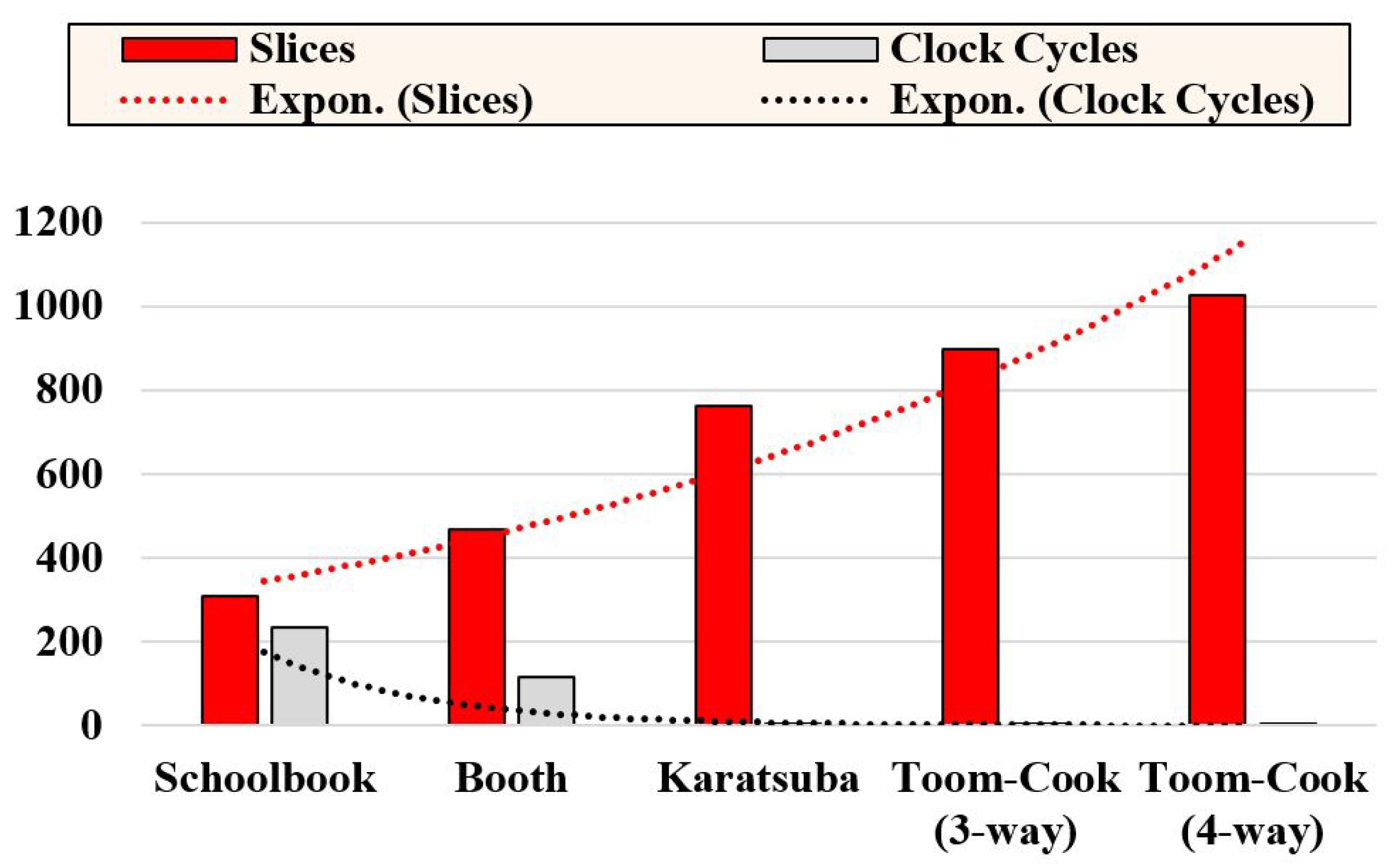
Selection of an appropriate modular multiplier: The modular multiplication operation has significant importance for modular addition and square operations. There are several state-of-the-art polynomial multiplication techniques. Amongst them, the most frequently utilized methods are bit-serial, bit-parallel, digit-serial, and digit-parallel multipliers. Some hardware architectures of these multiplication approaches are reviewed in [32]. Examples of bit-serial multipliers are the schoolbook and booth. Similarly, Karatsuba and Toom–Cook are examples of bit-parallel multipliers. The implementation results of some of these methods are summarized in Figure 3.
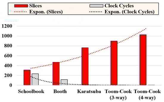
Figure 3.
FPGA slices and clock cycle requirements of bit-serial and bit-parallel polynomial multipliers on Virtex-7 over .
Figure 3 shows that the schoolbook and booth multiplication help to obtain area-optimized designs. However, the computation cost of the schoolbook is m clock cycles for the input operands of m bits. For a similar operand size of m bits, the computation cost of the booth multiplier is clock cycles. On the other hand, bit-parallel and digit-parallel multipliers require one clock cycle with area overhead. Karatsuba and Toom–Cook are examples of bit-parallel multipliers. We do not show the implementation of digit-parallel multipliers in Figure 3. Digit-serial multiplication approaches take clock cycles for one modular multiplication. Here, m is the operand size, and n is the digit size. This method is useful for applications requiring high speed and low-area/power utilizations. Two dotted lines are shown in Figure 3. These lines represent an exponential increase in slices with an exponential decrease in clock cycles. There is always a trade-off between various modular multiplication approaches. Nevertheless, the Karatsuba multiplier needs lower FPGA slices than the Toom–Cook multipliers. Based on the aforementioned observation, a bit-parallel Karatsuba modular multiplier was used in this study. It reduces the overall clock cycles for ECPM computation.
Architecture of our implemented Karatsuba modular multiplier: The Karatsuba multiplier is an efficient way to multiply two polynomials, and it reduces the number of required multiplication operations by splitting a large polynomial’s length into smaller ones. It recursively applies the algorithm to each pair of smaller polynomials and combines the results to obtain the final product. For our implemented Karatsuba multiplier over , each polynomial length is 233 bits, and the polynomial partitions are shown in Figure 4. The gray horizontal bars in Figure 4 show the polynomial splits, and a numerical value inside each circle shows the polynomial size. It is essential to note that it is common in the literature for specific FPGA devices to split Karatsuba polynomials into four levels. After that, the multiplication over smaller split polynomials can be computed using built-in FPGA multipliers. This approach is not compatible with ASIC platforms. Moreover, concerning [33], more polynomial splits result in increased requirement for hardware resources. Therefore, we preferred three polynomial splits in our implemented Karatsuba multiplier, as our implemented multiplier can be used for both FPGA and ASIC platforms. The mathematical background of the Karatsuba multiplier is not presented here; however, interested readers are referred to [12,33] for algorithmic details.
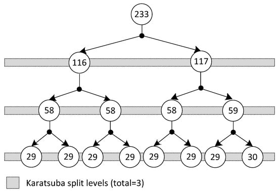
Figure 4.
Polynomial split levels incorporated into the implemented Karatsuba modular multiplier.
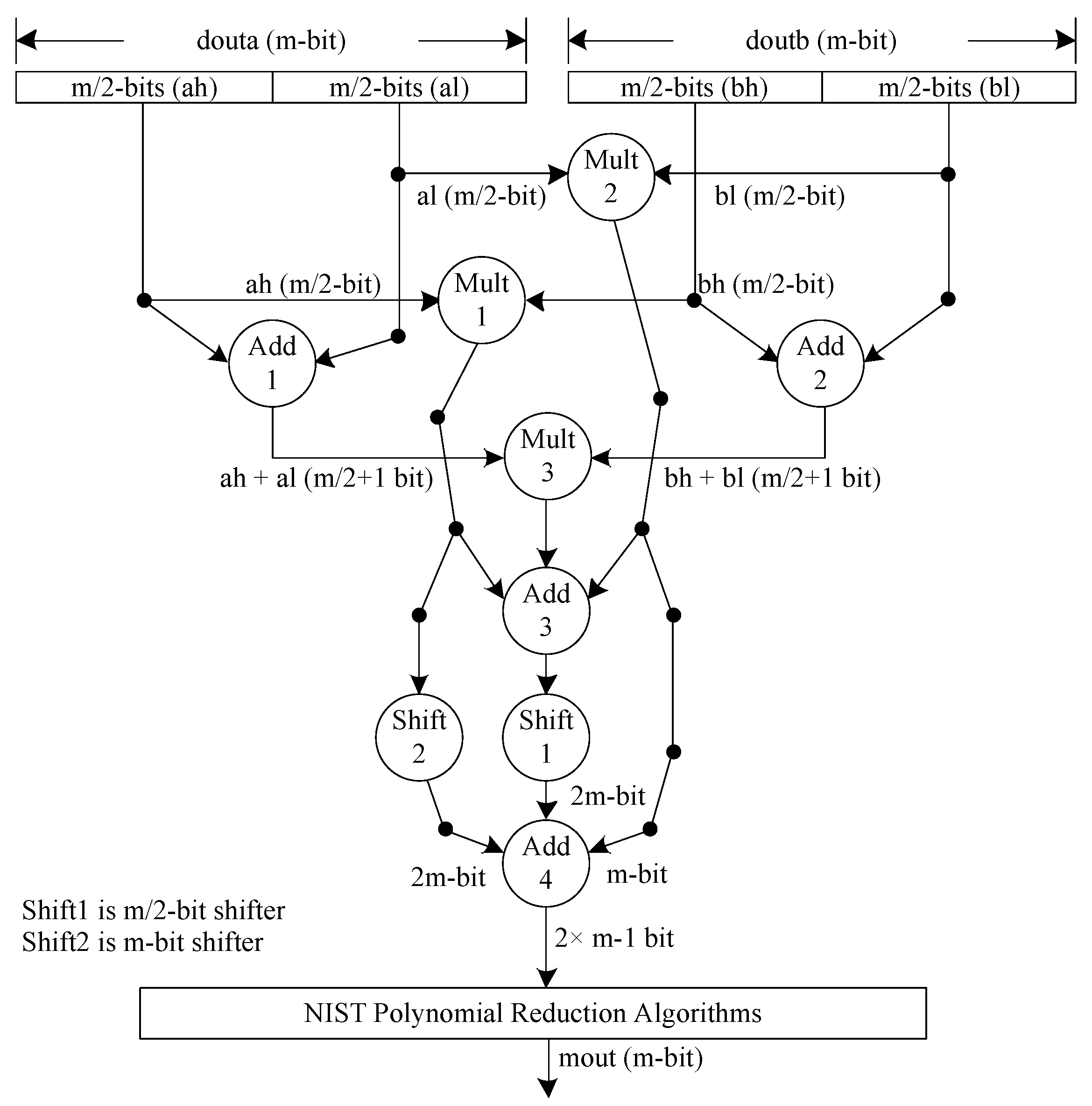
Instead of the polynomial split levels for the Karatsuba multiplier, the complete multiplication architecture is shown in Figure 5, where each polynomial is split into two parts, each of size , resulting in four sub-polynomials, indicated as ‘ah’, ‘al’, ‘bh’, and ‘bl’. The ‘ah’ and ‘al’ are the split polynomials incoming from the douta port of the DP-BRAM memory. Similarly, ‘bh’ and ‘bl’ are the split polynomials incoming from the doutb port of the instantiated memory. Moreover, Figure 5 shows the three inner multiplications required to operate the Karatsuba steps. These include Mult1, Mult2, and Mult3. Mult1 multiplies ‘ah’ and ‘bh’, Mult2 multiplies ‘al’ and ‘bl’, and Mult3 multiplies the outputs generated by adders (i.e., Add1 and Add2). Despite three inner multiplications, four addition operations are also needed to execute Karatsuba multiplication; these include Add1, Add2, Add3, and Add4. Add1 produces a sum of ‘ah’ and ‘al’. Similarly, Add2 adds ‘bh’ and ‘bl’. Add3 produces a sum of the multiplication results generated by multipliers Mult1, Mult2, and Mult3 (as shown in Figure 5). Add4 produces a -bit output. In addition to addition and multiplication operations, two shift operations are also needed, named Shift1 and Shift2. The corresponding Shift1 and Shift2 operators shift the polynomials by and m bits toward the right, respectively, where m is 233.
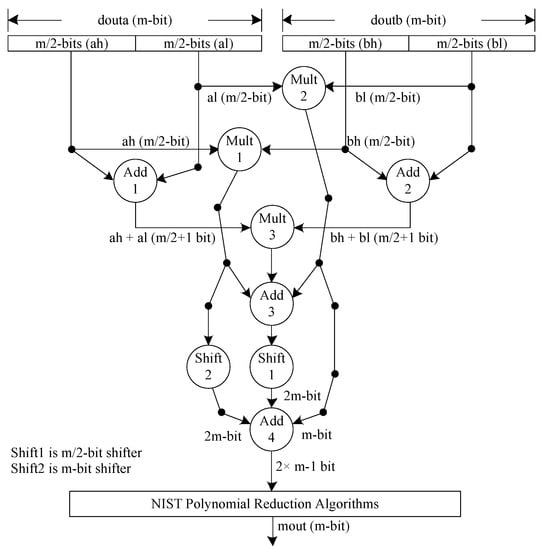
Figure 5.
Architecture of modular multiplier unit over field. Each circle denotes the arithmetic and logical operators such as multiplier, adder, and shifter. A numerical value inside the circle shows the number of operators, which means that three multipliers, four adders, and two shifters are needed to implement the Karatsuba-based polynomial multiplications.
3.3.3. Polynomial Reduction
Figure 2b and Figure 5 show that the polynomial square and multiplier produce output in bits. Therefore, a modular reduction is mandated to generate a polynomial of length m bits. For , we implemented a polynomial reduction algorithm of 2.42 of [3], which requires shift and exclusive-(OR) operations for implementation.
3.3.4. Modular Inversion
Lines 35 and 36 of Algorithm 1 highlight the need for modular inversion computation of ECPM implementation. Multiple approaches exist in the literature to compute modular inversion over . Consequently, the Itoh–Tsujii inversion algorithm is frequently adopted in the literature in ECPM architectures as it needs only squares and modular multiplications for computation. Therefore, an Itoh–Tsujii inversion algorithm was implemented in this study.
In short, Itoh–Tsujii is an efficient method for computing the multiplicative inverse of an element in a binary finite field. It works by expressing the inverse of the element as a polynomial and then using a series of frequent squares and multiplications to compute the inverse of the polynomial [31]. The Itoh–Tsujii method takes 232 squares for a specific field, followed by 10 modular multiplications. Interested readers are referred to [31] for complete algorithmic details.
Concerning hardware implementations, the Itoh–Tsujii algorithm can be implemented in two ways: (i) square Itoh–Tsujii block and (ii) quad Itoh–Tsujii block. The square Itoh–Tsujii version was implemented in [6], allowing one square computation in one clock cycle. In the quad Itoh–Tsujii block, two repeated squares are needed to implement one clock cycle; some hardware implementations are considered in [34,35]. In contrast, the former is well suited for applications that demand area-reduced ECPM implementations with throughput overhead. On the other hand, the latter is suitable for high-speed ECPM computations with area overhead. There is always a trade-off. Hence, to achieve the goal of this study, we implemented the square Itoh–Tsujii algorithm by reusing the existing hardware resources of the square and (Karatsuba) multiplier units, shown in orange in Figure 1. The hardware reutilizations allow us to minimize the hardware resources. Regarding the computational cost of the square Itoh–Tsujii algorithm over , 232 clock cycles are needed for square computations and 10 cycles for multiplication computations.
3.4. Control Unit and Clock Cycles’ Calculation
We implemented an FSM-based dedicated control unit (CU) to execute the control functionalities. The CU is responsible for generating signals that control the routing network (RN) components and the read/write addresses, including the read/write-enable signals for the DP-BRAM unit. The control signals are shown with red and blue dotted lines in Figure 1. Therefore, to implement Algorithm 1, the details of the required clock cycles are described below:
- Affine to projective conversions: The state 0 of the implemented CU is idle, which indicates do not act. The CU generates the control signals for implementing affine to the projective conversion of Algorithm 1 during states 1 to 6. Each state needs one clock cycle for computation; hence, six cycles are needed to implement the affine to projective conversion.
- Point multiplication computation: As shown in Algorithm 1, the ECPM computation in projective coordinates requires 28 instructions: 14 for and 14 for portions. Therefore, to implement these 28 instructions depending on the value of , 29 cycles are required. Out of these 29 cycles, 28 are for implementing 28 instructions of the PA and PD operations of Algorithm 1, while 1 additional clock cycle is necessary to check the value of the and m, where m is a counter that counts the number of points on the specified ECC curve. For with , the value of m increases to 0 when the initial value is . Thus, the PM in projective coordinate takes clock cycles for computation, where m is 233.
- Projective to affine conversion: The projective to affine conversion of the Montgomery ECPM algorithm involves two finite field inversion () computations, as shown in Algorithm 1. We used a single-bit ‘’ signal to monitor these inversion operations. Initially, the ‘’ signal is zero. It remains zero until the completion of the first inversion computation. In the last state of the inversion operation, FSM checks the value of ‘’ signal: if it is 1, the FSM starts generating the control signals for the remaining instructions; otherwise, the FSM sets the ‘’ signal to 1 and starts provoking the control signals to compute the second associated inversion operation. Subsequently, one inversion takes square operations, 10 modular multiplication operations, and utilizes overall clock cycles. Similarly, cycles are needed for two inversion computations. In addition to inversion operations, an additional 18 clock cycles are required to complete the remaining projective to affine conversion instructions of Algorithm 1.
The total clock cycles () for ECPM computation is the sum of clock cycles for an idle state (), affine to projective conversion (), PM executions in projective coordinates (), and projective to affine conversions (). Therefore, the total number of cycles is 7208, which can be calculated using Equation (2):
4. Results and Comparison
Section 4.1 presents the implementation results of the proposed cryptographic processor design. Subsequently, Section 4.2 compares the achieved performance with state-of-the-art designs.
4.1. Results
The proposed hardware architecture was implemented in Verilog HDL using the Vivado IDE tool. The input parameters were selected from the NIST-suggested document [36]. Table 1 provides the implementation results up to the post-place-and-route level on Xilinx devices. Column one shows the implementation devices (Virtex-6 and Virtex-7). Column two provides the total consumed power. Columns three to five show the hardware utilizations in slices, LUTs (look-up tables), and FFs (flip-flops). Similarly, we present the clock cycle, operating frequency, and latency results in columns six to eight. The achieved throughput is shown in column nine; and, finally, the last columns provide the throughput/area ratio. The corresponding power and area values (directly) were obtained from the Vivado tool. The frequency is a reciprocal of the provided time period. It is important to note that there were no timing violations. This implies that the written RTL code for the accelerator is synthesizable and routable. We already described the calculation of the total clock cycles in Section 3.4. The latency determines the time required to perform one ECPM computation. It was calculated using Equation (3). The throughput is the ratio of one over latency and is calculated using Equation (4). Finally, the FoM is defined using Equation (5), where we used slices as the area.

Table 1.
Implementation results after post-place-and-route level of our proposed hardware accelerator over on Xilinx FPGA devices.
The total power consumption of a digital circuit depends on the sum of static and dynamic powers. The static power determines leakage when the device is in idle mode. On the other hand, the dynamic power is related to the switching activity (of the transistors). Multiple approaches are available to measure the dynamic power consumption of the circuit. Amongst others, after the place-and-route level, we report the power results of our accelerator architecture directly from the synthesis tool, i.e., Vivado IDE. As shown in column one in Table 1, the total consumed power of the proposed accelerator design is 0.921 and 0.813 W on Virtex-6 and Virtex-7 devices, respectively. It is noted that the design consumes 11.5% less power on the modern (28 nm) Virtex-7 FPGA compared with that on the older (40 nm) Virtex-6 FPGA. The higher power consumption is due to utilizing a bit-parallel Karatsuba multiplier architecture in the proposed design. A detailed comparison in [37] with different modular multipliers indicates that the bit-parallel multiplication approaches, such as Karatsuba and Toom-Cook, utilize more power than digit-serial and bit-serial modular multiplication methods. Therefore, the power consumption of the hardware design can be minimized by adopting other multiplication methods, i.e., schoolbook and booth, with latency overhead.
Instead of focusing on power consumption, we compared hardware resource utilization (in slices, LUTs, and FFs) of the proposed design on Virtex-7 and Virtex-6 devices. The results are presented in columns three to five in Table 1. The analysis revealed that the proposed design occupies less area on Virtex-7 FPGA than Virtex-6 devices. It shows a significant 23% decrease in slices, LUTs, and FFs when transitioning from Virtex-6 to Virtex-7. This decrease was expected due to the use of different implementation technologies for the two devices. Virtex-6 is built on 40 nm technology, while Virtex-7 is built on more advanced 28 nm technology. Consequently, implementing the same design on different technologies naturally leads to varied hardware costs. Let us break down the Virtex-7 slices of our architecture into its components. The DP-BRAM, the routing network including the control block, and the arithmetic unit consume 31%, 11%, and 58% of the total area. This reveals that the arithmetic unit accounts for more than 50% of the total slices on the Virtex-7 implementation. In the arithmetic unit, the sum of slice utilization for adder and square units is approximately 19%. Similarly, the proposed multiplier unit consumes 39% of the slices. This area expense was expected because the proposed multiplier needs only one clock cycle for implementation. With clock cycles overhead, using modular bit-serial and digit-serial multipliers can optimize the hardware area.
Regarding the timing-related results, column six in Table 1 shows that the proposed design needs 7208 cycles for one ECPM computation. Similar to the designs of [28,30], these clock cycles can be reduced by employing multiple adder, multiplier, and square units with area and power overheads. Another technique is the employment of a quad-block version of the Itoh–Tsujii inversion algorithm, as used in [34,35]. Nevertheless, these optimization approaches increase hardware resources and consumed power. The obtained frequency values are 310 and 350 MHz on Virtex-6 and Virtex-7 FPGA devices, respectively. The proposed accelerator architecture is 13% faster on a modern 28 nm Virtex-7 FPGA than a 40 nm Virtex-6 device. To further improve our architecture’s operating frequency with area and power overheads, it is possible to utilize n-stage pipelining like the ECC accelerators of [6,16,29]. Our architecture requires 23.25 and 20.59 s for one ECPM computation on Virtex-6 and Virtex-7 devices, respectively.
The higher throughput and FoM values ensure an efficient hardware design. The proposed accelerator design can achieve a throughput of 43.01 and 48.56 Kbps on Virtex-6 and Virtex-7 devices. Equation (4) shows that the throughput is a ratio of one over latency. Therefore, the latency values require optimization to maximize the throughput. Several techniques exist (in the literature) to minimize latency. They include pipelining, instruction-level, and design-level parallelism. These methods maximize hardware resources and power values. Hence, we struggled with different design choices to obtain a balanced hardware implementation of the ECPM operation. The calculated FoM values in our design are 9.33 and 13.54 on Virtex-6 and Virtex-7 devices.
4.2. Comparisons
We compared our results with those obtained using state-of-the-art accelerators in Table 2. We implemented the proposed accelerator architecture on various FPGA devices for a fair comparison. Column one in Table 2 shows the reference designs (Ref #). The information on the implementation device is presented in column two. The power consumption is shown in column three. Columns four to six present resource utilization in slices, LUTs, and FFs. The total clock cycle (Tcycles), operating frequency (Freq), and latency (Lat) values are presented in columns seven to nine. The throughput (Thpt) is shown in column ten. Column eleven shows the defined FoM values. Finally, the last column provides the details in terms of implemented ECC model and the supported key length. Power, area, and operating frequency values were obtained directly from the Vivado tool. Latency and throughput values were calculated using Equations (3) and (4), respectively. An FoM value was defined using Equation (5) with slices as the area metric. Moreover, we used the symbol ‘–’ in Table 2 for those where the reference design does not provide the related information.
Table 2.
Comparison with state-of-the-art designs of ECPM hardware accelerators.
Comparison to hardware accelerators of Weierstrass model over [6,12,15]: In comparison with [6], the proposed accelerator achieves a significant reduction in FPGA slices by a ratio of 1.42 (5120 slices in [6] compared with 3584 slices with our method on a similar Virtex-7 FPGA). This reduction is attributed to the implementation of pipelining in [6]. However, Table 2 demonstrates that the pipelined design of [6] requires fewer clock cycles, and computation time, i.e., latency, than our accelerator. In addition, due to pipelining, the operating frequency achieved in [6] is also higher than that of our accelerator. In other words, the two-stage pipelining in [6] enables a shorter critical path, resulting in a higher throughput of 63.37 Kbps, which is 1.30 times greater than our design’s throughput of 48.56 Kbps. Despite our design utilizing fewer hardware resources and the pipelined design of [6] being faster, the overall FoM for our design is 1.09 times higher (ratio of 13.54 with 12.37). This is primarily due to our design’s lower hardware resource utilization, contributing to its improved FoM. Moreover, with a small area overhead, different pipeline stages can be incorporated into our design to accelerate the latency value, which also improves the overall throughput of our design. In short, our design benefits applications that demand throughput/area-optimized ECPM implementations.
In Table 2, the nonpipelined and pipelined ECC implementations of [12] on Artix-7 FPGA reveal that the pipelined architecture is more efficient in operating frequency and computation time, i.e., latency, with area overhead. If we compare the FPGA slices of the pipelined design of [12], our accelerator on Virtex-7 is 1.24 (ratio of 4467 with 3584) times more area-efficient. Also, our accelerator architecture is more area-efficient than the nonpipelined implementation of [12]. This difference is attributed to the combined use of Karatsuba and schoolbook methods in [12], whereas the discussed implementation utilizes only the Karatsuba multiplier. Apart from the area comparison, our accelerator is 24.02 times faster in clock cycles than [12]. The ratio of 173154 to 7208 indicates the relative difference in clock cycles required for modular polynomial multiplication. The improved speed of our design is achieved by using the Karatsuba multiplier, which performs modular polynomial multiplication in a single clock cycle. In contrast, the combined Karatsuba and schoolbook methods in [12] require clock cycles for a singular modular multiplication. Rather than the clock cycles, the proposed accelerator is also faster than nonpipelined and pipelined designs of [12] in operating frequency and latency, as presented in Table 2. Our design’s throughput and FoM values are much higher than those of the nonpipelined and pipelined designs of [12].
On the Virtex-5 FPGA, the design of [15] presents an ECPM architecture for generic irreducible polynomials using a modified Montgomery ladder algorithm. Compared with our method, the design presented in [15] is more efficient regarding clock cycles, latency, and throughput. The reason is that they optimized the finite field inversion operation by employing the modified Itoh–Tsujii algorithm, which helps them to reduce the clock cycles and computation time. In our method, we implemented the square version of the Itoh–Tsujii algorithm using the existing hardware resources of the square and multiplier units, optimizing the overall hardware area. The proposed accelerator utilizes fewer hardware resources, specifically FPGA LUTs, and operates at a higher circuit frequency, as shown in columns five and eight in Table 2. When considering the overall FoM value for comparison, our accelerator is comparatively 1.15 times more efficient than [15].
Comparison with the accelerator of the Weierstrass model over with [17]: On a comparable Virtex-7 FPGA, the hardware resources (in LUTs) presented in [17] exhibit a 1.73-fold increase (a ratio of 23,000 to 13,267) compared with our binary field accelerator. This discrepancy arises from the larger supported key length of 256 in [17], whereas our accelerator supports a 233-bit key length. However, our accelerator surpasses in terms of operating frequency, latency, throughput, and FoM values, as shown in Table 2. It is worth noting that the comparison of power consumption is not feasible as the reference design lacks this information.
Comparison with a four-stage pipelined BHC accelerator over [18]: On a similar Virtex-7 FPGA, the slices of [18] are 1.98 (ratio of 7123 with 3584) times higher than those of the proposed hardware accelerator. Their design incorporates a BHC ECC model, while we employ a Weierstrass model. A comprehensive comparison of various ECC models and PM algorithms was conducted in [2]. It was shown in [2] that the BHC model requires more mathematical instructions than the Weierstrass model. Therefore, the BHC model utilizes more hardware resources. Due to the four-stage pipelining in [18], the circuit frequency of 371 MHz is higher than our non-pipelined hardware accelerator (which is 350 MHz). Overall, the proposed hardware accelerator outperforms in latency, throughput, and FoM results, as shown in Table 2. Regarding the power, our nonpipelined hardware accelerator consumes much lower power than the four-stage pipelined BHC accelerator of [18] which consumes 3481 mW.
In summary, the implementation results of our proposed hardware accelerator on Virtex-5, Virtex-6, and Virtex-7 FPGA devices are shown in Table 1 and Table 2. These results demonstrate the benefits of the accelerator for cryptographic applications requiring both high throughput and efficient utilization of hardware resources. However, it is essential to note that the proposed accelerator is not suitable for applications that demand high-speed cryptographic computations, such as network servers.
5. Conclusions
This paper presented a throughput/area-efficient hardware accelerator design for ECPM computation over on FPGA. Using a bit-parallel Karatsuba multiplier results in reducing clock cycles which eventually helps to optimize throughput. Furthermore, the use of a single modular adder, multiplier, and square block in the arithmetic unit benefits optimizing hardware area. Moreover, the implementation of an Itoh–Tsujii inversion algorithm by leveraging the existing hardware resources of the modular multiplier and square units to perform the multiplicative inverse also helps to reduce the area cost of the design. Consequently, comparison with state-of-the-art methods reveals the suitability of the optimized throughput/area hardware accelerator architecture for various cryptographic applications that demand throughput and area-optimized implementations.
Author Contributions
Conceptualization, M.R., M.Y.I.Z. and M.A.; methodology, S.S.A. and M.R.; software, A.S.; validation, M.R. and M.A.; formal analysis, O.S.S. and M.Y.I.Z.; investigation, M.R. and M.A.; resources, O.S.S.; data curation, A.S.; writing—original draft preparation, A.S. and M.A.; writing—review and editing, M.R. and M.Y.I.Z.; visualization, M.A.; supervision, M.R. All authors have read and agreed to the published version of the manuscript.
Funding
The authors would like to thank the Deanship of Scientific Research at Umm Al-Qura University for supporting this study with grant code: 22UQU4320199DSR01.
Institutional Review Board Statement
Not applicable.
Informed Consent Statement
Not applicable.
Data Availability Statement
Not applicable.
Conflicts of Interest
The authors declare that they have no conflict of interest.
References
- Simsim, M.T. Internet usage and user preferences in Saudi Arabia. J. King Saud Univ.—Eng. Sci. 2011, 23, 101–107. [Google Scholar] [CrossRef]
- Rashid, M.; Imran, M.; Jafri, A.R.; Al-Somani, T.F. Flexible Architectures for Cryptographic Algorithms—A Systematic Literature Review. J. Circuits Syst. Comput. 2019, 28, 1930003. [Google Scholar] [CrossRef]
- Hankerson, D.; Menezes, A.J.; Vanstone, S. Guide to Elliptic Curve Cryptography. 2004; pp. 1–311. Available online: https://link.springer.com/book/10.1007/b97644 (accessed on 27 June 2023).
- Rivest, R.L.; Shamir, A.; Adleman, L. A method for obtaining digital signatures and public-key cryptosystems. Commun. ACM 1978, 21, 120–126. [Google Scholar]
- Miller, V.S. Use of Elliptic Curves in Cryptography. In Advances in Cryptology—CRYPTO ’85 Proceedings; Williams, H.C., Ed.; Springer: Berlin/Heidelberg, Germany, 1986; pp. 417–426. [Google Scholar]
- Imran, M.; Rashid, M.; Jafri, A.R.; Kashif, M. Throughput/area optimised pipelined architecture for elliptic curve crypto processor. IET Comput. Digit. Tech. 2019, 13, 361–368. [Google Scholar] [CrossRef]
- Rashid, M.; Sonbul, O.S.; Arif, M.; Qureshi, F.A.; Alotaibi, S.S.; Sinky, M.H. A Flexible Architecture for Cryptographic Applications: ECC and PRESENT. Comput. Mater. Contin. 2023, 76, 1009–1025. [Google Scholar] [CrossRef]
- Rashid, M.; Sonbul, O.S.; Zia, M.Y.I.; Kafi, N.; Sinky, M.H.; Arif, M. Large Field-Size Elliptic Curve Processor for Area-Constrained Applications. Appl. Sci. 2023, 13, 1240. [Google Scholar] [CrossRef]
- Arif, M.; Sonbul, O.S.; Rashid, M.; Murad, M.; Sinky, M.H. A Unified Point Multiplication Architecture of Weierstrass, Edward and Huff Elliptic Curves on FPGA. Appl. Sci. 2023, 13, 4194. [Google Scholar] [CrossRef]
- He, Z.; Chen, X. Design and implementation of high-speed configurable ECC co-processor. In Proceedings of the 2017 IEEE 12th International Conference on ASIC (ASICON), Guiyang, China, 25–28 October 2017; pp. 734–737. [Google Scholar] [CrossRef]
- Matutino, P.M.; Araújo, J.; Sousa, L.; Chaves, R. Pipelined FPGA coprocessor for elliptic curve cryptography based on residue number system. In Proceedings of the 2017 International Conference on Embedded Computer Systems: Architectures, Modeling, and Simulation (SAMOS), Pythagorion, Greece, 17–20 July 2017; pp. 261–268. [Google Scholar] [CrossRef]
- Kashif, M.; Cicek, I.; Imran, M. A Hardware Efficient Elliptic Curve Accelerator for FPGA Based Cryptographic Applications. In Proceedings of the 2019 11th International Conference on Electrical and Electronics Engineering (ELECO), Bursa, Turkey, 28–30 November 2019; pp. 362–366. [Google Scholar] [CrossRef]
- Zeghid, M.; Ahmed, H.Y.; Chehri, A.; Sghaier, A. Speed/Area-Efficient ECC Processor Implementation Over GF(2m) on FPGA via Novel Algorithm-Architecture Co-Design. IEEE Trans. Very Large Scale Integr. Syst. 2023, 31, 1192–1203. [Google Scholar] [CrossRef]
- Khan, Z.U.A.; Benaissa, M. Throughput/Area-efficient ECC Processor Using Montgomery Point Multiplication on FPGA. IEEE Trans. Circuits Syst. II Express Briefs 2015, 62, 1078–1082. [Google Scholar] [CrossRef]
- Nadikuda, P.K.G.; Boppana, L. An area-time efficient point-multiplication architecture for ECC over GF(2m) using polynomial basis. Microprocess. Microsyst. 2022, 91, 104525. [Google Scholar] [CrossRef]
- Imran, M.; Pagliarini, S.; Rashid, M. An Area Aware Accelerator for Elliptic Curve Point Multiplication. In Proceedings of the 2020 27th IEEE International Conference on Electronics, Circuits and Systems (ICECS), Scotland, UK, 23–25 November 2020; pp. 1–4. [Google Scholar] [CrossRef]
- Wang, D.; Lin, Y.; Hu, J.; Zhang, C.; Zhong, Q. FPGA Implementation for Elliptic Curve Cryptography Algorithm and Circuit with High Efficiency and Low Delay for IoT Applications. Micromachines 2023, 14, 1037. [Google Scholar] [CrossRef]
- Rashid, M.; Imran, M.; Kashif, M.; Sajid, A. An Optimized Architecture for Binary Huff Curves with Improved Security. IEEE Access 2021, 9, 88498–88511. [Google Scholar] [CrossRef]
- Jafri, A.R.; Ul Islam, M.N.; Imran, M.; Rashid, M. Towards an optimized architecture for unified binary huff curves. J. Circuits Syst. Comput. 2017, 26, 1750178. [Google Scholar] [CrossRef]
- Bedoui, M.; Bouallegue, B.; Ahmed, A.M.; Hamdi, B.; Machhout, M.; Mahmoud; Khattab, M. A secure hardware implementation for elliptic curve digital signature algorithm. Comput. Syst. Sci. Eng. 2023, 44, 2177–2193. [Google Scholar] [CrossRef]
- Trujillo-Olaya, V.; Velasco-Medina, J. Hardware implementation of elliptic curve digital signature algorithm over GF(2409) using sha-3. Int. J. Mach. Learn. Comput. 2022, 12, 73–78. [Google Scholar] [CrossRef]
- Khan, S.Z.; Jamal, S.S.; Sajid, A.; Rashid, M. FPGA implementation of elliptic-curve diffie hellman protocol. Comput. Mater. Contin. 2022, 73, 1879–1894. [Google Scholar] [CrossRef]
- FIPS. Digital Signature Standard—Publication 186-5 (Supersedes FIPS 186-4). 2023. Available online: https://doi.org/10.6028/NIST.FIPS.186-5 (accessed on 29 June 2023).
- Barker, E.; Chen, L.; Roginsky, A.; Smid, M. Recommendation for Pair-Wise Key Establishment Schemes Using Discrete Logarithm Cryptography. 2023. NIST Special Publication 800-56A (Revision 2). Available online: http://dx.doi.org/10.6028/NIST.SP.800-56Ar2 (accessed on 16 June 2023).
- Singh, A.; Gutub, A.; Nayyar, A.; Khan, M.K. Redefining food safety traceability system through blockchain: Findings, challenges and open issues. Multimed. Tools Appl. 2023, 82, 21243–21277. [Google Scholar] [CrossRef]
- Almotairi, K.H. Application of internet of things in healthcare domain. J. Umm Al-Qura Univ. Eng. Archit. 2023, 14, 1–12. [Google Scholar] [CrossRef]
- Khan, F.; Jan, M.A.; Alturki, R.; Alshehri, M.D.; Shah, S.T.; Rehman, A.U. A Secure Ensemble Learning-Based Fog-Cloud Approach for Cyberattack Detection in IoMT. IEEE Trans. Ind. Inform. 2023, 19, 10125–10132. [Google Scholar] [CrossRef]
- Khan, Z.U.A.; Benaissa, M. High-Speed and Low-Latency ECC Processor Implementation Over GF( 2m) on FPGA. IEEE Trans. Very Large Scale Integr. Syst. 2017, 25, 165–176. [Google Scholar] [CrossRef]
- Al-Khaleel, O.; Papachristou, C.; Wolff, F.; Pekmestzi, K. An Elliptic Curve Cryptosystem Design Based on FPGA Pipeline Folding. In Proceedings of the 13th IEEE International On-Line Testing Symposium (IOLTS 2007), Crete, Greece, 8–11 July 2007; pp. 71–78. [Google Scholar] [CrossRef]
- Lai, J.Y.; Hung, T.Y.; Yang, K.H.; Huang, C.T. High-performance architecture for Elliptic Curve Cryptography over binary field. In Proceedings of the 2010 IEEE International Symposium on Circuits and Systems, Paris, France, 30 May–2 June 2010; pp. 3933–3936. [Google Scholar] [CrossRef]
- Itoh, T.; Tsujii, S. A fast algorithm for computing multiplicative inverses in GF(2m) using normal bases. Inf. Comput. 1988, 78, 171–177. [Google Scholar] [CrossRef]
- Imran, M.; Rashid, M. Architectural review of polynomial bases finite field multipliers over GF(2m). In Proceedings of the 2017 International Conference on Communication, Computing and Digital Systems (C-CODE), Islamabad, Pakistan, 8–9 March 2017; pp. 331–336. [Google Scholar] [CrossRef]
- Kang, B.; Cho, H. FlexKA: A Flexible Karatsuba Multiplier Hardware Architecture for Variable-Sized Large Integers. IEEE Access 2023, 11, 55212–55222. [Google Scholar] [CrossRef]
- Kalaiarasi, M.; Venkatasubramani, V.R.; Rajaram, S. A Parallel Quad Itoh-Tsujii Multiplicative Inversion Algorithm for FPGA Platforms. In Proceedings of the 2020 Third ISEA Conference on Security and Privacy (ISEA-ISAP), Guwahati, India, 27 February–1 March 2020; pp. 31–35. [Google Scholar] [CrossRef]
- Kalaiarasi, M.; Venkatasubramani, V.; Manikandan, M.; Rajaram, S. High performance HITA based Binary Edward Curve Crypto processor for FPGA platforms. J. Parallel Distrib. Comput. 2023, 178, 56–68. [Google Scholar] [CrossRef]
- NIST. Recommended Elliptic Curves for Federal Government Use (1999). Available online: https://csrc.nist.gov/csrc/media/publications/fips/186/2/archive/2000-01-27/documents/fips186-2.pdf (accessed on 22 May 2023).
- Imran, M.; Abideen, Z.U.; Pagliarini, S. A Versatile and Flexible Multiplier Generator for Large Integer Polynomials. J. Hardw. Syst. Secur. 2023. [Google Scholar] [CrossRef]


Disclaimer/Publisher’s Note: The statements, opinions and data contained in all publications are solely those of the individual author(s) and contributor(s) and not of MDPI and/or the editor(s). MDPI and/or the editor(s) disclaim responsibility for any injury to people or property resulting from any ideas, methods, instructions or products referred to in the content. |
© 2023 by the authors. Licensee MDPI, Basel, Switzerland. This article is an open access article distributed under the terms and conditions of the Creative Commons Attribution (CC BY) license (https://creativecommons.org/licenses/by/4.0/).