Abstract
Ultra-wideband (UWB) antennas cover a frequency range of 3.1 to 10.6 GHz and have sparked a lot of research interest as an essential part of wireless communication systems as they provide high data transmission speeds, are less expensive, and consume less power. UWB antennas are widely used in radar imaging, radio frequency identification, public security, and other high-accuracy positioning devices such as altimetry. Some smart applications of UWB antennas are vehicular radar systems, surveillance systems, software-defined radios, spectrum analysis, proximity fuses, etc. Multiple-input-multiple-output (MIMO) is a multiplexing technology that adopts multiple antennas both at the transmitter and receiver, which can enhance the channel capacity. MIMO technology is extensively used in several applications, such as in portable devices, wireless body area networks (WBANs), vehicular communication, and satellite–terrestrial networks. Generally, the MIMO antennas are used to obtain high reliability, high capacity, high throughput, and high security. The UWB MIMO antennas (UMAs) are considered the best choice for wireless communication systems as they offer reliability and wide transmission capacity, in contrast to unit antenna elements (AEs), without increasing system bandwidth or transmission power. The present-day and future communications systems need higher throughput to meet the demands of users. The signal transfer rate can be improved by improving channel bandwidth or increasing the number of receiving antennas. However, the main issue in designing UMAs is to provide high isolation between AEs because mutual coupling interactions between them affect the generated radiation patterns, leading to worse performance and failing to meet the operative constraints and requirements. When introducing decoupling techniques (DTs), researchers experience numerous challenges, including an increase in antenna size, design complexity, and cross-polarization. This article offers an organized review and simulated study of the various DTs in UMAs. The simulated study has been carried out through the implementation of various types of DTs on the same two-port UMA, which consists of two microstrip-fed circular-shaped AEs with open-end slotted partial ground. In contrast with previously reported review articles, this article provides a detailed study of various types of DTs reported so far and a better understanding for selecting appropriate DTs, which help in designing UMAs with better performance.
1. Introduction
Ultra-wideband (UWB) antennas have sparked a lot of current research interest as they are an essential element in wireless communication systems. Of late, UWB communication technologies have been studied to fulfill the demand for high data speed, low cost, and low power [1]. The planar antennas are turning out to be more popular for UWB applications after the Federal Communications Commission (FCC) assigned UWB an unlicensed frequency range from 3.1 GHz to 10.6 GHz [2]. For emerging UWB wireless applications, printed slots and monopole-type antennas are used because of their simple realization, satisfactory frequency response, and easy integration with other active devices [3]. UWB antennas are widely used in radar imaging, radio frequency identification [4], public security, and device positioning. Some smart applications of UWB antennas include vehicular radar systems, surveillance systems, software-defined radios, spectrum analysis, and proximity fuses [4]. Some research problems in UWB antennas include wide impedance matching, radiation stability, low profile, small size, and reasonable cost [5].
Multiple-input-multiple-output (MIMO) is a multiplexing technology with multiple antennas both on the transmitter and receiver, which can enhance the channel capacity by making full use of the rich scattering environment without sacrificing additional spectrum or power [6,7,8]. MIMO antennas are used to achieve a high capacity and throughput [9]. In the last decade, many research papers that investigated the performance of MIMO systems for satellite–terrestrial networks have been published. In article [10], a secrecy-energy efficient hybrid beamforming (BF) scheme was investigated, wherein a multibeam satellite (MS) system shared the mm-wave spectrum with a cellular system. Under the assumption of imperfect angles of departure for the wiretap channels, the hybrid beamformer at the base station and digital beamformers at the satellite were jointly designed. In [11], a joint beamforming design and optimization for reconfigurable intelligent surface-aided hybrid satellite–terrestrial relay networks were reported, where the links from the satellite and base station (BS) to multiple users were blocked. In [12], a low-complexity optimization framework in terms of secrecy-energy efficiency beamforming for MS systems was developed. An alternating optimization scheme using the signal-to-leakage-plus-noise ratio criterion and successive convex approximation method to iteratively obtain closed-form beamforming weight and power allocation factors was presented. In [13], the physical layer security of a satellite network was investigated, whose downlink spectral resource was shared with a terrestrial cellular network. A multi-antenna BS was proposed as a source of green interference to enhance secure transmission, with the assumption that imperfect channel state information (CSI) and statistical CSI of the link between the BS and satellite user are available at the BS.
In multi-antenna wireless communication systems, precoding has to be studied to simultaneously support data transmission to multiple users to reduce the interference prior to transmission and achieve the channel capacity [14]. The antenna system with a beam scanning capability can filter the interference of other channels by targeting the radiation pattern in a specific direction to obtain more stable data transmission [15]. For secure MIMO transmission in a mobile vehicular network, a wireless-powered communication with integrated MIMO technology for radio frequency energy harvesting was presented [16]. Massive MIMO and mm-wave MIMO are considered to be the key enablers for fifth-generation (5G) wireless networks. By exploiting the sparsity of mm-wave channels, the corresponding channel estimation can significantly reduce the required pilot overhead. It is particularly beneficial to mm-wave MIMO systems, where the number of pilot symbols increases linearly with the number of reflecting elements and transmit antennas [17]. Massive MIMO is an attractive technology to support the desired 1000-fold system throughput improvements for 5G cellular communication systems [18]. In recent years, with the growing demand for higher data rates in post-5G mobile communications, mm-wave bands have received considerable research interest [19,20,21]. Recently, the mm-wave bandpass filters (BPFs) have attracted significant attention with the development of 5G systems [22]. Also, waveguide directional couplers are widely used in microwave and mm-wave systems [23]. Integrating a MIMO antenna and a substrate-integrated waveguide BPF in a single quarter/quintuple mode cavity can significantly reduce the overall loss, cost, and complexity of front-end systems and have potential applications in contemporary wireless communication devices [24,25].
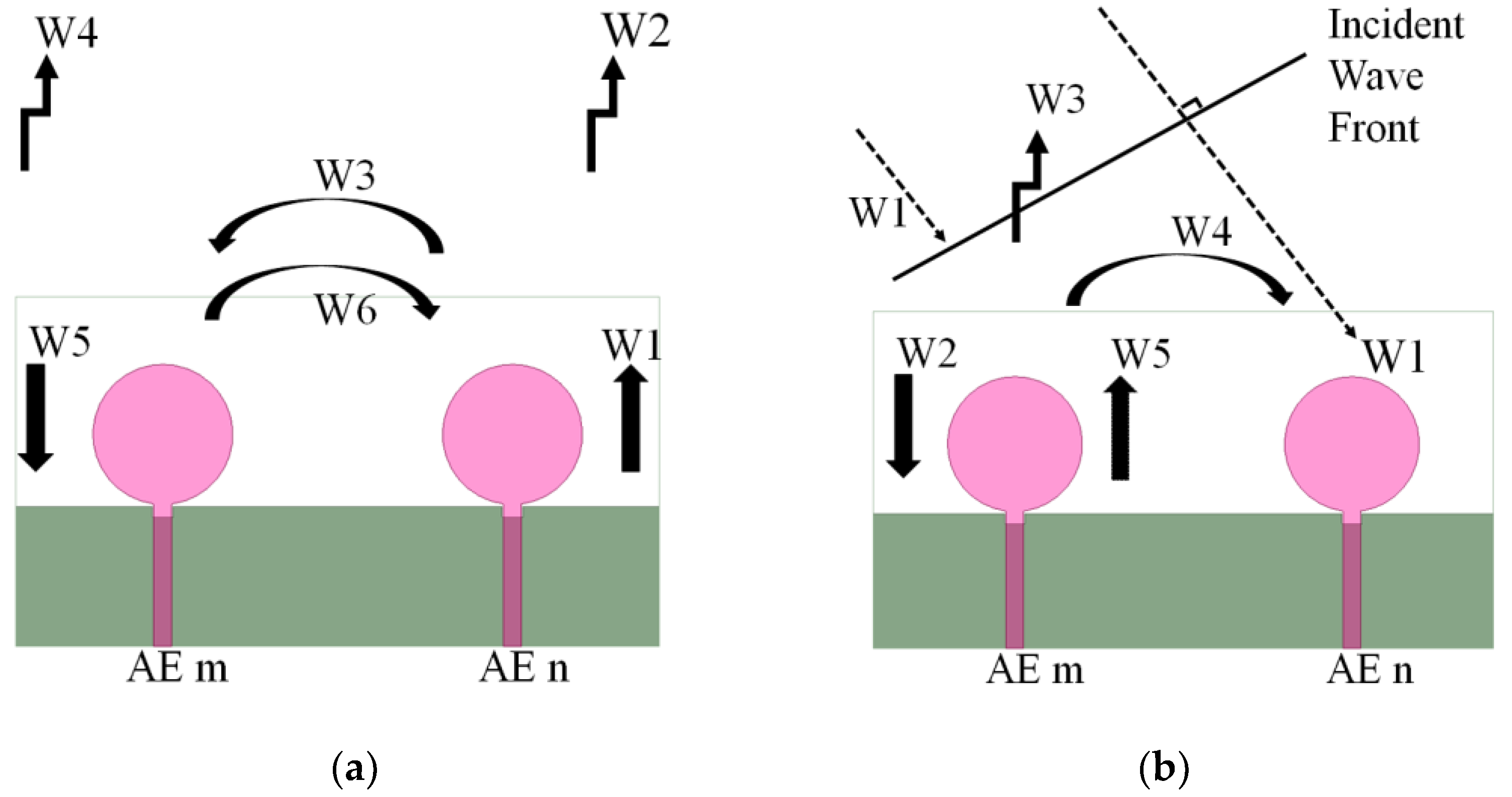
The diversity performance of the MIMO antenna is evaluated by the low envelope correlation coefficient (ECC) and high isolation between/among ports. These two factors are greatly affected by the distance between the antenna elements (AEs) [3]. The main problem with UWB MIMO antennas (UMAs) is the high mutual coupling between closely spaced AEs. The energy consumed by neighboring AEs when one AE is working depicts the mutual coupling. In general, the modification in impedance matching, reflection coefficients, and far-field radiation patterns of the AEs are consequences of the high mutual coupling. Practically, the mutual coupling relies upon the MIMO design and on the excitations of other nearby AEs. The systems of mutual coupling rely on the transmitting/receiving mode [26]. To explain this, two AEs m and n in the MIMO antenna are presented in Figure 1a,b in both transmitting and receiving modes, respectively. In the transmitting mode, AE n is energized as W1. This energy radiates into space as W2, and toward the AE m as W3. The AE m rescatters part of the energy into space as W4, and the remaining goes toward the port as W5. The AE n obtains a small part of the rescattered energy W4 as W6. This cycle of mutual coupling will go on endlessly. However, because of the significant decrease in rescattered energy at each iteration, it is desirable to consider the first few iterations. Therefore, total far-field radiation is a vector sum of the rescattered and radiated far-fields. This shows that the antenna radiation pattern is modified due to high mutual coupling. The wave W5 connects vectorially to the reflected and incident waves of the AE m. This enhances the standing plane wave, which in turn alters the impedance matching of the AE m. The mutual coupling modifies the mutual input impedance as well as antenna self-impedance. In the transmitting mode, various ports of a MIMO antenna may have arbitrary phase excitations. This will affect both the mutual coupling and the impedance matching of AEs.
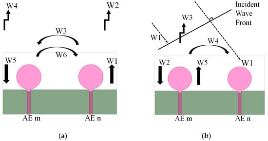
Figure 1.
Mutual coupling in (a) transmitting mode and (b) receiving mode. {Note: W = Wave}.
If a wave W1 encroaches onto the MIMO antenna in receiving mode, reaching first at the mth AE, it first instigates a current in the AE m. Some portion of the incident plane wave goes into the AE m as W2, while its portion is re-scattered into space as W3. A portion of the re-scattered plane wave is coordinated toward the AE n as W4, where it combines vectorially with the incident plane wave W1. Henceforth, the plane wave received by an AE is the vector addition of the coupled waves and the direct waves from other neighboring AEs. To limit the re-scattered energy or boost the received energy, the terminating load impedance of the AE m ought to be picked so that the reflected wave W5 cancels the re-scattered wave W3. The AE performance is determined by the excitation of one AE and the termination of other AE/s with 50 Ω load/s in the receiving mode. There are a number of challenges faced by the researchers to improve isolation between closely spaced AEs. The mutual coupling interactions between AEs affect the generated radiation patterns, leading to worse performance and failure to meet the operative constraints and requirements [27]. The demand for high-density integrated circuits has propelled research into the innovative designs of compact antennas with high performance [28]. It is a challenge to provide high isolation within closely spaced AEs. And, by introducing any decoupling technique (DT), the overall size of the MIMO antenna may increase. In the case of UMAs, isolation needs to be higher throughout the UWB range. Also, antenna design becomes complex and even high cross-polarization is obtained. Hence, the careful design of a DT in a MIMO antenna that does not degrade its performance is required.
There are a number of reasons due to which the UWB antenna is combined with MIMO technology. And, to achieve more than 50 Mb/s data rates, technologies such as MIMO and orthogonal frequency-division multiplexing (OFDM) can be adopted, as recommended in IEEE 802.11n. To reach the target of 1 Gb/s, more advanced techniques should be used. The UWB technology combined with MIMO could provide a solution to this issue [7]. Due to the regulation imposed by the FCC, the permitted power spectral density of the UWB signal is rather limited. This again limits data transmission rates. Incorporating the MIMO technique into UWB provides a viable solution for the restricted access problem of power limitation [29]. The channel capacity of UWB systems is proportional to the number of transmit/receive antennas, and data rates can be significantly further increased through the combination of UWB and MIMO [30].
Some review papers on UMAs were published in the past, as displayed in Table 1. However, in [31,32], DTs were not explained, and in [33,34], only a few DTs were discussed. A detailed analysis of DTs was not performed in [35]. The literature survey in [36] was not focused on UMAs. The following are the main highlights of this review article:

Table 1.
Main contributions of previously reported articles and the presented review article.
- In the proposed review article, all DTs for UMAs are analyzed in detail. This analysis will help the new researchers to understand all DTs.
- Various parameters of the reported UMAs are examined, such as antenna size, substrate used, isolation, bandwidth, and gain. This investigation provides shortcomings of the previously reported UMAs.
- A simulated study of all DTs has been carried out through the implementation of various types of DTs on the same two-port UMA, which consists of two microstrip-fed circular-shaped AEs with an open-end-slotted partial ground. This study determines the effect of applying various DTs on antenna parameters, such as impedance matching, isolation, and radiation pattern.
- A comparative analysis of various DTs has been carried out both with and without common ground (CG). Using this analysis, one can determine the best DT to obtain better isolation.
- This article can save time for the researchers to select appropriate DT without compromising the antenna performance.
2. Decoupling Techniques (DTs) in Ultra-Wideband MIMO Antennas (UMAs)
Various DTs to reduce mutual coupling are presented in the literature. For example, placing AEs at 90 [37,38,39,40,41,42,43,44,45,46] and 180 [47,48,49], introducing DS [50,51,52,53,54,55,56,57,58,59], NL [60,61], DGS [62,63,64], metamaterial [65,66,67], PE [68,69,70], CBF [71], and SES [72].
2.1. Placing AEs at 90 and 180
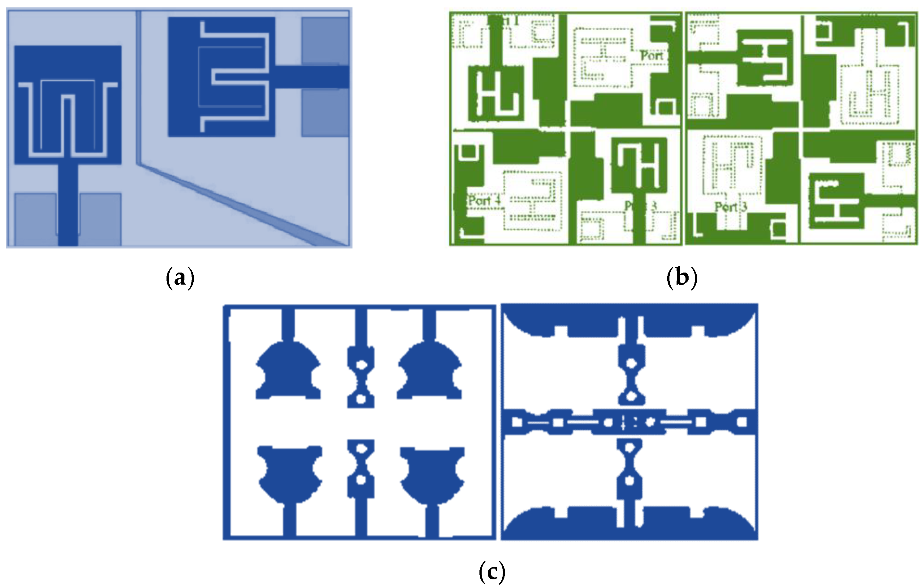
By locating AEs at an angle of 90 (orthogonal), isolation between AEs can be increased. In the literature survey of UMAs, the arrangement of AEs is mostly orthogonal. In [37], a sector was detached from a circular patch of the AE to improve impedance bandwidth, and a U-slot was added in the patch to reject interference from the Wi-MAX band, as presented in Figure 2a. For isolation of the MIMO antenna, the AEs were placed orthogonally and had separated ground planes to achieve greater isolation. In [38], the single AE contained a semi-circular patch and a triangular-shaped truncated ground surface, as displayed in Figure 2b. The upper corners of the ground plane were triangularly truncated to receive better impedance matching. Here, good isolation was obtained by just locating the AEs orthogonally. In [39], the circular patch was loaded with four circular slots of different radii, where the center of the circular slot coincides with the external edge of the circular disk, as shown in Figure 2c. The truncated corners of the ground planes were used for wideband matching. The four AEs were placed orthogonally to increase isolation. In reference [40], the AE consisted of a half-elliptical monopole patch on the upper side with a counterpart half-elliptical slot added to the ground surface, as presented in Figure 2d, which was called the quasi-self complementary (QSC) method. The antenna was excited by a tapered transmission line to achieve wide bandwidth. In the four-port MIMO structure, the isolation was enhanced by the orthogonal arrangement of the AEs. A C-slot was added to the semi-elliptical radiator to suppress the WLAN band. In paper [41], the antenna was designed using step etching on the ground plane, and an arrow-shaped slot was loaded on the radiating patch to enhance bandwidth, as displayed in Figure 2e. The homogeneous elements and angular variation techniques were applied to reduce mutual coupling between AEs. In reference [42], the antenna consisted of four monopole AEs, where each monopole had three concentric rings, as presented in Figure 2f. The orthogonal arrangement of the AEs provided good isolation and polarization diversity. In [43], the AE was designed using modified elliptical radiators, as shown in Figure 2g. The AE was further developed into a MIMO antenna configuration with four elements placed orthogonally to each other in a single plane. In paper [44], the MIMO antenna was composed of four octagonal-shaped radiators with several slots loaded into them, which were placed orthogonally, as displayed in Figure 2h. In [45], the AE consisted of a circular patch that offers better impedance matching over the UWB range without the use of a feeding line, as shown in Figure 2i. The four AEs were arranged across the four edges of a common square-shaped ground to design the MIMO antenna. In [46], a coplanar waveguide (CPW)-fed quasi-elliptical-self complementary antenna exhibiting super-wideband characteristics with dual-band notches was presented. In order to achieve better inter-element isolation and polarization diversity, the four radiating elements of the MIMO antenna were placed orthogonally to each other. Each MIMO antenna element had an elliptical-shaped conductor patch and a slot, which was a complement of similar shape, both present on the same side of the substrate, as displayed in Figure 2j.
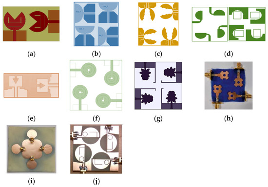
Figure 2.
AEs placed orthogonally: (a) [37], (b) [38], (c) [39], (d) [40], (e) [41], (f) [42], (g) [43], (h) [44], (i) [45], and (j) [46].
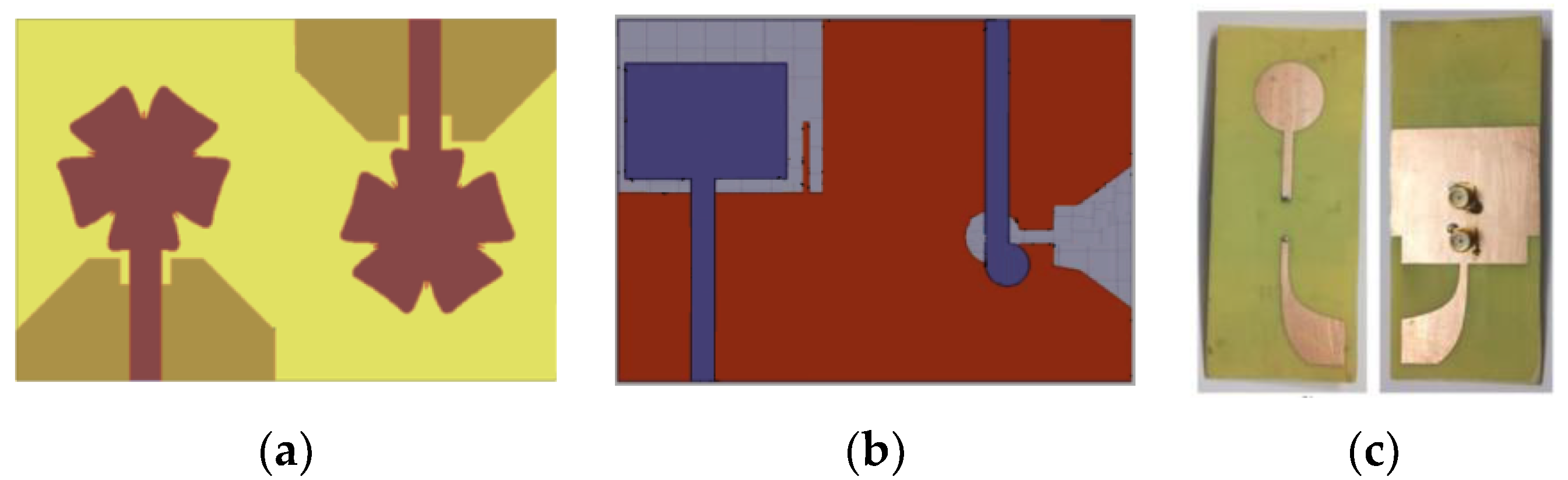
The isolation can also be improved by placing AEs at a 180 rotation. In the literature survey, many UMAs were designed with 180 rotation. In reference [47], the AE had a flower-shaped patch with microstrip feeding, as displayed in Figure 3a. The edges of the ground were chamfered, and an open-end slot was inserted near the feeding point for bandwidth improvement. The AEs were placed at 180 to each other to obtain high isolation. In reference [48], a two-port UMA was designed, where the first AE consisted of a rectangular patch and the second AE had a tapered slot, which were fed by two microstrip lines, as shown in Figure 3b. To improve impedance matching, a circular coupling design was used to feed the slot antenna. The parasitic resonance was produced by a ground stub, which helped enhance the bandwidth of the monopole AE. High isolation was obtained by just placing AEs in a 180 location. In the article [49], the MIMO antenna was composed of dual UWB-based AEs. The antipodal Vivaldi and circular-shaped monopole element were positioned on the two opposite edges of the rectangular-shaped ground surface, as presented in Figure 3c. The two AEs were able to stimulate distinct modes on the ground surface, resulting in the required distinct radiation (far-field) patterns and highly isolated AEs.
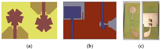
Figure 3.
AEs placed in 180 orientation: (a) [47], (b) [48], and (c) [49].
2.2. Decoupling Structure (DS)
In this DT, a conducting decoupling stub-like structure is attached to the CG between AEs to enhance isolation. In reference [50], the antenna involving an open annular slot (monopole-like) and two indistinguishable CPW strips ending in a U-shaped stub was proposed, as illustrated in Figure 4a. High isolation was accomplished using a diagonally integrated strip in the ground, which increases the current path between AEs. The ground plane was designed as an open annular-like slot, which decreased the size of the antenna. Likewise, an impedance transformer (one-stage) was fused into the CPW transmission line to improve matching. The feeding structure (U-shaped) gave a compelling coupling between the feeding and the slot. An arc-slot resonator was etched on the U-shaped stubs to obtain notch bands. In reference [51], the antenna contained two CPW-feed modified staircase radiating patches with orthogonal directed radiation patterns. A quarter circular slot was added to the ground surface, and a rectangular stub was located at 45° between two AEs, which not only extended the current path but also provided high isolation, as shown in Figure 4b. By adding two slots in the patch radiators, a band-notched performance was achieved at 5.5 GHz.
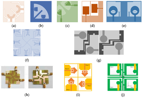
Figure 4.
Decoupling structure: (a) [50], (b) [51], (c) [52], (d) [53], (e) [54], (f) [55], (g) [56], (h) [57], (i) [58], and (j) [59].
In [52], each AE contained a half fan-shaped radiator with a complimentary cut in the ground, as presented in Figure 4c. The AEs were positioned orthogonally to obtain polarization diversity. In this design, high isolation was attained by adding an arrow-like stub to the ground. A notched band for WLAN was designed by adding a bent slit in each radiator. In reference [53], the antenna was composed of dual identical CPW-fed rectangular radiators, as displayed in Figure 4d. To reduce mutual coupling as well as to expand bandwidth, a rectangular strip was added to the ground surface. To reject the WLAN band, an inverted U-slot was introduced in the feed line. In reference [54], the AE consisted of a circular radiator in which the eye slot was etched to achieve a better impedance bandwidth, as displayed in Figure 4e. The microstrip line feeding was connected at the lower ends of each radiator. The two AEs have a common rectangular-shaped ground located beneath the radiating AEs to maintain the compactness of the designed antenna. Furthermore, the ground was modified via the addition of a T-shaped stub to achieve better isolation between the two radiators.
The antenna in [55] had a modified substrate geometry and was composed of a circular arc-shaped conductive element on top, as shown in Figure 4f. Polarization diversity and isolation were achieved by replicating the elements orthogonally, forming a plus-shaped structure. The modified ground plane consisted of an inverted L-shaped strip and a semi-ellipse slot over the partial ground that helped the antenna achieve wide bandwidth. In paper [56], the antenna consisted of four symmetric circular elements with a slotted ground plane, as shown in Figure 4g. The two sides of the substrate were symmetrical, and each side consisted of two radiators with partial ground planes associated with the two other elements mounted on the other side. The two AEs of the front side were orthogonal to the two other elements of the back side in order to increase the isolation between elements. For further reduction in the coupling between AEs, decoupling structures were presented in the top and bottom layers of the substrate. In [57], the MIMO antenna contained four monopole AEs with rectangular radiators, each fed via an L-shaped microstrip line, as displayed in Figure 4h. The high isolation was accomplished via the orthogonal direction of AEs and a cross-shaped DS. The designed antenna can realize WLAN and X-band NBs by etching two C-shaped slits from each radiator and Wi-MAX NB by introducing an L-shaped slit in the ground. In reference [58], the MIMO antenna was composed of four identical rhombic-shaped monopole radiators arranged orthogonally, as shown in Figure 4i. To eliminate Wi-MAX and WLAN bands from the UWB range, the antenna radiators were loaded with elliptical CSRR structures, and to achieve high isolation, a plus-shaped DS was added. In [59], the MIMO antenna consisted of four AEs, each composed of a microstrip feed line and a square-slotted ground plane. A circular stub protruded from the ground plane strip to achieve circular polarization, as shown in Figure 4j. Also, a rectangular-shaped strip was integrated into the antenna ground surface to achieve good isolation between antenna ports.
2.3. Neutralization Line (NL)
In this DT, NL is attached to the two AEs to enhance isolation. This produces the extra current path between the dual AEs of the MIMO antenna. In reference [60], a semi-circular patch was combined with a modified rectangular patch to design the AE, as shown in Figure 5a. A pair of antennas were combined with the NL to improve the isolation between the two ports. In [61], two AEs had a circular patch with a microstrip feed line. An NL was inserted between two AEs. The NL consisted of two conducting strips and a circular disc, as shown in Figure 5b. The circular disc allowed several possible decoupling current paths with different lengths to cancel the coupling current on the ground plane. Hence, wideband isolation was achieved.
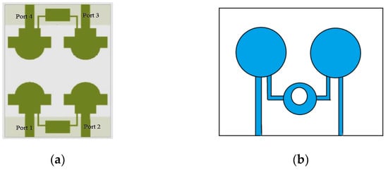
Figure 5.
Neutralization line: (a) [60] and (b) [61].
2.4. Defected Ground Structure (DGS)
In this DT, by introducing various types of slits/slots in the ground surface, isolation is improved. This expands the path of the current to reduce the first resonance frequency and suppresses the surface currents to enhance isolation. In [62], the AE containing a T-shaped stub was connected to a rectangular patch for bandwidth enhancement, as presented in Figure 6a. The AEs were placed orthogonally to each other. Also, the antenna contained two open slots in the ground, which were located perpendicularly to each other to achieve high isolation. To further enhance the isolation between AEs, a narrow rectangular slot with a length of λg/4 was cut into the ground surface. In reference [63], a Vivaldi MIMO antenna was presented with a modified ground surface and two microstrip line feedings, as shown in Figure 6b. By adding a T-slot in the ground, port isolation was significantly increased. By adding two SRRs of different sizes, dual notched bands were obtained to filter the interference of WLAN and satellite-based X-band. In reference [64], the antenna consisted of dual CPW-fed V-like parallel and symmetric radiators, as shown in Figure 6c. The T-slot was added on the ground plane to enhance isolation and increase the bandwidth. The radiator shape had a smooth transition of currents from the CPW feed line to the radiator.

Figure 6.
Defected ground structure: (a) [62], (b) [63], and (c) [64].
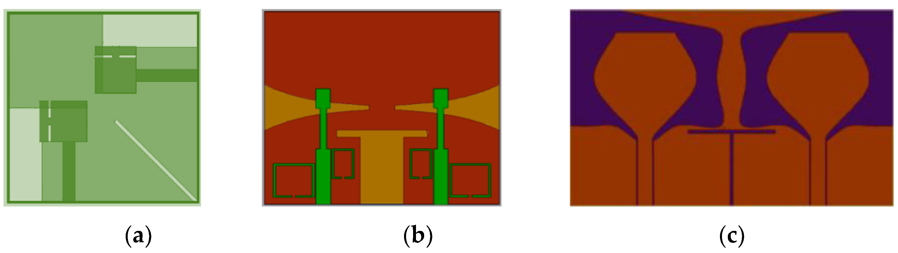
2.5. Metamaterial/Electromagnetic Band Gap (EBG) Structure
Metamaterials are artificial materials with a subwavelength feature and spatially varying geometric parameters that manipulate the phase, amplitude, and polarization of a wave [73]. A metamaterial is organized between dual electromagnetically coupled patches to remove the surface wave coupling and improve isolation. In reference [65], the AEs consisted of microstrip-fed modified circular radiators and a partial ground with stubs. A metamaterial structure was loaded around both sides of the feed line for bandwidth improvement, and mutual coupling reduction is displayed in Figure 7a. In paper [66], a four-port MIMO antenna consisted of four circular AEs with modified defected ground plane and periodic EBG structures. The EBG structures were composed of grid patterns on the top patch, as presented in Figure 7b. They were printed on the center of the dielectric substrate to lower electromagnetic coupling between the parallel elements. Additionally, by etching four crescent ring-shaped resonant slots on the radiators, a sharp band-notched characteristic was achieved. In reference [67], by loading an “EL” slot into the radiating element along with two identical stubs coupled to the partial ground, impedance matching and radiation characteristics across the band were improved, as presented in Figure 7c. To attain high port isolation, an un-protruded multi-slot (UPMS) isolating element was placed between two closely spaced AEs.
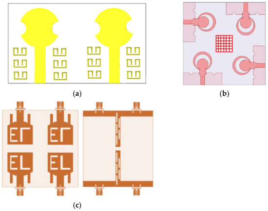
Figure 7.
Metamaterial: (a) [65], (b) [66], and (c) [67].
2.6. Parasitic Element
In this DT, a conducting structure was placed between AEs, which acts as a reflector to increase isolation. In article [68], two square-shaped radiators with W-shaped and inverted U-shaped slots on the patch were used to notch WiMAX and WLAN frequency bands, and the AEs were arranged in 90orientation to form the MIMO antenna topology, as presented in Figure 8a. A parasitic structure was embedded between two monopole antennas to enhance isolation. In paper [69], the AE was formed by a patch (square-shaped) with microstrip line feed and a defect in the ground surface, as illustrated in Figure 8b. A rectangular cut was added to the ground surface to widen the bandwidth. AEs 1 and 3 were printed on top, and AEs 2 and 4 were printed on the base of the substrate. Likewise, AEs 1 and 3 were placed orthogonally to AEs 2 and 4 to reduce mutual coupling. To further enhance isolation, two four-directional staircase-shaped patches (identical and symmetrical) were introduced in the center of the upper plane and lower plane of the MIMO antenna. In order to enhance isolation, the decoupling structure (staircase-shaped) was separated by orthogonal slots. An L-slot was added to the ground surface to reject the X-band. The HL-shaped slot was printed on the square-shaped radiator to produce a notch at the WLAN band. Also, a U-slot was introduced on the ground surface to reject the WiMAX band. In reference [70], the AEs were developed from a modified rectangular patch, and a decoupling network was designed on the lower side of the substrate to achieve high isolation, as shown in Figure 8c. A dumbbell-shaped stub is also added to the partial ground surface to suppress inter-element coupling.

Figure 8.
Parasitic element: (a) [68], (b) [69], and (c) [70].
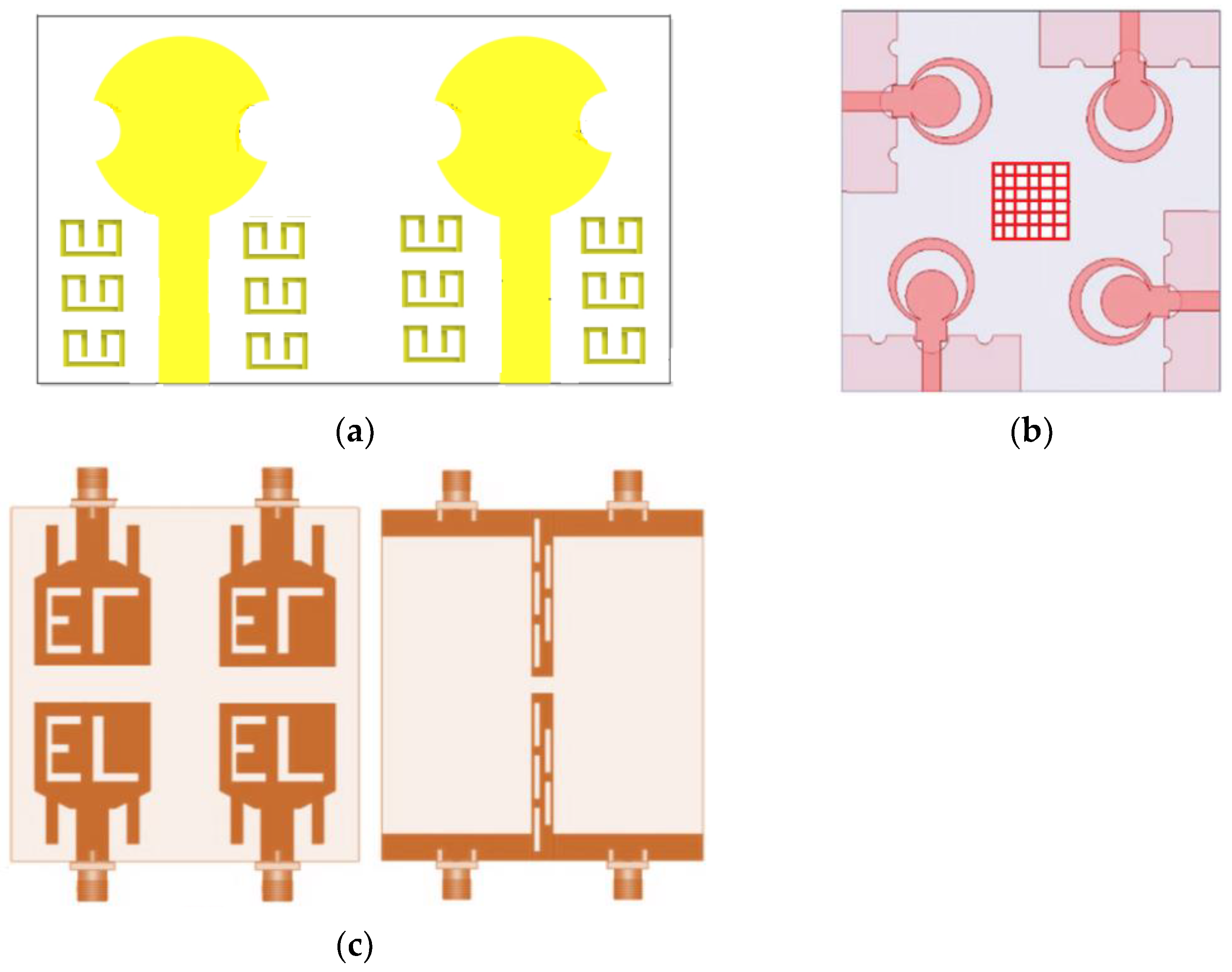
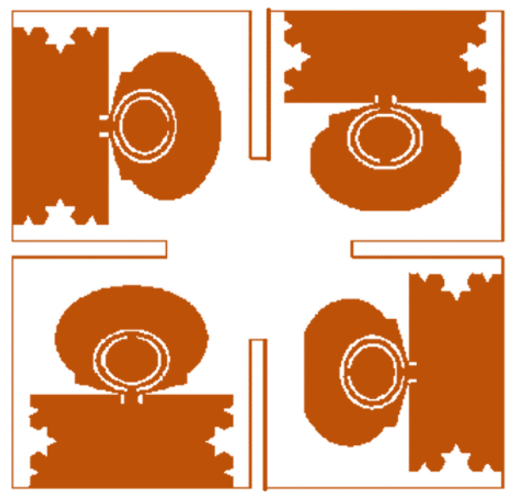
2.7. Carbon Black Film (CBF)
In this DT, the isolation among AEs is enhanced through the absorption of the electromagnetic interference between them. In article [71], disc-shaped AEs with microstrip feedings and a partial ground plane were designed, presented in Figure 9. The conduction material used was carbon black. A paste of the epoxy and carbon black was coated on the feedline of the MIMO antenna. The coated position and area were two important parameters to determine the isolation efficiency and gain of the antenna.
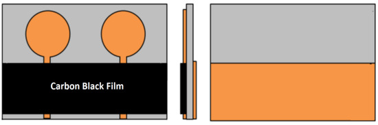
Figure 9.
Carbon black film [71].
2.8. Slotted Edge Substrate (SES)
In this DT, an open-end slot is cut from the substrate to improve isolation. In reference [72], the monopole AE consisted of an elliptical patch radiator, which is fed by a microstrip feed line, and second-order Koch fractal geometry was designed on the opposite edges of the ground, as shown in Figure 10. An elliptical CSRR was etched from the radiator to achieve two notched bands within the UWB range. Also, a U-shaped slot was added in the ground plane to obtain an improved matching within the UWB. A tapered conducting patch was placed between the elliptical patch and the feed line to maintain the full UWB frequency range. A slotted edge substrate was used to increase inter-element isolation. Table 2 presents an investigation of the literature review of various DTs.
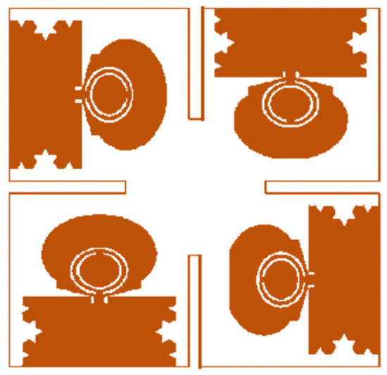
Figure 10.
Slotted edge substrate [72].
Table 2.
Summarized literature survey investigation of various DTs.
As presented in Table 2, the 180placement of AEs required a large substrate area, and metamaterial DT needed less chip area. Also, DTs such as orthogonal placement of AEs, DS, metamaterial, and CBF provided a high value of gain. Nearly all UWB MIMO antennas were printed on FR4 substrate, except a few antennas [43,44,45,63]. As compared to the orthogonal position, the 180 position of AEs provides high isolation. Among the various DTs, NL, PE, and SES provided high isolation because, in these DTs, there was no direct connection between the ground planes of AEs. Mostly, DTs that placed AEs orthogonally, DS, DGS, metamaterial, and PE were integrated into the UMAs.
3. Simulated Study of Different Decoupling Techniques
A microstrip-fed circular patch and a partial ground with an open-end slot were used as a single UWB AE for simulation [74]. The isolation between the two-port UMA (designed using the same AEs) is enhanced through the application of various DTs. The simulations were carried out using the Ansys HFSS software. The results, such as S11, S12 (mutual coupling), and 3D radiation plots, were considered for the investigation of DTs.
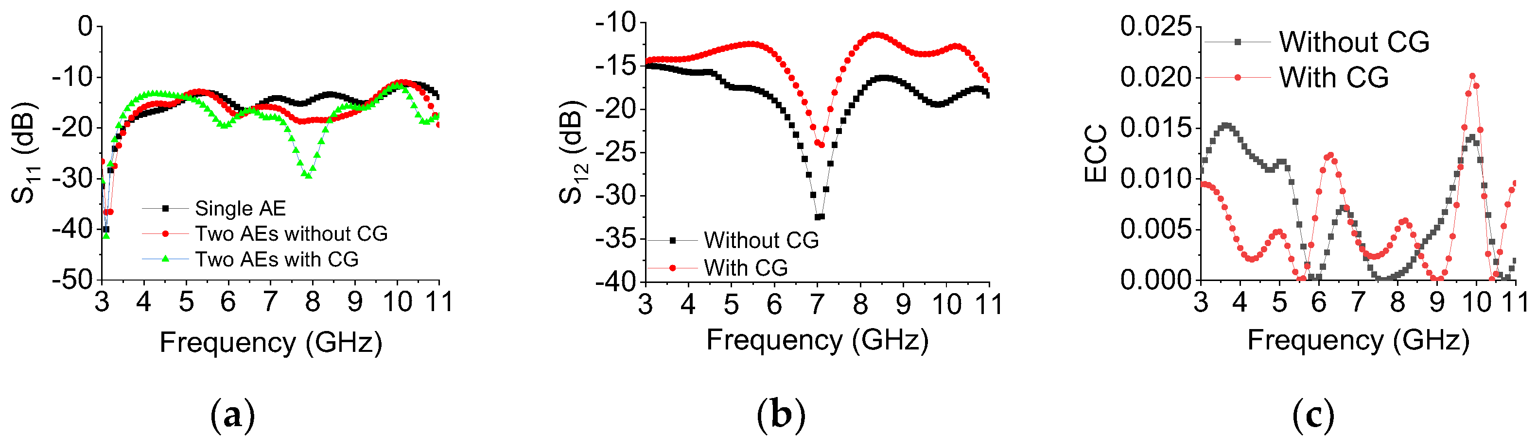
To verify the effect of mutual coupling on antenna radiation patterns, the radiation pattern/s of a single UWB AE and two-port UMA with and without CG are plotted, which are placed at quarter-wavelength separation in Figure 11. A CG design is essential for the MIMO antenna as all signal levels inside it can be measured accurately on a similar reference level. If separate and non-associated ground planes are used, the MIMO antennas may not work in real-world applications because the assumption that all ground surfaces have similar voltage levels becomes invalid [59]. The radiation pattern of a single UWB AE has an omnidirectional shape, and two-port UMAs tend to radiate in opposite directions (making the patterns orthogonal to each other) due to the mutual coupling, despite being with/without CG. This proves that the mutual coupling changes the shape of the radiation pattern.
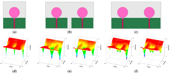
Figure 11.
(a) Isolated UWB AE, (b) two-port UMA without CG, (c) two-port UMA with CG, (d) radiation pattern of the isolated UWB AE, (e) radiation patterns of the two-port UMA without CG when port-1 and port-2 are excited separately, and (f) radiation patterns of the two-port UMA with CG when port-1 and port-2 are excited separately.
In Figure 12a, the S11 values of a single AE and a two-port UMA with/without CG are shown. As per the plot, there is not much variation in the S11 values because of the same AE/s design. In Figure 12b,c, S12 (representing mutual coupling) and ECC of two-port UMA with/without CG are displayed, respectively. The isolation without CG is higher than with CG as there is no connection between the ground planes of the two AEs, and no current will flow to the other port. Similarly, ECC values without CG are lower than those with CG. The recommended value of ECC is 0.5 for a good diversity performance of a MIMO system. It is shown in the plot that by only placing AEs with a proper gap, the ECC value is less than 0.02.
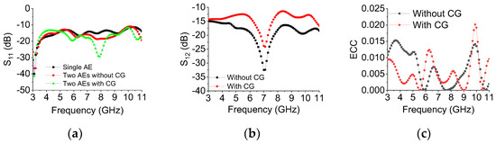
Figure 12.
(a) S11, (b) S12, and (c) ECC.
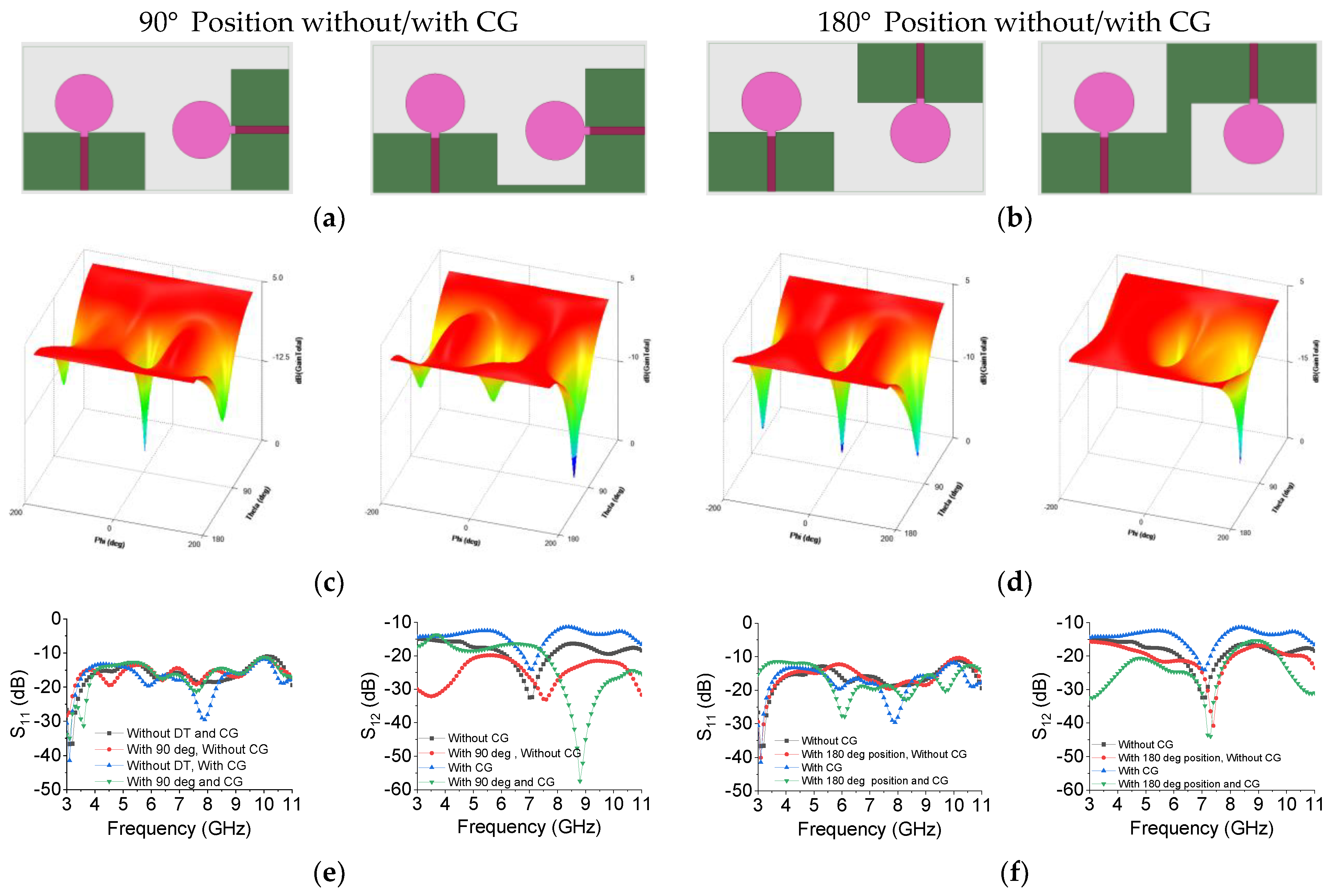
3.1. Placing AEs at 90 and 180
In Figure 13, S11, S12, and radiation patterns of the antenna configuration are shown for 90 and 180 placed AEs without/with CG. The radiation patterns of all MIMO antennas are almost the same, but the MIMO antenna with CG has some change in pattern shape. The S11 plot of all MIMO antennas is almost identical. With CG structure, isolation is very low in 90 placed AEs and very high in 180 placed AEs at lower frequencies of the UWB as the distance between different ports is higher in 180 placed AEs as compared to the 90 placed AEs. Table 3 compares the isolation results of two-port UMAs with AEs placed 90 and 180 opposite to each other.
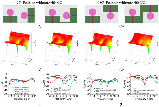
Figure 13.
(a) AEs positioned 90 without/with CG, (b) AEs positioned 180 without/with CG, (c) radiation patterns of 90 placed AEs, (d) radiation patterns of 180 placed AEs, (e) S11/S12 of 90 placed AEs, and (f) S11/S12 of 180 placed AEs.
Table 3.
Isolation results of 90 and 180° placed AEs.
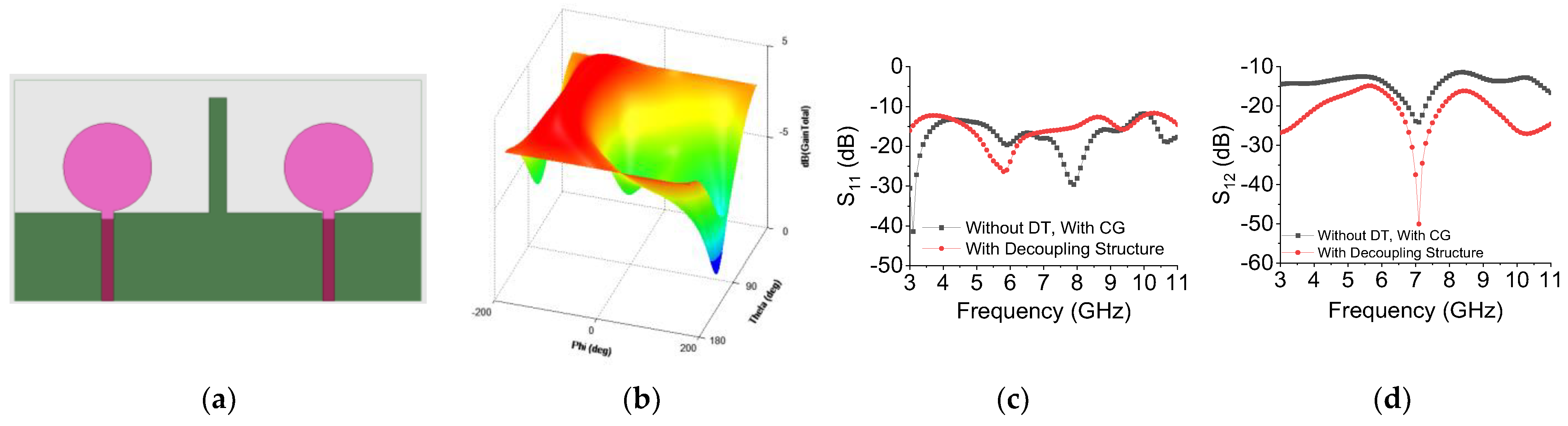
3.2. Decoupling Structure (DS)
To apply this DT, a vertical strip is added to the CG to increase isolation between two AEs. As shown in Figure 14, the radiation pattern becomes directional, and a complete UWB range is achieved. When comparing the isolation of the two-port UMA with DS to that of the antenna without DS, isolation is highly increased at the lower, middle, and higher frequency ranges.
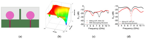
Figure 14.
(a) UMA with DS, (b) radiation pattern, (c) S11, and (d) S12.
3.3. Neutralization Line (NL)
In this DT, a ring-shaped element is connected to two L-shaped structures, which are attached to the two circular radiators shown in Figure 15. The shape of the radiation pattern becomes deformed and directional. Also, impedance matching is disturbed at lower and higher frequency ranges. The isolation of this antenna is slightly higher than two-port UMA with CG, but poor isolation is obtained at lower frequencies.
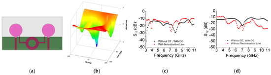
Figure 15.
(a) UMA with NL, (b) radiation pattern, (c) S11, and (d) S12.
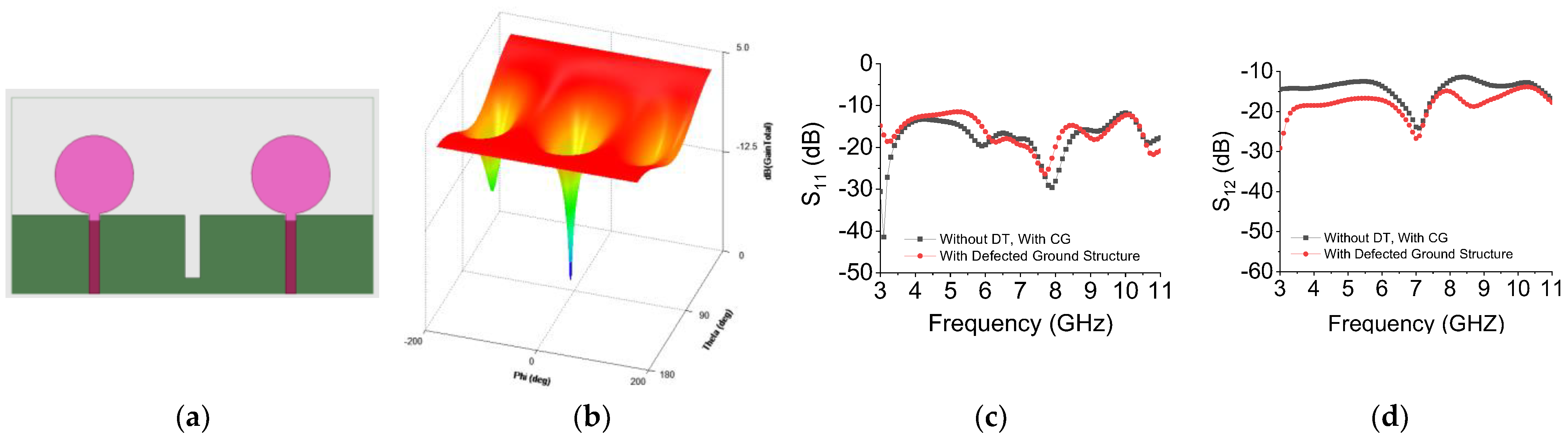
3.4. Defected Ground Structure (DGS)
A narrow vertical slot at the center of the ground plane is added to enhance isolation, as displayed in Figure 16. This antenna is almost omnidirectional and has almost the same S11 plot as two-port UMA with CG. The isolation is mainly increased at lower and higher frequency ranges as compared to two-port UMA with CG.

Figure 16.
(a) UMA with DGS, (b) radiation pattern, (c) S11, and (d) S12.
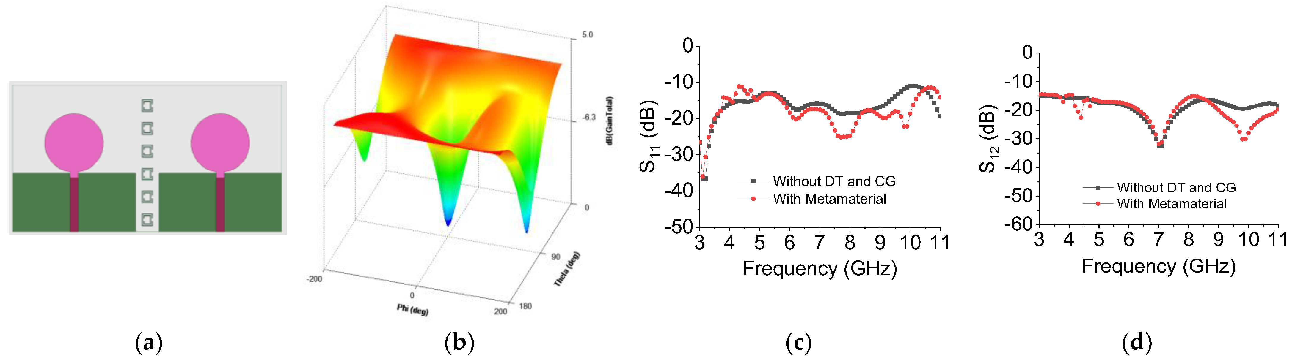
3.5. Metamaterial
In this DT, six SRR-based elements are placed vertically between antenna resonators, as shown in Figure 17.

Figure 17.
(a) UMA with metamaterial, (b) Radiation pattern, (c) S11, and (d) S12.
The shape of the radiation pattern is slightly deformed but omnidirectional. The complete UWB range is obtained with little variation at a higher frequency when compared to two-port UMA with CG. There is no change in isolation at lower and mid-frequency ranges, except in the high-frequency range.
3.6. Parasitic Element (PE)
In this DT, a narrow strip is added in the middle of the AEs at the bottom of the substrate, as shown in Figure 18. This DT makes the radiation pattern directional, and good impedance bandwidth is achieved from 3 GHz to 11 GHz. The isolation is greatly improved at lower and higher frequency bands.
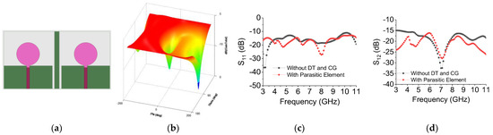
Figure 18.
(a) UMA with PE, (b) radiation pattern, (c) S11, and (d) S12.
3.7. Carbon Black Film (CBF)
In this DT, a conducting rectangular structure is designed in the middle of the feedlines, as demonstrated in Figure 19. Due to this, the shape of the radiation pattern is deformed. A bandwidth of more than 3 GHz to 11 GHz is achieved. There is a huge increase in the isolation as compared to two-port UMA with CG. The isolation varies from 30 dB to 60 dB.
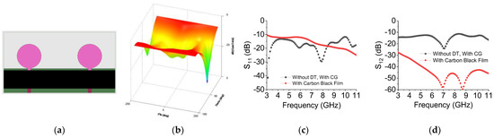
Figure 19.
(a) UMA with CBF, (b) radiation pattern, (c) S11, and (d) S12.
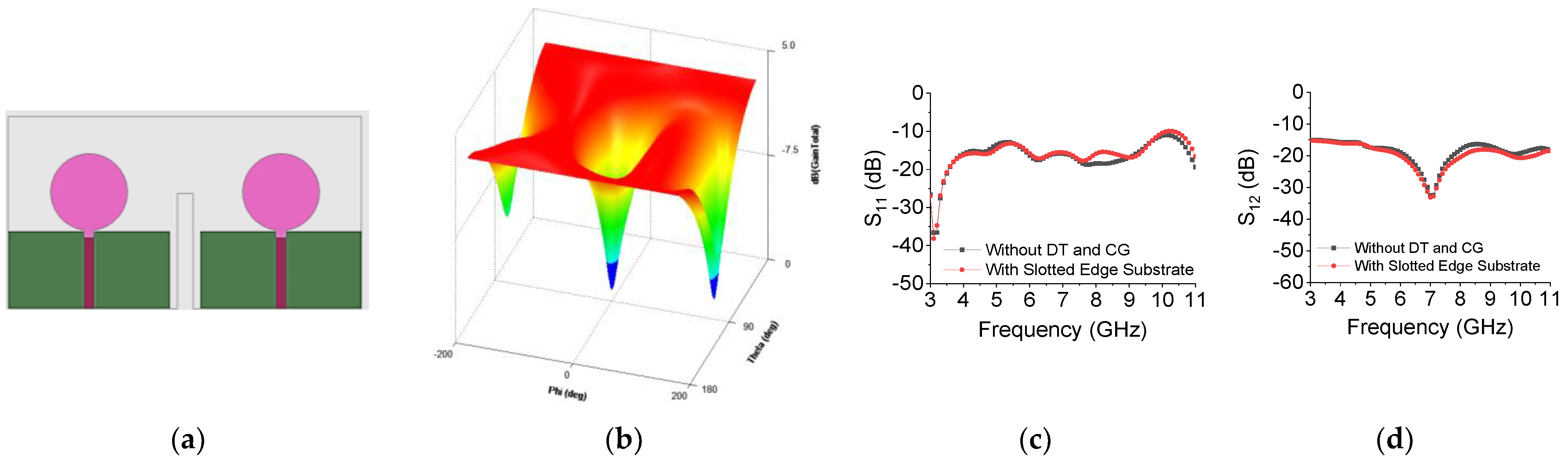
3.8. Slotted Edge Substrate (SES)
In this DT, a narrow slot is cut from the substrate to enhance isolation, as displayed in Figure 20. The radiation pattern of this antenna is almost omnidirectional. This antenna has the same S11 and S12 plots as compared to two-port UMA with CG, which shows that there is almost no change in the results of SES.

Figure 20.
(a) UMA with SES, (b) radiation pattern, (c) S11, and (d) S12.
A comparative analysis of different DTs is shown in Table 4, which is based on the simulated study and literature survey.
Table 4.
Comparative analysis of various DTs.
4. Conclusions
In this review and simulated study paper, we demonstrated how isolation is affected with and without the application of different DTs in UMAs. The mutual coupling can modify the impedance matching, reflection coefficients, and far-field radiation patterns of the AEs. Practically, the mutual coupling relies on the MIMO design as well as on the excitations of other nearby AEs. The antenna radiation pattern of a single UWB AE has an omnidirectional shape, and two-port UMAs tend to radiate in opposite directions (making the patterns orthogonal to each other) due to the mutual coupling, with/without CG. The isolation without CG is higher than with CG because, due to the lack of connection between the ground planes of both AEs, no current will flow to the other port. Similarly, the ECC of the antenna without CG is lower than that with CG. By maintaining a proper gap between AEs, an ECC of less than 0.02 is achieved. The MIMO antenna with CG causes changes in the shape of the radiation pattern. The isolation is greater in 90 placed AEs as compared to 180 placed AEs. With CG structure, isolation is very low in 90 placed AEs and very high in 180 placed AEs at lower frequencies of the UWB. In DS, the radiation pattern becomes directional. With two-port UMA with CG, isolation is highly increased at the lower, middle, and higher frequency ranges. In NL, the shape of the radiation pattern is deformed and becomes directional. Also, impedance matching is disturbed at lower and higher frequency ranges, and poor isolation is obtained at lower frequencies. In DGS, an almost omnidirectional radiation pattern is obtained, and the isolation is mainly increased at lower and higher frequency ranges as compared to two-port UMA with CG. In metamaterial DT, the shape of the radiation pattern is slightly deformed but omnidirectional. There is no change in the isolation at lower and mid-frequency ranges, except in the high-frequency range in contrast with two-port UMA without CG. In PE, the directional radiation pattern and good impedance bandwidth are achieved in the UWB range. The isolation is greatly improved at lower and higher frequency bands. In CBF, the shape of the radiation pattern is deformed. There is a huge increase in the isolation as compared to two-port UMA with CG. In SES, an almost omnidirectional radiation pattern is obtained as compared to two-port UMA with CG, where there is almost no change in the isolation.
Each DT has its own benefits and limitations. However, as per the literature survey, placing AEs at a 180 orientation, NL, PE, and SES provide high isolation because, in these DTs, there is no direct connection between the ground planes of AE. Based on the simulated study, CBF and placing AEs at a 180 orientation provides high isolation even if the ground is connected. However, when the ground is not connected, placing AEs at a 90 orientation provides high isolation. This review article will help future works in many ways. Using the literature survey, one can understand the issues of recently reported work on DTs. Using the simulated study, researchers can estimate the effect of applying various DTs on various parameters, such as impedance matching, isolation, and pattern. The proposed review articles can save researchers time when selecting an appropriate DT without compromising the antenna performance.
Author Contributions
Conceptualization, S.J., G.S. and S.K.; formal analysis, S.J., H.M. and H.C.C.; investigation, B.G., H.C.C. and K.W.K.; writing—original draft preparation, S.J.; writing—review and editing, S.K. and K.W.K.; supervision, G.S. All authors have read and agreed to the published version of the manuscript.
Funding
Princess Nourah bint Abdulrahman University Researchers Supporting Project number (PNURSP2023R137), Princess Nourah bint Abdulrahman University, Riyadh, Saudi Arabia.
Data Availability Statement
Not applicable.
Acknowledgments
This research was supported in part by the National Research and Development Program through the National Research Foundation of Korea (NRF) funded by the Ministry of Education (No. NRF-2022R1I1A3064460) and in part by the BK21 FOUR project funded by the Ministry of Education (No. 4199990113966).
Conflicts of Interest
The authors declare no conflict of interest.
References
- Zhang, R.; Liang, Y.C.; Hall PS, P.; Gardner, P.; Kelly, J.; Ebrahimi, E. Federal Communications Commission Revision of Part 15 of the Commission’s Rules Regarding Ultra-Wideband Transmission System from 3.1 to 10.6 GHz; ET-Docket; Federal Communications Commission: Washington, DC, USA, 2002; pp. 98–153. [Google Scholar]
- Jiang, S.; Zhao, C.; Zhu, Y.; Wang, C.; Du, Y. A Practical and Economical Ultra-wideband Base Station Placement Approach for Indoor Autonomous Driving Systems. J. Adv. Transp. 2022, 2022, 3815306. [Google Scholar] [CrossRef]
- Saad, A.A.R.; Mohamed, H.A. Conceptual design of a compact four-element UWB MIMO slot antenna array. IET Microw. Antennas Propag. 2019, 13, 208–215. [Google Scholar] [CrossRef]
- Wilhite, T. Uses of Ultrawide Band Antennas. Turbo Future. 2 February 2021. Available online: https://turbofuture.com/industrial/Uses-of-Ultrawide-Band-Antennas (accessed on 1 March 2023).
- Zhu, F.; Gao, S.; Ho, A.T.; Abd-Alhameed, R.A.; See, C.H.; Brown, T.W.C.; Li, J.; Wei, G.; Xu, J. Multiple Band-Notched UWB Antenna with Band-Rejected Elements Integrated in the Feed Line. IEEE Trans. Antennas Propag. 2013, 61, 3952–3960. [Google Scholar] [CrossRef]
- Foschini, G.J. Layered space-time architecture for wireless communication in a fading environment when using multi-element antennas. Bell Labs Tech. J. 2002, 1, 41–59. [Google Scholar] [CrossRef]
- Paulraj, A.; Gore, D.; Nabar, R.; Bolcskei, H. An Overview of MIMO Communications—A Key to Gigabit Wireless. Proc. IEEE 2004, 92, 198–218. [Google Scholar] [CrossRef]
- Zhang, C.; Xiao, P.; Zhao, Z.-T.; Liu, Z.; Yu, J.; Hu, X.-Y.; Chu, H.-B.; Xu, J.-J.; Liu, M.-Y.; Zou, Q.; et al. A Wearable Localized Surface Plasmons Antenna Sensor for Communication and Sweat Sensing. IEEE Sens. J. 2023, 23, 11591–11599. [Google Scholar] [CrossRef]
- Yao, Y.; Shu, F.; Li, Z.; Cheng, X.; Wu, L. Secure Transmission Scheme Based on Joint Radar and Communication in Mobile Vehicular Networks. IEEE Trans. Intell. Transp. Syst. 2023, 24, 10027–10037. [Google Scholar] [CrossRef]
- Lin, Z.; Lin, M.; Champagne, B.; Zhu, W.-P.; Al-Dhahir, N. Secrecy-Energy Efficient Hybrid Beamforming for Satellite-Terrestrial Integrated Networks. IEEE Trans. Commun. 2021, 69, 6345–6360. [Google Scholar] [CrossRef]
- Lin, Z.; Niu, H.; An, K.; Wang, Y.; Zheng, G.; Chatzinotas, S.; Hu, Y. Refracting RIS-Aided Hybrid Satellite-Terrestrial Relay Networks: Joint Beamforming Design and Optimization. IEEE Trans. Aerosp. Electron. Syst. 2022, 58, 3717–3724. [Google Scholar] [CrossRef]
- Lin, Z.; An, K.; Niu, H.; Hu, Y.; Chatzinotas, S.; Zheng, G.; Wang, J. SLNR-based Secure Energy Efficient Beamforming in Multibeam Satellite Systems. IEEE Trans. Aerosp. Electron. Syst. 2022, 59, 2085–2088. [Google Scholar] [CrossRef]
- An, K.; Lin, M.; Ouyang, J.; Zhu, W.P. Secure Transmission in Cognitive Satellite Terrestrial Networks. IEEE J. Sel. Areas Commun. 2016, 34, 3025–3037. [Google Scholar] [CrossRef]
- Li, A.; Masouros, C.; Vucetic, B.; Li, Y.; Swindlehurst, A.L. Interference Exploitation Precoding for Multi-Level Modulations: Closed-Form Solutions. IEEE Trans. Commun. 2020, 69, 291–308. [Google Scholar] [CrossRef]
- Pan, S.; Lin, M.; Xu, M.; Zhu, S.; Bian, L.A.; Li, G. A Low-Profile Programmable Beam Scanning Holographic Array Antenna without Phase Shifters. IEEE Internet Things J. 2021, 9, 8838–8851. [Google Scholar] [CrossRef]
- Li, B.; Zhang, M.; Rong, Y.; Han, Z. Transceiver Optimization for Wireless Powered Time-Division Duplex MU-MIMO Systems: Non-Robust and Robust Designs. IEEE Trans. Wirel. Commun. 2021, 21, 4594–4607. [Google Scholar] [CrossRef]
- Chen, Z.; Tang, J.; Zhang, X.Y.; So, D.K.C.; Jin, S.; Wong, K.-K. Hybrid Evolutionary-Based Sparse Channel Estimation for IRS-Assisted mmWave MIMO Systems. IEEE Trans. Wirel. Commun. 2021, 21, 1586–1601. [Google Scholar] [CrossRef]
- Li, A.; Masouros, C.; Swindlehurst, A.L.; Yu, W. 1-Bit Massive MIMO Transmission: Embracing Interference with Symbol-Level Precoding. IEEE Commun. Mag. 2021, 59, 121–127. [Google Scholar] [CrossRef]
- Feng, Y.; Zhang, B.; Liu, Y.; Niu, Z.; Fan, Y.; Chen, X. A D-Band Manifold Triplexer with High Isolation Utilizing Novel Waveguide Dual-Mode Filters. IEEE Trans. Terahertz Sci. Technol. 2022, 12, 678–681. [Google Scholar] [CrossRef]
- Liu, Y.; Xu, K.-D. Millimeter-Wave Bandpass Filters Using On-Chip Dual-Mode Resonators in 0.13-μm SiGe BiCMOS Technology. IEEE Trans. Microw. Theory Tech. 2023, 71, 3650–3660. [Google Scholar] [CrossRef]
- Xu, K.-D.; Liu, Y. Millimeter-Wave On-Chip Bandpass Filter Using Complementary-Broadside-Coupled Structure. IEEE Trans. Circuits Syst. II Express Briefs 2023, 70, 2829–2833. [Google Scholar] [CrossRef]
- Xu, K.-D.; Guo, Y.-J.; Liu, Y.; Deng, X.; Chen, Q.; Ma, Z. 60-GHz Compact Dual-Mode On-Chip Bandpass Filter Using GaAs Technology. IEEE Electron. Device Lett. 2021, 42, 1120–1123. [Google Scholar] [CrossRef]
- Dai, B.; Zhang, B.; Niu, Z.; Feng, Y.; Liu, Y.; Fan, Y. A Novel Ultrawideband Branch Waveguide Coupler with Low Amplitude Imbalance. IEEE Trans. Microw. Theory Tech. 2022, 70, 3838–3846. [Google Scholar] [CrossRef]
- Huang, X.; Zhou, L.; Xu, J.-X.; Zhang, X.Y.; Mao, J.-F. BCB-Based Thin-Film Ka-Band Quarter-Mode SIW Packaged Filters with Ultrawide Stopband and Independently Controlled TZs. IEEE Trans. Microw. Theory Tech. 2022, 70, 4389–4398. [Google Scholar] [CrossRef]
- Huang, X.-L.; Zhou, L.; Yuan, Y.; Qiu, L.-F.; Mao, J.-F. Quintuple-Mode W-Band Packaged Filter Based on a Modified Quarter-Mode Substrate-Integrated Waveguide Cavity. IEEE Trans. Compon. Packag. Manuf. Technol. 2019, 9, 2237–2247. [Google Scholar] [CrossRef]
- Allen, J.L.; Diamond, B.L. Mutual Coupling in Array Antennas; MIT Lincoln Laboratory: Lexington, MA, USA, 1966. [Google Scholar] [CrossRef]
- Ding, G.; Anselmi, N.; Xu, W.; Li, P.; Rocca, P. Interval-Bounded Optimal Power Pattern Synthesis of Array Antenna Excitations Robust to Mutual Coupling. IEEE Antennas Wirel. Propag. Lett. 2023, 1–5. [Google Scholar] [CrossRef]
- Chung, K.L.; Tian, H.; Wang, S.; Feng, B.; Lai, G. Miniaturization of microwave planar circuits using composite microstrip/coplanar-waveguide transmission lines. Alex. Eng. J. 2022, 61, 8933–8942. [Google Scholar] [CrossRef]
- Kaiser, T.; Zheng, F.; Dimitrov, E. An Overview of Ultra-Wide-Band Systems with MIMO. Proc. IEEE 2009, 97, 285–312. [Google Scholar] [CrossRef]
- Cherry, S. Edholm’s Law of Bandwidth. IEEE Spectr. 2004, 41, 58–60. [Google Scholar] [CrossRef]
- Saritha, V.; Chandrasekhar, C. A Study and Review on Frequency Band Notch Characteristics in Reconfgurable MIMO UWB Antennas. Wirel. Pers. Commun. 2021, 118, 2631–2661. [Google Scholar] [CrossRef]
- Jhunjhunwala, V.K.; Ali, T.; Kumar, P.; Kumar, P.; Kumar, P.; Shrivastava, S.; Bhagwat, A.A. Flexible UWB and MIMO Antennas for Wireless Body Area Network: A Review. Sensors 2022, 22, 9549. [Google Scholar] [CrossRef]
- Gnanaharan, I.; Anbazhagan, R. Review on the Design of the Isolation Techniques for UWB-MIMO Antennas. Adv. Electromagn. 2018, 7, 46–70. [Google Scholar] [CrossRef]
- Sheriff, N.; Rahim, S.K.A.; Chattha, H.T.; Geok, T.K. Multiport Single Element Mimo Antenna Systems: A Review. Sensors 2023, 23, 747. [Google Scholar] [CrossRef]
- Yadav, R.; Malviya, L. UWB antenna and MIMO antennas with bandwidth, band-notched, and isolation properties for high-speed data rate wireless communication: A review. Int. J. RF Microw. Comput.-Aided Eng. 2019, 30, e22033. [Google Scholar] [CrossRef]
- Srividhya, K.; Habiba, H.U. MIMO Antennas—A review. Int. J. Res. Anal. Rev. 2019, 6, 179–186. [Google Scholar]
- Naser, S.; Dib, N. A Compact Printed UWB Pacman-Shaped MIMO Antenna with Two Frequency Rejection Bands. Jordanian J. Comput. Inf. Technol. 2016, 2, 1–6. [Google Scholar] [CrossRef]
- Toktas, A.; Akdagli, A. Compact multiple-input multiple-output antenna with low correlation for ultra-wide wideband. IET Microw. Antennas Propag. 2015, 9, 822–829. [Google Scholar] [CrossRef]
- Srivastava, K.; Kumar, A.; Kanaujia, B.K.; Dwari, S.; Kumar, S. A CPW-fed UWB MIMO antenna with integrated GSM band and dual band notches. Int. J. RF Microw. Comput. Eng. 2018, 29, e21433. [Google Scholar] [CrossRef]
- Sultan, K.S.; Abdullah, H.H. Planar Uwb Mimo-Diversity Antenna with Dual Notch Characteristics. Prog. Electromagn. Res. C 2019, 93, 119–129. [Google Scholar] [CrossRef]
- Naktong, W.; Ruengwaree, A. Four-Port Rectangular Monopole Antenna for Uwb-Mimo Applications. Prog. Electromagn. Res. B 2020, 87, 19–38. [Google Scholar] [CrossRef]
- Mathur, R.; Dwari, S. Compact 4-Port MIMO/Diversity Antenna with Low Correlation for UWB Application. Frequenz 2018, 72, 429–435. [Google Scholar] [CrossRef]
- Arumugam, S.; Manoharan, S.; Palaniswamy, S.K.; Kumar, S. Design and Performance Analysis of a Compact Quad-Element UWB MIMO Antenna for Automotive Communications. Electronics 2021, 10, 2184. [Google Scholar] [CrossRef]
- Govindan, T.; Palaniswamy, S.K.; Kanagasabai, M.; Kumar, S. Design and Analysis of UWB MIMO Antenna for Smart Fabric Communications. Int. J. Antennas Propag. 2022, 2022, 5307430. [Google Scholar] [CrossRef]
- Jayant, S.; Srivastava, G.; Kumar, S. Quad-Port UWB MIMO Footwear Antenna for Wearable Applications. IEEE Trans. Antennas Propag. 2022, 70, 7905–7913. [Google Scholar] [CrossRef]
- Raheja, D.K.; Kumar, S.; Kanaujia, B.K. Compact quasi-elliptical-self-complementary four-port super-wideband MIMO antenna with dual band elimination characteristics. AEU-Int. J. Electron. Commun. 2019, 114, 153001. [Google Scholar] [CrossRef]
- Naser, S.; Dib, N. Analysis and Design of MIMO Antenna for UWB Applications Based on The Super-Formula. In Proceedings of the 2016 5th International Conference on Electronic Devices, Systems and Applications (ICEDSA), Ras Al Khaimah, United Arab Emirates, 6–8 December 2016. [Google Scholar]
- Wu, Y.; Ding, K.; Zhang, B.; Li, J.; Wu, D.; Wang, K. Design of a Compact UWB MIMO Antenna without Decoupling Structure. Int. J. Antennas Propag. 2018, 2018, 9685029. [Google Scholar] [CrossRef]
- Jayant, S.; Srivastava, G.; Kumar, S. Pattern diversity and isolation enhancement of UWB MIMO antenna based on characteristic modes for mobile terminals. Int. J. Microw. Wirel. Technol. 2022, 15, 793–804. [Google Scholar] [CrossRef]
- Chacko, B.P.; Augustin, G.; Denidni, T.A. Uniplanar polarisation diversity antenna for ultrawideband systems. IET Microw. Antennas Propag. 2013, 7, 851–857. [Google Scholar] [CrossRef]
- Gao, P.; He, S.; Wei, X.; Xu, Z.; Wang, N.; Zheng, Y. Compact Printed UWB Diversity Slot Antenna with 5.5-GHz Band-Notched Characteristics. IEEE Antennas Wirel. Propag. Lett. 2014, 13, 376–379. [Google Scholar] [CrossRef]
- Zhu, J.; Li, S.; Feng, B.; Deng, L.; Yin, S. Compact Dual-Polarized UWB Quasi-Self-Complementary MIMO/Diversity Antenna with Band-Rejection Capability. IEEE Antennas Wirel. Propag. Lett. 2015, 15, 905–908. [Google Scholar] [CrossRef]
- Jetti, C.R.; Nandanavanam, V.R. Compact Mimo Antenna with Wlan Band-Notch Characteristics For Portable Uwb Systems. Prog. Electromagn. Res. C 2018, 88, 1–12. [Google Scholar] [CrossRef]
- Chandel, R.; Gautam, A. Compact MIMO/diversity slot antenna for UWB applications with band-notched characteristic. Electron. Lett. 2016, 52, 336–338. [Google Scholar] [CrossRef]
- Addepalli, T.; Desai, A.; Elfergani, I.; Anveshkumar, N.; Kulkarni, J.; Zebiri, C.; Rodriguez, J.; Abd-Alhameed, R. 8-Port Semi-Circular Arc MIMO Antenna with an Inverted L-Strip Loaded Connected Ground for UWB Applications. Electronics 2021, 10, 1476. [Google Scholar] [CrossRef]
- Ali, W.A.; Ibrahim, A.A. A compact double-sided MIMO antenna with an improved isolation for UWB applications. AEU-Int. J. Electron. Commun. 2017, 82, 7–13. [Google Scholar] [CrossRef]
- Jayant, S.; Srivastava, G. Close-Packed Quad-Element Triple-Band-Notched UWB MIMO Antenna with Upgrading Capability. IEEE Trans. Antennas Propag. 2022, 71, 353–360. [Google Scholar] [CrossRef]
- Kumar, S.; Lee, G.H.; Kim, D.H.; Mohyuddin, W.; Choi, H.C.; Kim, K.W. Multiple-input-multiple-output/diversity antenna with dual band-notched characteristics for ultra-wideband applications. Microw. Opt. Technol. Lett. 2019, 62, 336–345. [Google Scholar] [CrossRef]
- Kumar, S.; Lee, G.H.; Kim, D.H.; Mohyuddin, W.; Choi, H.C.; Kim, K.W. A compact four-port UWB MIMO antenna with connected ground and wide axial ratio bandwidth. Int. J. Microw. Wirel. Technol. 2019, 12, 75–85. [Google Scholar] [CrossRef]
- Tiwari, R.N.; Singh, P.; Kanaujia, B.K.; Srivastava, K. Neutralization technique based two and four port high isolation MIMO antennas for UWB communication. AEU-Int. J. Electron. Commun. 2019, 110, 152828. [Google Scholar] [CrossRef]
- Zhang, S.; Pedersen, G.F. Mutual Coupling Reduction for UWB MIMO Antennas with a Wideband Neutralization Line. IEEE Antennas Wirel. Propag. Lett. 2015, 15, 166–169. [Google Scholar] [CrossRef]
- Ren, J.; Hu, W.; Yin, Y.; Fan, R. Compact Printed MIMO Antenna for UWB Applications. IEEE Antennas Wirel. Propag. Lett. 2014, 13, 1517–1520. [Google Scholar] [CrossRef]
- Li, Z.; Yin, C.; Zhu, X. Compact UWB MIMO Vivaldi Antenna with Dual Band-Notched Characteristics. IEEE Access 2019, 7, 38696–38701. [Google Scholar] [CrossRef]
- Jansari, D.V.; Amineh, R.K. A two-element antenna array for compact portable MIMO-UWB communication systems. AIMS Electron. Electr. Eng. 2019, 3, 224–232. [Google Scholar] [CrossRef]
- Jabire, A.H.; Ghaffar, A.; Li, X.J.; Abdu, A.; Saminu, S.; Alibakhshikenari, M.; Falcone, F.; Limiti, E. Metamaterial Based Design of Compact UWB/MIMO Monopoles Antenna with Characteristic Mode Analysis. Appl. Sci. 2021, 11, 1542. [Google Scholar] [CrossRef]
- Wu, W.; Yuan, B.; Wu, A. A Quad-Element UWB-MIMO Antenna with Band-Notch and Reduced Mutual Coupling Based on EBG Structures. Int. J. Antennas Propag. 2018, 2018, 8490740. [Google Scholar] [CrossRef]
- Kulkarni, J.; Desai, A.; Sim, C.-Y.D. Wideband Four-Port MIMO antenna array with high isolation for future wireless systems. AEU-Int. J. Electron. Commun. 2020, 128, 153507. [Google Scholar] [CrossRef]
- Azarm, B.; Nourinia, J.; Ghobadi, C.; Majidzadeh, M. Highly isolated dual band stop two-element UWB MIMO antenna topology for wireless communication applications. J. Instrum. 2019, 14, P10036. [Google Scholar] [CrossRef]
- Tang, Z.; Wu, X.; Zhan, J.; Hu, S.; Xi, Z.; Liu, Y. Compact UWB-MIMO Antenna with High Isolation and Triple Band-Notched Characteristics. IEEE Access 2019, 7, 19856–19865. [Google Scholar] [CrossRef]
- Amin, F.; Saleem, R.; Shabbir, T.; Rehman, S.U.; Bilal, M.; Shafique, M.F. A Compact Quad-Element UWB-MIMO Antenna System with Parasitic Decoupling Mechanism. Appl. Sci. 2019, 9, 2371. [Google Scholar] [CrossRef]
- Lin, G.-S.; Sung, C.-H.; Chen, J.-L.; Chen, L.-S.; Houng, M.-P. Isolation Improvement in UWB MIMO Antenna System Using Carbon Black Film. IEEE Antennas Wirel. Propag. Lett. 2016, 16, 222–225. [Google Scholar] [CrossRef]
- Raheja, D.K.; Kanaujia, B.K.; Kumar, S. Compact four-port MIMO antenna on slotted-edge substrate with dual-band rejection characteristics. Int. J. RF Microw. Comput.-Aided Eng. 2019, 29, e21756. [Google Scholar] [CrossRef]
- Zhang, Y.; He, Y.; Wang, H.; Sun, L.; Su, Y. Ultra-Broadband Mode Size Converter Using On-Chip Metamaterial-Based Luneburg Lens. ACS Photon. 2020, 8, 202–208. [Google Scholar] [CrossRef]
- Liang, J.; Chiau, C.; Chen, X.; Parini, C. Study of a printed circular disc monopole antenna for UWB systems. IEEE Trans. Antennas Propag. 2005, 53, 3500–3504. [Google Scholar] [CrossRef]


Disclaimer/Publisher’s Note: The statements, opinions and data contained in all publications are solely those of the individual author(s) and contributor(s) and not of MDPI and/or the editor(s). MDPI and/or the editor(s) disclaim responsibility for any injury to people or property resulting from any ideas, methods, instructions or products referred to in the content. |
© 2023 by the authors. Licensee MDPI, Basel, Switzerland. This article is an open access article distributed under the terms and conditions of the Creative Commons Attribution (CC BY) license (https://creativecommons.org/licenses/by/4.0/).