Article

A Flexible Solid-State Marx Modulator Module Based on Discrete Magnetic Coupling Drivers

Department of Light Sources and Illuminating Engineering, School of Information Science and Technology, Fudan University, Shanghai 200433, China
*
Author to whom correspondence should be addressed.
Electronics 2023, 12(18), 3831; https://doi.org/10.3390/electronics12183831
Submission received: 16 August 2023 / Revised: 7 September 2023 / Accepted: 8 September 2023 / Published: 10 September 2023

Abstract

:
With the increasing and deepening application of high-voltage nanosecond solid-state pulse generators in biological, industrial, and environmental fields, the development of existing pulse generators faces many challenges, such as fixed pulse shapes, the usage of isolated driver power supplies, lower power density, and limited output electrical performance. Hence, a novel high-frequency multilevel nanosecond modular solid-state Marx modulator (SSMM) based on discrete magnetic coupling gate drivers is proposed. The gate voltage of the two MOSFETs can be rapidly synchronized at a high repetition frequency to achieve an amplitude-controlled gate voltage within 100 ns. The feasibility of the driver was verified by PSpice simulation and prototype testing. Moreover, a stackable SSMM module (S2M3) structure is proposed to solve the problem of common-mode interference conducted through the driver, which improves the reusability, scalability, and redundancy of modulators. The characteristic parameters of the developed 14-stage S2M3 are as follows: an output voltage amplitude of 5.45 kV with a 100 ns–50 ms width, a minimum rise time of approximately 18 ns, and a continuous repetition frequency of 100 kHz. S2M3 has the ability to change the pulse shape, and the pulse frequency can reach 2.8 MHz within the burst.

1. Introduction

Different applications have distinct requirements for high-voltage pulses, and conventional pulse power generators can only produce rectangular or exponential waves [1,2,3]. As semiconductor technology advances, semiconductor switches have achieved remarkable improvements in switching speed and power handling capacity, with features such as small size, long lifespan, high switching frequency, and strong controllability gradually supplanting traditional gap switches, enabling the generator to output more adjustable electrical parameters with greater flexibility. The fundamental principle of a multilevel pulse modulator is to control the on-off state of a series of power semiconductor switches by generating adjustable pulses with variable rising/falling times, a flat top, reducing the output voltage rate of change (dv/dt), and reducing peak overshoot. It can also create different waveform shapes. In fields such as low-temperature plasma, pulsed electric field sterilization, electroporation biotechnology, electrical equipment insulation testing, and other pulse power applications, research has become increasingly popular [4,5,6,7].
There are several existing types of multilevel pulse modulators, such as linear transformer drivers (LTD), solid-state pulse power modulators (SSPPM), modular multilevel converters (MMC), and SSMM. Due to the magnetic core, LTD has low efficiency, a large volume, and an output pulse width constrained by the magnetic core characteristics [8]. SSPPM suffers from poor regulation accuracy due to charging voltage imbalances caused by transformer core differences [9]. MMC has modularized redundant scalability hardware features but also obvious drawbacks. It requires a high-voltage DC power supply for capacitor series charging and voltage sensors to ensure capacitor voltage balance [10]. Compared with these generators, SSMM has its own unique advantages. Marx is a kind of electrical circuit that can produce a high-voltage pulse from a low-voltage DC input. It has two basic operation steps: storage capacitor charging in parallel and discharging in series. The main advantage of parallel charging is that it can balance the charge of each stage capacitor without using voltage sensors. Marx pulse generators have various classic circuit topologies [11]. SSMM with the modular Marx multilevel converter diode (M3CD) cells in series stacking mode [12,13,14] has active pull-down characteristics that eliminate the need for pull-down resistors to achieve low loss and high repetition frequency of the output pulse, compared with [15].
Table 1 shows the key performance characteristics of existing drivers for pulse generators.
The gate drivers of each stage operate on elevated ground during the discharge [11]. In existing multilevel pulse generators, the drivers rely on multiple optical fibers or optocouplers to transmit trigger signals, which the driver chips then amplify to drive power semiconductor switches. Commercial optocoupler drivers typically have insulation of less than 5 kV, while optical fibers offer high isolation and response speed, making them the predominant driver for current multilevel pulse generators. Each optical fiber receiver and driver chip needs an isolated DC voltage of several to tens of volts to function properly. At present, commercially isolated DC-DC [15] converters, high-frequency isolation [16] transformers diode strings [28] and air-isolation modules [29] are the main isolated power supply methods. Miniaturization is the prevailing development trend of pulse generators [30] but numerous trigger optical fibers dispersed in space and the requisite isolated power supply impair space utilization and impede system integration, and fiber optic transceivers are more expensive [9,15,17,18,19]. Although some researchers have employed a self-triggered driver in Marx generators [25,26], it has certain constraints on capacitor charging voltage, and a self-triggered driver cannot control each semiconductor switch independently, which results in a long output pulse tail and a single pulse waveform. Such as series-core magnetic coupling [20,21,22,23,24] drivers, the driving power for all switches comes from the primary winding, which is connected to the half-bridge circuit, and high-voltage coaxial cables are necessary to transmit the drive signals, ensuring insulation while shielding against electromagnetic interference. It is the most economical solution for rectangular pulse generators; however, the ability to adjust the pulse waveform is poor. Opto-magnetic driver: the use of multiple optical fibers to transmit the trigger signals to the primary winding of each pulse transformer for amplification, then the pulse transformer to transmit the drive signals and magnetic isolation of the high-voltage output [27]. In this way, the maximum pulse width of the drive signal is limited by the saturation of the transformer core. Although optical fiber can ensure the synchronization of the signals and eliminate interference from the signal and FPGA controller, the power cost and footprint will increase.
The discrete magnetic coupling driver proposed in this paper is small in size, stable in operation, requires no optical signals for pulse control, has an isolated power supply, and uses high-voltage coaxial cables. The multi-channel trigger signals emitted by the field programmable gate array (FPGA) are transferred to each discrete magnetic coupling driver through a multi-core coaxial shielding cable after level conversion and modulated into bipolar narrow pulses through an independent on/off narrow pulse circuit. The accumulation of transformer remanence and saturation of the transformer core caused by long driving pulse widths are effectively avoided. The narrow pulse and energy are then transferred to the driving circuit through the finger-sized magnetic core to restore the drive signal and control the switching of each MOSFET. The coaxial shielding cable ensures the synchronization and reliability of multi-channel trigger signals.
It is worth noting that some common-mode interference will be conducted to the low-voltage control system through the transformer during the pulse discharge process [31] and the interference level is proportional to the voltage amplitude, repetition frequency, and rising/falling time of the output pulse. Although the common-mode inductor can be added outside the coaxial shielding cable or changed in the PCB design to increase the impedance on the common-mode conduction path, it is impossible to completely cut off the conduction path, which means the low-voltage control system may not work properly when designing pulse power sources with higher output electrical parameters.
Therefore, in this paper, firstly, a S2M3 structure based on the drivers is introduced. The S2M3 has an independent power supply, a Marx circuit, drivers, a control system, optical fiber communication, and synchronous starting. Under the condition of ensuring reliable and stable operation of one module, when several lower voltage modules are serially stacked to generate a higher voltage, the maximum voltage endured by each driver in each module and its common-mode interference intensity to the control system remain constant. In addition, the voltage and current pulse parameters can be expanded flexibly with only a few optical fibers and cable connections when stacked with multiple modules, eliminating the need for additional hardware circuits. The structure can not only enhance the output electrical parameter capability of SSMM but also improve its reusability, scalability, and redundancy, creating a dependable experimental platform for future studies on stacked structures.
The structure of this article is as below: In Section 2, the design of a stackable S2M3 structure, cable connections, and communication between modules are described. In Section 3, the switching timing sequence corresponding to pulse modulation and the working principle of the proposed driver are analyzed in detail, followed by the construction of a simulation model with PSpice, showing the feasibility of the topology and the effect of driving circuit parasitic inductance. In Section 4, a 14-stage S2M3 prototype using the proposed driver was built and tested, showing the production of the desired output characteristic. Finally, in Section 5, the results of this paper are summarized.

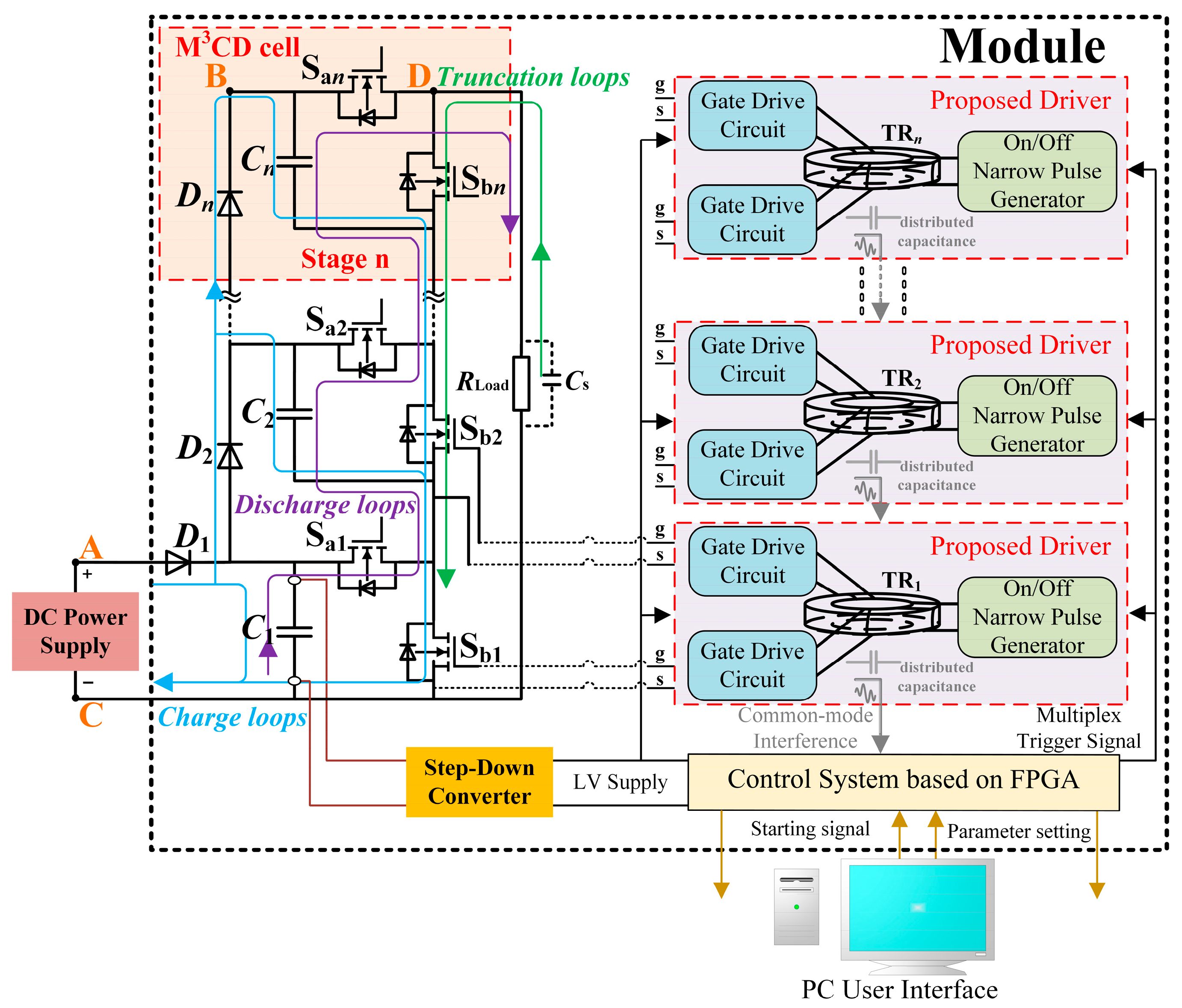
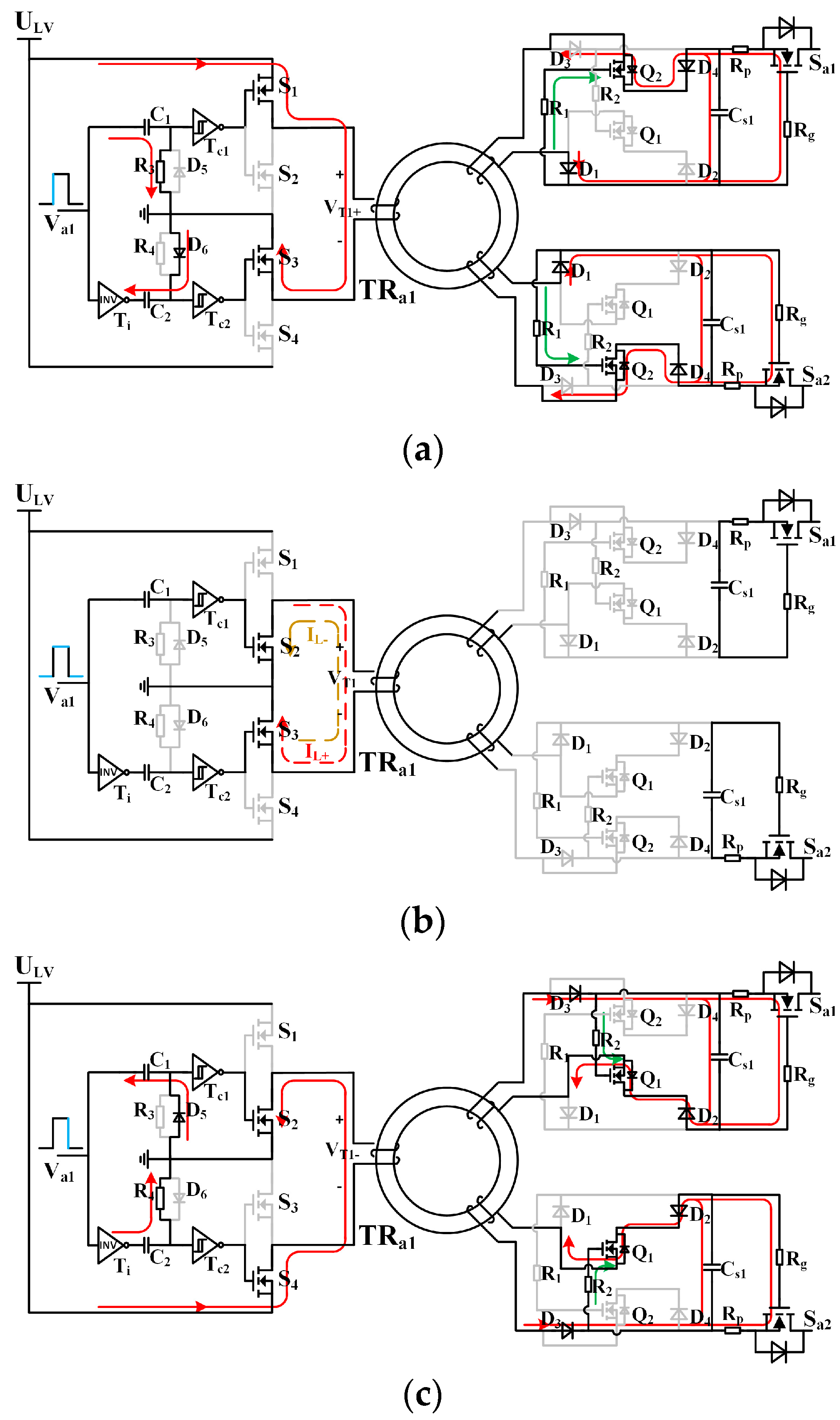
2. The Structure of a Stackable S2M3

Figure 1 shows a flexibly stackable S2M3 structure. An S2M3 comprises a Marx circuit, drivers, a control system, a step-down converter, and an optical fiber communication interface. In the n-stage solid-state Marx circuit topology, high-voltage diodes replace the traditional rechargeable inductors so that the output voltage is not boosted during discharge [32] Each stage of the M3CD cell consists of a high-voltage diode D i , a storage capacitor C i , and a half-bridge structure composed of a charging switch S b i and a discharging switch S a i . When all the charging switches S b i are triggered to switch on, the DC power supply charges all the capacitors in parallel to the specified voltage U C through diode D i , as shown by the blue arrow. However, if a stage S b i is not on, the capacitors C i + 1 after the stage will not be charged. Thus, the voltage U C i on each capacitor can be expressed as follows:
[ U C 1 U C 2 U C 3 U C n 1 U C n ] = [ 1 S b 1 S b 1 S b 2 S b 1 S b 2 S b n 3 S b n 2 S b 1 S b 2 S b n 3 S b n 2 S b n 1 ] [ V dc ]
where S a i or S b i denotes the state of each switch 1 is ON, and 0 is OFF. Simultaneously, the switches S b i provide a low-impedance discharge path for the stray capacitor C s on the load to eliminate the slow tail of the pulse, as indicated by the green arrow.
When the switches S b i are off and the switches S a i are on, all capacitors are connected in series according to the purple arrow to generate a high-voltage pulse on the load. If a stage S a i is not triggered or switched on later than other switches, the current will flow from the body diode of S b i to the load, and the C i fails to enter the discharge loop. The pulse voltage amplitude on load can be expressed as follows:
[ U Load ] = [ S a 1 S a 2 S a 3 S a n 1 S a n ] T [ U C 1 U C 2 U C 3 U C n 1 U C n ]
The circuit has a simple topology, and its modular circuit features enable it to be expanded flexibly [33,34,35,36] to increase output voltage, current, adjustable level number, or generate bipolar positive and negative pulses. In this way, hardware layout and selection are not required, reducing design time and cost. Several expansion modes of power circuits are shown in Figure 2a–d.
Due to common-mode conduction interference, the output pulse amplitude of the generator based on discrete magnetic coupling drivers cannot be very high; however, the proposed driver can achieve a relatively low output pulse amplitude with a minimized volume, which can make the SSMM a compact structure and is conducive to the stacking study of S2M3 at a small volume and low cost. SSMM typically requires an additional DC power supply for the low-voltage control system, a high-frequency charging power supply or a low-voltage DC power supply to provide isolated power to the driver, and a high-voltage DC power supply for the energy storage capacitor. In contrast, discrete magnetically coupled drivers avoid the power consumed by multiple fiber emitters in the control system while eliminating the need to supply power for driver isolation. Therefore, it is convenient to use a step-down DC-DC converter to convert the first-stage storage capacitor from high voltage to low voltage DC to supply power to the control system and drivers. A transistor-transistor logic (TTL) signal is used to realize the closed-loop control of the converter. The way it works makes the reference ground potential of each module change regardless of the output potential relative to the ground of multiple S2M3s; however, it always matches the potential of the low voltage side of its own first-stage energy storage capacitor, which not only avoids exceeding the maximum electrical insulation level of the driver; however, maintains the intensity of the common mode interference of each module control system, which improves the reliability and stability of S2M3 output. In addition, S2M3s only need one external high-voltage DC power supply; therefore, the system is more integrated.
Figure 3 shows the optical fiber communication between modules. To facilitate communication between modules, each module comprises two sets of optical fiber-optic transceivers for communication and synchronous starting. The PC user interface employs UART communication to configure parameters for each module over communication fibers. The starting signal of the module will be calibrated by the main control chip for synchronous starting. Multiple S2M3s transmit starting signals and control signals through optical fiber interconnection to achieve module control and cooperative operation. As the main control chip, an FPGA with excellent synchronization and EMC capability is used. When the FPGA controller in each module receives the synchronous starting signal, it sends trigger signals that determine the S a i and S b i on/off states. By modifying the trigger signal timing sequence, a S2M3 can independently output nanosecond pulse parameters of adjustable rising/falling time, amplitude, pulse width, and frequency, or modules can collaborate to expand the electrical parameter capability.

3. Operation Principle of Proposed S2M3

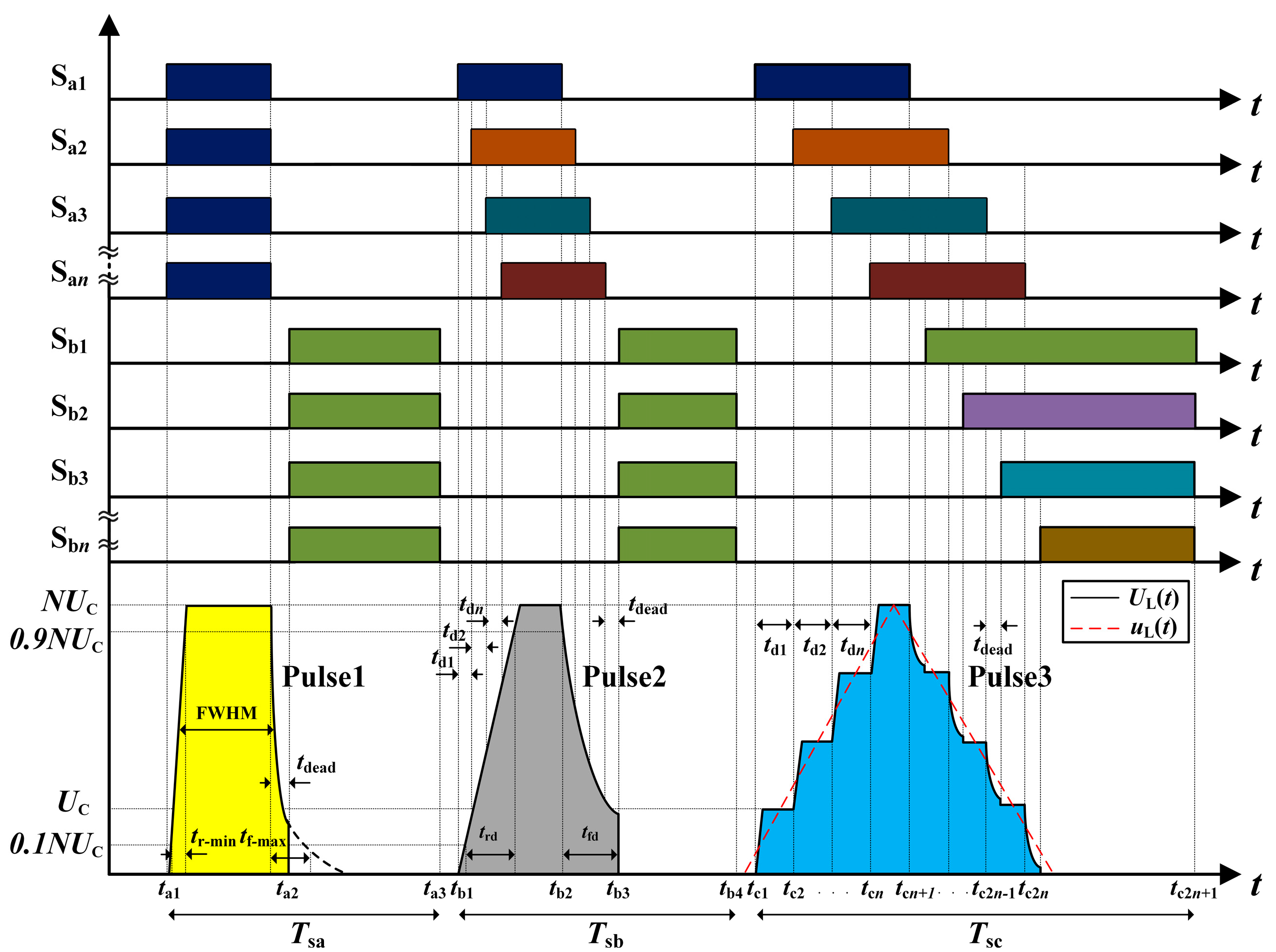
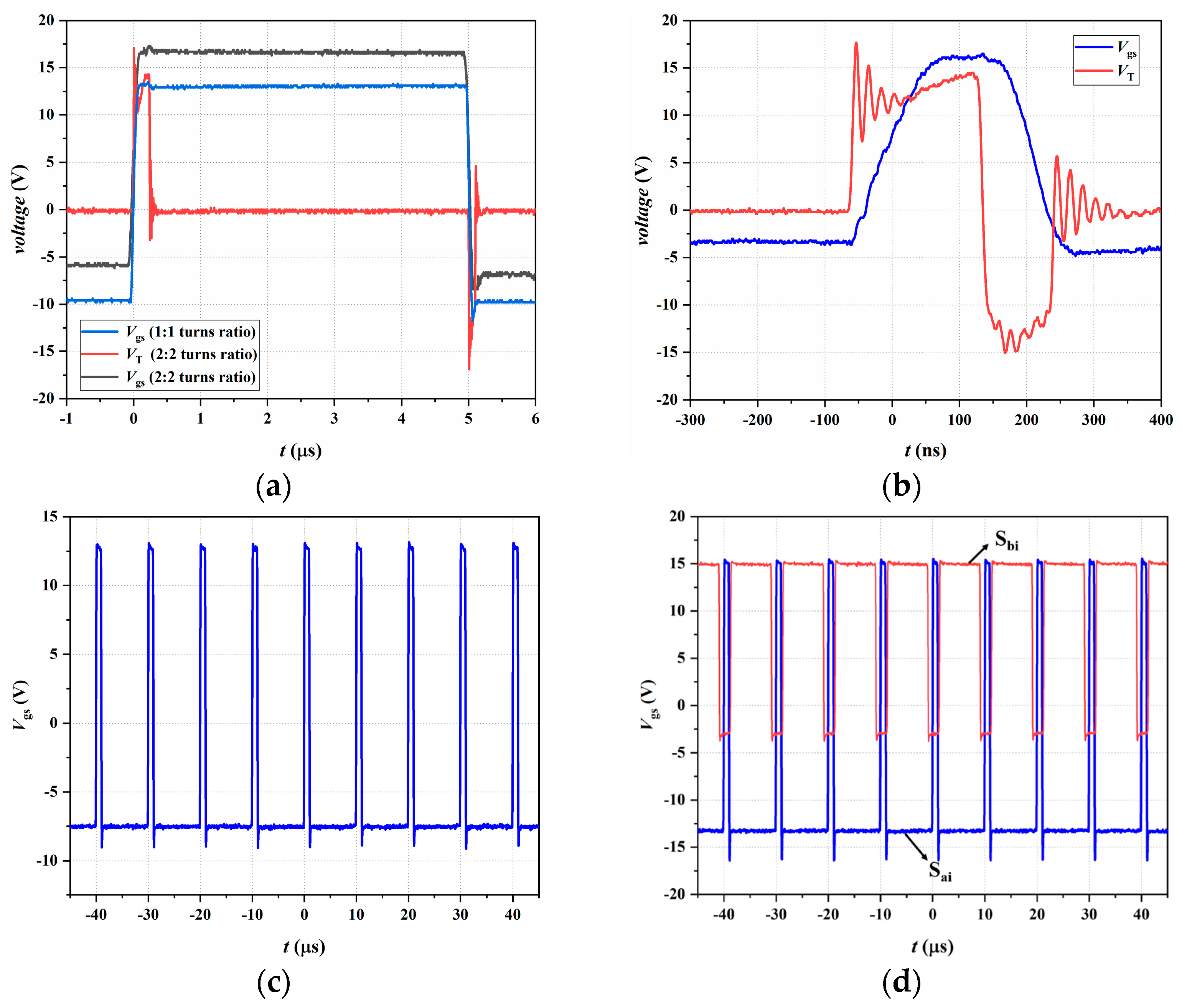
3.1. Switching Timing Sequence under Pulse Modulation

Additional resistors or inductors are inserted into the charging loop to diminish the surge current [15,37]. The values of resistance and inductance are determined by the capacity of the storage capacitor, the charging time, and the number of M3CD cells, which will influence the charging speed and constrain the enhancement of the pulse repetition frequency. Under the magnetic coupling driving condition, there is no need for an additional power system to isolate the power supply, and the benefit of a convenient and controllable driving voltage under the system can be exploited. The driving voltage of the charging switch can be controlled when the initial voltage of the storage capacitor is lower for soft start, so that the S b i can operate in the constant current area to limit surge charging current. In the process of repetition frequency discharge, the S b i can be fully turned on by increasing the driving voltage, which will not affect the charging speed and prevent the cumulative effect of voltage top-up caused by insufficient charging at high repetition frequency. Voltage sensors and other control signals are not required for lower cost and complexity than charging from a current-controlled input source [35] or current source [22].
Since S a i and S b i can be on or off at distinct times, for each M3CD cell, the output pulse waveform is modified by rationally controlling the time when the storage capacitor is inserted or bypassed in the discharge loop, so as to satisfy the demands of different loads. Figure 4 illustrates the time sequence of trigger signals corresponding to three different classical pulse waveforms. It is assumed that the energy-storage capacitor voltage in the three stages is charged to U C before discharge. The specific control timing of key parameters can be explained as follows.
(1) Pulse 1 ( t a 1 t t a 3 ): At time t a 1 switches S a i are turned on simultaneously; when switches S b i are in the off state, the fastest rising edge is obtained on the load, and the rising time is denoted as t r , which is not only proportional to the turn-on time of the MOSFETs but also to the ratio of the stray inductance L s d of the discharge loop and the load resistance R L o a d (see the following formula):
t r L sd / R Load
According to the set duty ratio and pulse repetition frequency, the duration of the trigger signal is regulated and the magnitude of the FWHM is adjusted. t d e a d indicates the dead time between switches S a i and S b i trigger signals to prevent short circuit of the bridge arm in M3CD cells. At time t a 2 , switches S b i turn on while switches S a i are completely off. While the storage capacitors are charging, C s will discharge through S b i to obtain a fast falling edge. Because the t d e a d is so brief, U L ( t ) is approximately a rectangular pulse. Conversely, if switches S b i are not on, the falling time is t f m a x , the voltage of the load can be computed in the following equations:
U L ( t ) = N U C e t R Load C s
t f max = 2.2 R Load C s
(2) Pulse 2 ( t b 1 t t b 4 ): Clearly, if trigger signals fail to have good synchronization, it will affect the rise/fall times of the output pulse [18]. At time t b 1 , S a 1 is switched on, and U C 1 first discharges from the S b 2 body diode to the load. t d i is the relative delay time of each stage of storage capacitor in series or by pass in the discharge loop. Due to the stray inductance and capacitance of the discharge loop, when t d i < t r m i n , the pulse rising time can be adjusted smoothly. For a discharge loop containing an n-stage M3CD cell, t r can be estimated according to the following equation:
t r t r min + i = 1 n 1 t di ( 0 t di t r min )
Similarly, at time t b 2 , S a i delay off, if t d i < t f m a x , the falling time t f can be estimated according to the following equation:
t f t f max + i = 1 n 1 t di ( 0 t di t f max )
After a brief t d e a d , at time t b 3 , the switches S b i are on. Compared with [19] there will be no significant step phenomenon in the control sequence under low resistance loads. When fewer M3CD cells participate in the discharge, t d i should be set shorter to reduce pulse rising/falling edge oscillation [17]. Unlike traditional rectangular pulses, the high-voltage triangular waveform pulse U L ( t ) has a slower, smoother rising and falling edge, reducing EMI in the system. Multiple delay trigger signals instead of prolonged Miller platform duration [38] lower switching losses.
(3) Pulse 3 ( t c 1 t t c 2 n + 1 ): When t d i > t r m i n or t d i > t f m a x , a relatively obvious step wave will appear at the rising/falling edge of the pulse. FIFO control is usually used to achieve capacitor voltage balance. According to the idea of nearest-level modulation, the timing sequence has the ability to mimic u L ( t ) [39]. Different parts of u L ( t ) is approximated by the superposition of equal voltage steps U C produced by each M3CD cell, regardless of what the exact waveform is like in each part. Thus, the insertion of a specific number of capacitors at a certain time interval [ t c i , t c i + 1 ] and [ t c j , t c j + 1 ] can generate an approximate waveform of u L ( t ) . When capacitors are not inserted, u L ( t ) is 0. The switching moments t c i and t c j can be computed according to the following equation:
{ u L ( t ci ) = ( i 1 2 ) U C , i = 1 , 2 , , n u L ( t c j ) = ( 2 n j + 1 2 ) U C , j = n + 1 , n + 2 , 2 n
The above three control modes can be combined freely. When the load changes, the switching timing sequence can be adjusted to match the impedance of the S2M3 with the impedance of the load, and different pulse waveforms can be output to meet the requirements of the load. Compared with adding hardware delay to the drive circuit [21], it has higher accuracy and flexibility.

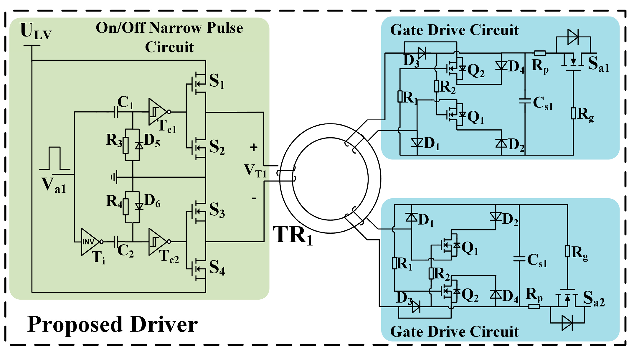
3.2. The Working Process of Proposed Driver

The structure of a discrete magnetic coupling driver is shown in Figure 5. Multiple trigger signals are decomposed by an on/off narrow pulse circuit for a positive turn-on drive signal and a negative turn-off drive signal. The ring transformer will isolate and transmit the drive signal V T to the gate drive circuit for restoration. By adjusting the voltage U L V , the driving voltage amplitude of the switch can be easily changed to realize the switch’s operation in different working areas. The details of the operational principle can be analyzed as shown in Figure 6.
(1) Turn-on Transient State [As Shown in Figure 6a]: Taking the on/off of discharge switches S a 1 and S a 2 as an example. R 3 and C 1 constitute a series RC circuit, as performed C 2 and R 4 . When V a 1 , a trigger signal, reaches a high level, C 1 begins to charge, while C 2 quickly discharges to inverter T i through R 4 paralleling schottky diode D 6 . The speed of discharge is determined by the driving capacity of T i . V T c i H and V T c i L are respectively the high threshold voltage and low threshold voltage of the window comparator T c i . At this point, input voltage V T c 2 i n of V T c 2 is fixed at a negative value equal to forward voltage drop of D 6 , when V T c 2 i n < V T c 2 L , S 3 turns on. The input voltage V T c 1 i n of V T c 1 can be computed according to the following equation:
V Tc 1 _ in = V a 1 e t R 3 C 1
When V T c 1 i n < V T c 1 L , switch S 1 is off, the positive drive signal time t s p can be derived combining Formula (9) as shown in the following equation:
t sp = R 3 C 1 ln V a 1 V Tc 1 - L
On the secondary side of the transformer, the positive drive signal first turns on Q 2 and the current will pass through diodes D 1 and D 4 to the capacitors C s 1 and gate capacitors C g s of switches S a 1 and S a 2 Meanwhile, the gate capacitor of Q 1 is reversely charged, keeping Q 1 at a negative voltage that prevents it from turning on erroneously because the magnetic field energy stored in the magnetic core and the electric field energy stored in the equivalent capacitance will generate a recoil voltage on the secondary side of the transformer after the positive drive signal ends. t s p is limited by the cores, and it needs to meet the following expression [23]:
0 t sp V T d t = 0 B s N β A w d B = N β A w B s
where N is the number of turns on the primary side, β is the packing factor, A w is the cross-sectional area of the magnetic core, and B s is saturation flux.
(2) Turn-on/off Holds State [As Shown in Figure 6b]: Turn-on time T w for switches S a 1 and S a 2 depends on the dead time between the positive and negative drive signals. At the time, Q 1 and Q 2 are off in the dead time, and the electrical power of C s 1 and C g s is unable to be released. If the trigger signal is longer, the V g s holding time is mainly determined by the zero gate voltage drain current I D S S of Q 1 . The maximum conduction time of the switch can be calculated according to the following equations:
T w - max = ( C s 1 + C gs ) ( V T V th ) I DSS
where V t h is the threshold voltage of the switch. C s 1 affects the output pulse width of S2M3 and can reduce bridge arm crosstalk to some extent [40]. Since the primary side inductance of the transformer has a short continuous flow process, an appropriate increase of R 2 in turn-on hold state can further prevent Q 1 from being mistakenly turned on due to the transfer of residual energy in the inductance to the secondary side of the transformer. Moreover, when T w < t s p , the turn-on holds state disappears.
(3) Turn-off Transient State [As Shown in Figure 6c]: When V a 1 is low, the circuit works similarly to the turn-on transient state. S 2 and S 4 are on, and a negative turn-off drive signal appears on the primary side of the transformer. The duration of the negative drive signal t s n can be derived as shown in the following equation:
t sn = R 4 C 2 ln ( V a 1 V Tc 2 _ L )
with Q 1 turns on, the current will charge the V g s to a negative voltage through diodes D 2 and D 3 . The amplitude of the voltage depends on t s n and R 2 . Since there is no discharge circuit on the secondary side of the transformer, V g s stays almost constant. A negative bias voltage makes the switch turn off reliably and reduces the parasitic conduction caused by the MOSFET Miller capacitor to some extent. The anti-EMI capability of the system will be improved.
The proposed driving circuit uses high-speed switching diodes D 1 D 4 to prevent current from flowing through the body diodes of Q 1 and Q 2 . Otherwise, the slow reverse recovery time would cause V g s to drop when positive and negative drive signals reach 0. The short-circuit protection resistor R p limits the short-circuit energy by changing the operating point of the switches S a i in the active region during a fault. The relationship between short circuit current I c and V g s as shown in the following expression:
V gs = V T I c R p
R p is very low and negligible in normal operation. R g reduces the gate voltage oscillation and surge current of the MOSFET in the drive loop.

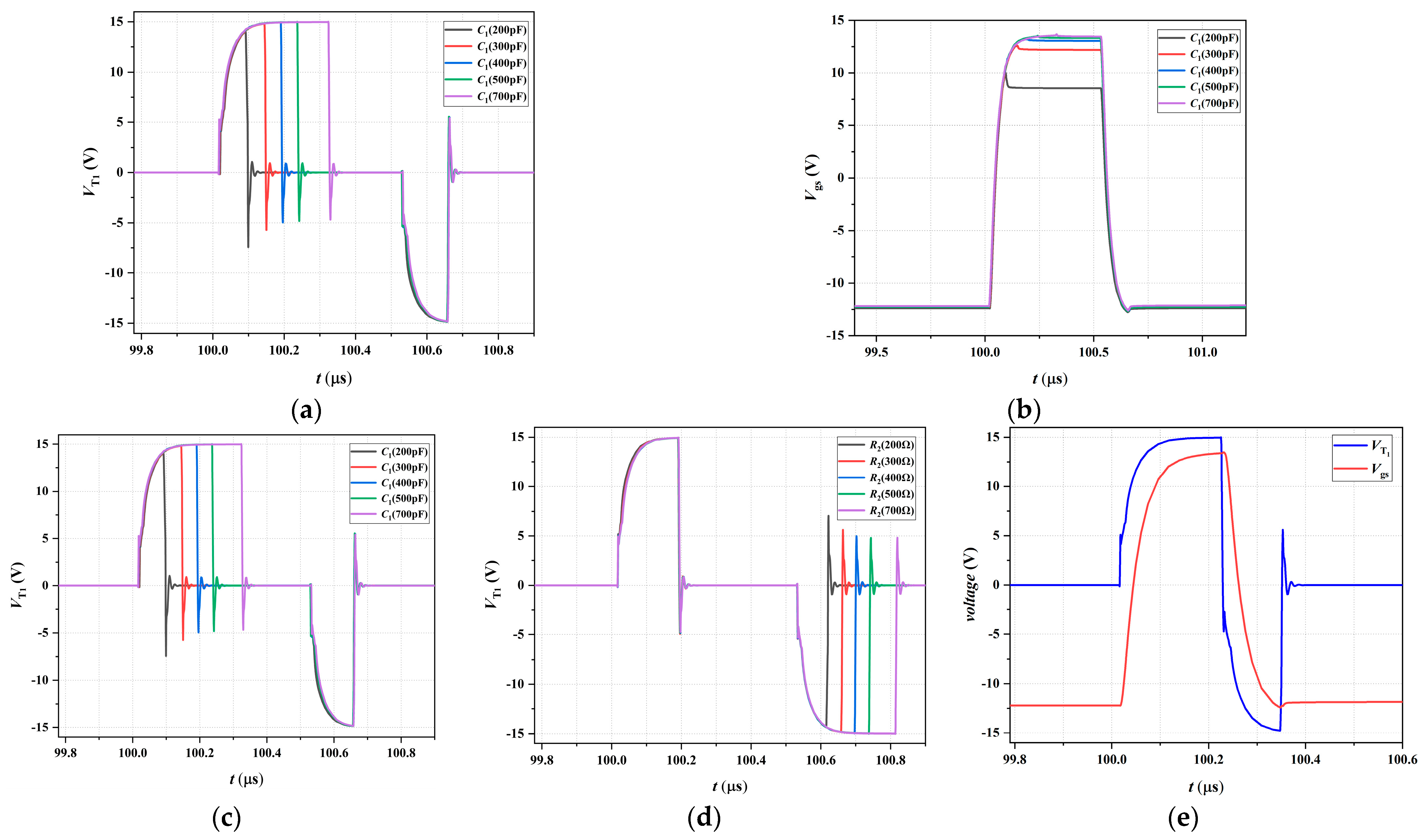
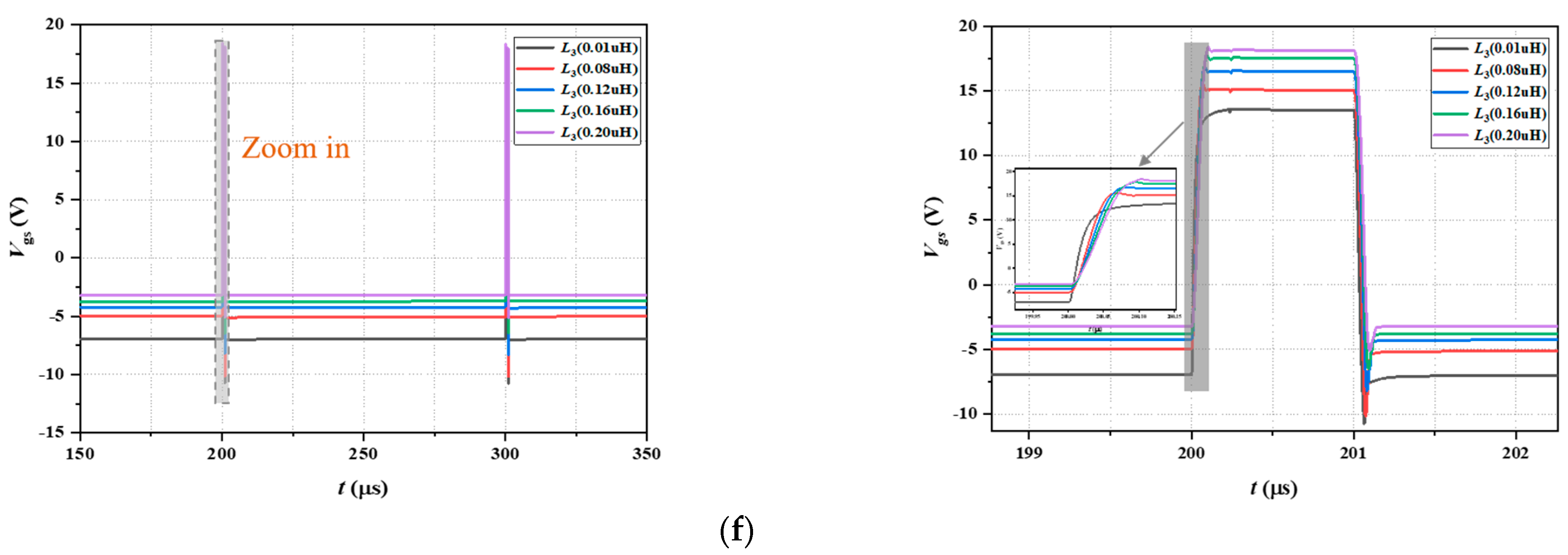
3.3. Simulation of Proposed Driver

A simulation model was established by PSpise 17.4 simulation software, and the influence of changing positive and negative drive signal pulse width and stray inductance on gate voltage was studied by using the global parameter scanning function. Q 1 and Q 2 are PSpice models for the MOSFETs DMG4822SSD provided by the manufacturer. The UCC27517 integrated chip includes a push-pull circuit and Schmidt trigger, with high and low threshold voltages of 2.2 V and 1.2 V, respectively. The specific parameters are shown in Table 2.
When the width of the trigger signal V a 1 is 500 n s . The pulse widths of the different positive drive signals and the corresponding gate voltage are shown in Figure 7a,b. Here, C 1 is 200, 300, 400, 500, 700 p F , respectively. R 1 is 300 Ω . C 2 and R 2 are 300 p F and 300 Ω respectively. The positive drive signal pulse width can be adjusted, and the maximum gate voltage amplitude becomes stable as the drive signal pulse width increases. Figure 7c,d show pulse widths of the different negative drive signals and the corresponding gate voltage. Here, R 2 is 200, 300, 400, 500, 700 Ω , C 1 and R 1 are 300 p F and 400 Ω respectively. Such as the positive drive signals, the reverse voltage is caused by stray inductance L s of the drive loop, and the amplitude of V g s is controllable when the width of the trigger signal V a 1 is 200 n s , and C 1 and R 1 are 400 p F and 900 Ω respectively. Since the pulse width of the trigger signal is smaller than that of the positive drive signal, there is no dead time between the positive and negative drive signals, and the drive signal and the corresponding gate voltages are shown in Figure 7e.
Obviously, the gate voltage will be lower than the drive voltage because of the high-speed switching diodes’ voltage drop and drive resistance in the drive loop on the secondary side of the transformer, which will affect the switching performance of the MOSFETs and the width of the S2M3 maximum output pulse. In the process of setting up the rising edge of the pulse, the stray inductance resonates with the gate capacitance to increase V g s . Figure 7f presents the waveforms of the gate voltage with the different stray inductances, including 0.01, 0.08, 0.12, 0.16, and 0.20 µ H . Here, the pulse width of the trigger signal V a 1 is 1 µ s , C 1 and R 1 are 300 p F and 400 Ω , C 2 and R 2 are 300 p F and 150 Ω .

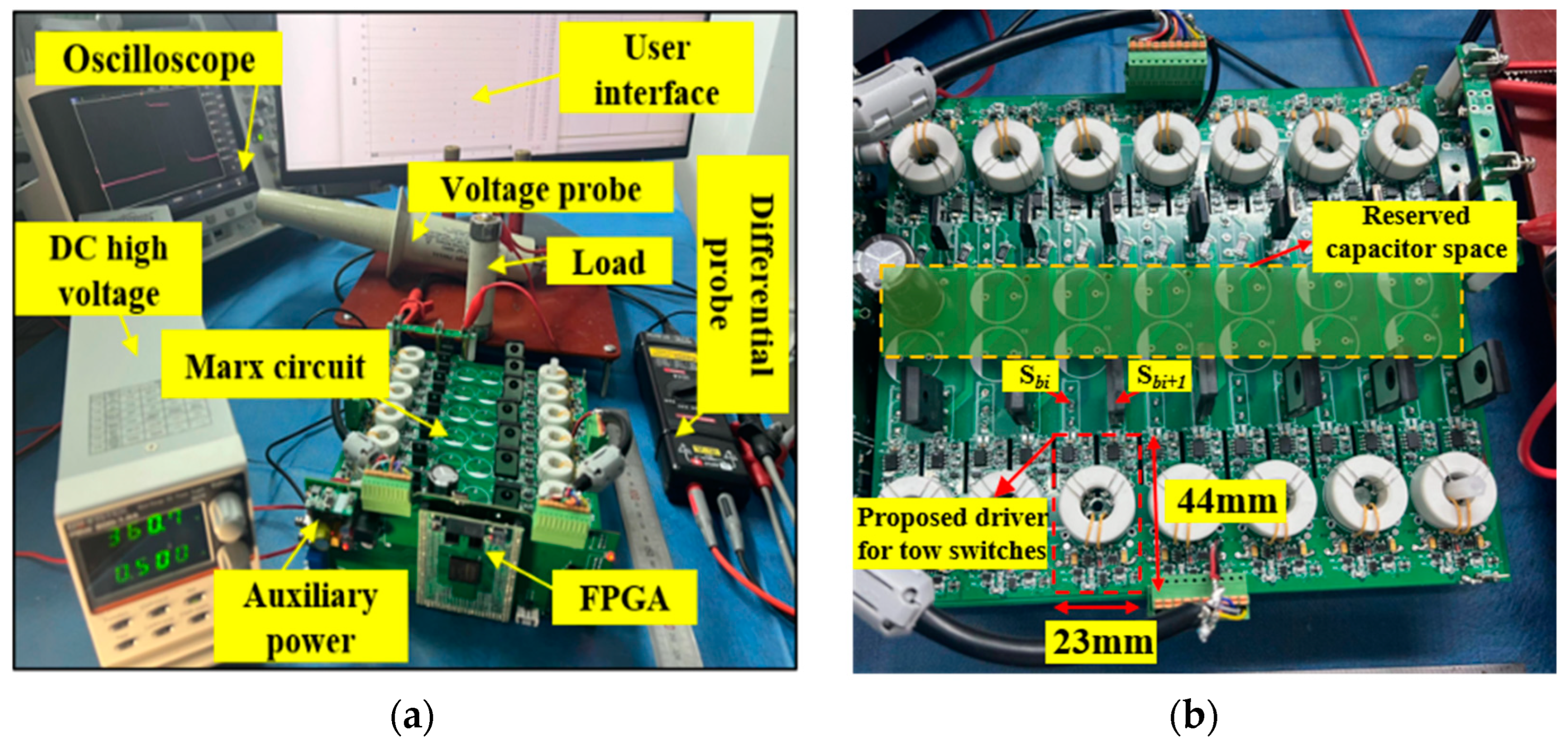
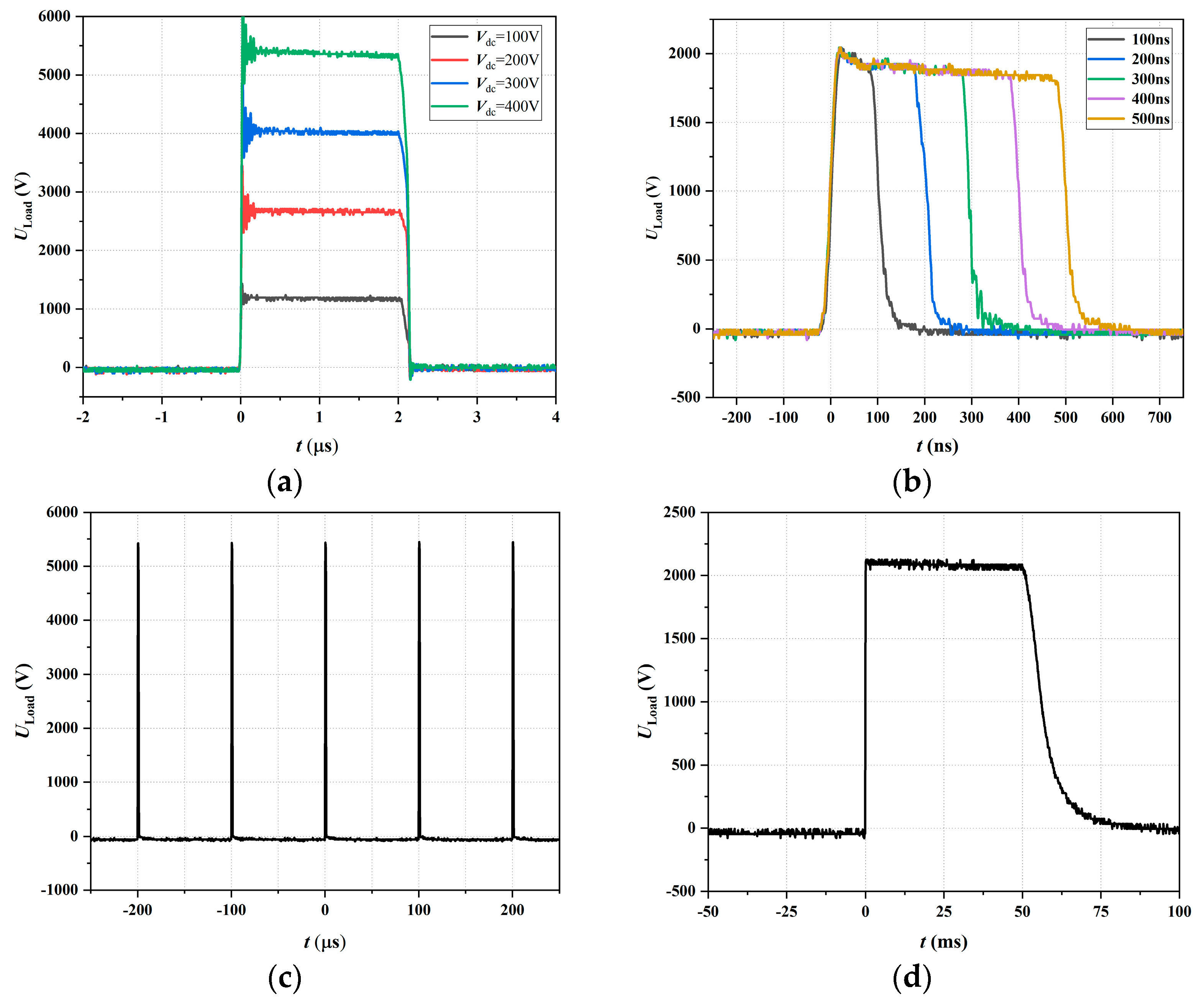
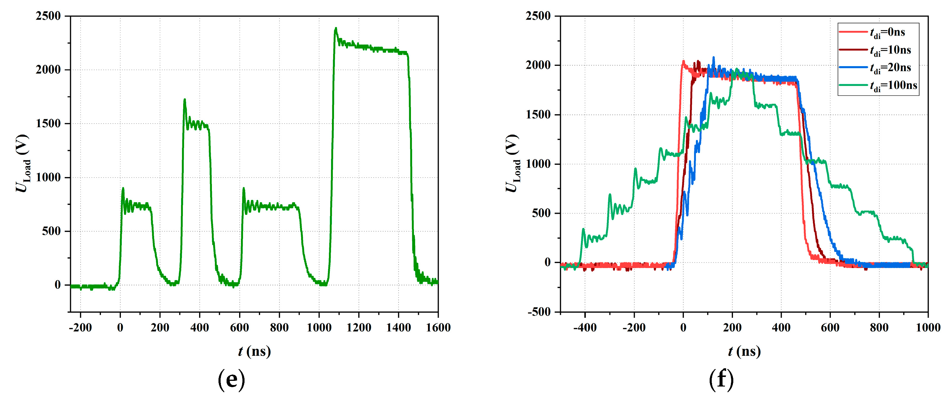
4. Experimental Results

To demonstrate the operation of the proposed S2M3 and validate the simulation structure, a prototype is developed, as shown in Figure 8a. The prototype includes a high-voltage charging power supply, an auxiliary power supply, an FPGA controller, a 14-stage Marx, and a high-voltage output circuit. The auxiliary power supply is a commercial DC-DC converter module that can handle a maximum input DC voltage of 430 V. In Figure 8b, space is reserved in the middle for larger storage capacitors that can remain idle when only a narrow pulse with a fast rising edge is output.
For drivers, the isolation voltage level of each driver depends on the distance between the primary and secondary windings and the insulation strength between the core and the windings. The drivers of each stage operate at a stepped-up ground potential when capacitors discharge in series, and the maximum isolation voltage should be n V d c . The selection of the same size core for each driver guarantees the modularity of the circuit structure. The gate driver and the width and height are implemented within the dimensions of 23 (W) mm × 44 (H) mm, which can be allowed to operate reliably at voltage levels above 10 kV. The driver has stable operation, low circuit loss, and a simple power supply. By sharing a ring core to drive two MOSFETs, it compensates for the lower input voltage of the auxiliary power supply and improves the compactness of the overall volume.
Since the S2M3 outputs a multilevel pulse, the discharge loop passes through the body diode of the charging switches. A long reverse recovery time may exacerbate pulse-rising edge oscillations. Here, the charging switches choose SiC MOSFETs (CMW120R080M1) with a short reverse recovery time. Additionally, since the maximum voltage of switches in actual operation is around V d c , from the perspective of cost, the selection of discharge switches with good on/off characteristics of Si MOSFETs (IPP50R280CE). The amorphous magnetic cores with higher permeability are selected, and the stray inductance of the drive loop is changed by changing the number of turns of the winding.
Differential probe RP1025D (Rigol, Ltd., Soochow, China) was used to test drivers. Here, C 1 and C 2 is 200 p F , R 3 is 960 Ω , R 4 is 360 Ω . As shown in Figure 9a, the primary side waveform of the transformer is a positive and negative narrow pulse. Although the rising/falling edge of gate voltage will slow down when the turns ratio is 2:2, the amplitude of V g s be increased to compensate for driving voltage loss. Figure 9b shows the voltage waveforms of the driver signals and the 200 n s gate voltage at the 2:2 turn ratio. Rapidly increasing and decreasing V g s are crucial for a nanosecond output pulse, where there is no dead time between positive and negative drive signals and slight voltage oscillations are insufficient to affect circuit operation.
Figure 9c visually displays the gate voltage waveform during 100 k H z high repetition operation. The amplitude of gate voltage reduces due to the permeability of the amorphous magnetic core decreasing near 100 k H z . Without replacing the magnetic core material, the magnetic core operating point can be magnetized from the third quadrant of the hysteresis loop by increasing the time of the negative drive signal. As shown in Figure 9d, the blue waveform represents switches’ S a i gate voltage, while the red waveform represents switches’ S b i gate voltage. It can be found that the amplitude of V g s is increased in this way.
The probe was P6015A (Tektronix, Ltd., Beaverton, OR, USA). The oscilloscope used was the DSO-X3024T (bandwidth 200 M H z , Keysight, Ltd., Santa Rosa, CA, USA). Under a 5 k Ω high-voltage noninductive resistor with different V d c , the pulse width is 2 µ s and the frequency is 10 k H z . The load voltage waveform is shown in Figure 10a. When V d c is regulated between 100 V and 400 V , load voltage varies between 1.2 k V and 5.45 k V . With a charging voltage of 400 V , the output voltage efficiency of the generator is 97.3%. The top overshoot of the output pulse is mainly due to underdamped oscillation caused by discharge loop equivalent series inductance and MOSFETs fast switching speeds. Additionally, after the pulse ends, the active pull-down circuit starts working to obtain a rapid falling edge. Figure 10b illustrates the waveforms with widths ranging from 100 to 500 n s . At this time, the charging voltage is set to 150 V , the frequency is 10 k H z , and the load is a 200 Ω high-voltage noninductive resistor. The output pulse’s rising and falling edges with different pulse widths are almost the same. The above can fully verify the pulse amplitude and pulse width, which can be flexibly adjusted.
In order to test the output performance of the generator at high frequency and the ability to output with a long pulse width. In the V d c is 400 V and the load is 5 k Ω , 100 k H z continuous high repetition frequency pulse test result is shown in Figure 10c. It can be proven that stable gate driving is possible. Figure 10d shows a pulse waveform with a pulse width of 50 m s under a no-load condition where the active pull-down circuit is not set to work. The pulse falling edge is about 18 m s which can significantly limit the performance of the S2M3 at high repetition frequencies.
The switching timing sequence of multiplex delay is tested with a 200 Ω load in Figure 10e. Figure 10a shows a pulse train with different voltage amplitudes and pulse widths that can output 2.8 M H z for the burst operation within the safety switching margin by inserting or bypassing varying numbers of capacitors at different times. Figure 10f shows the experimental results of smooth adjustment of the rising and falling edges. There are six turn-on delays. If all turn-on delays t d i are 0 ns, the minimum rising time t r is about 18 n s . When t d i = 10 n s , there is no obvious step phenomenon at the rising edge, and t r is about 68 n s , which is similar to the calculation of Formula (6). When t d i = 20 ns, it is remarkable that there is an obvious step trend in the process of rising edge; however, the trend decreases with increasing numbers of inserted capacitors due to discharge loop stray inductance changes. The step pulse can be generated when t d i = 100 n s . The dynamic adjustment range of t r and t f mainly depends on switching speed and different load parameters. This verifies that the proposed S2M3 can flexibly adjust pulse shapes under the different switch timing sequences as previously described.

5. Conclusions

In this article, a multilevel nanosecond S2M3 based on discrete magnetic coupling drivers is developed, and the following conclusions are drawn.
(1)
The proposed driver uses a magnetic coupling method instead of an optical signal for pulse control there is no need for a separate power source for isolating. As a consequence, the volume and cost of the modulator can be reduced.
(2)
Discrete magnetic coupling drivers have the ability to output long pulse widths and synchronous or delayed driving of all solid-state switches, enabling the pulse generator to change the pulse shape.
(3)
The negative gate voltage amplitude can be adjusted to prevent MOSFET parasitic conduction and ensure its reliable turn-off, and the positive gate voltage amplitude of charging switches can be controlled for soft start.
(4)
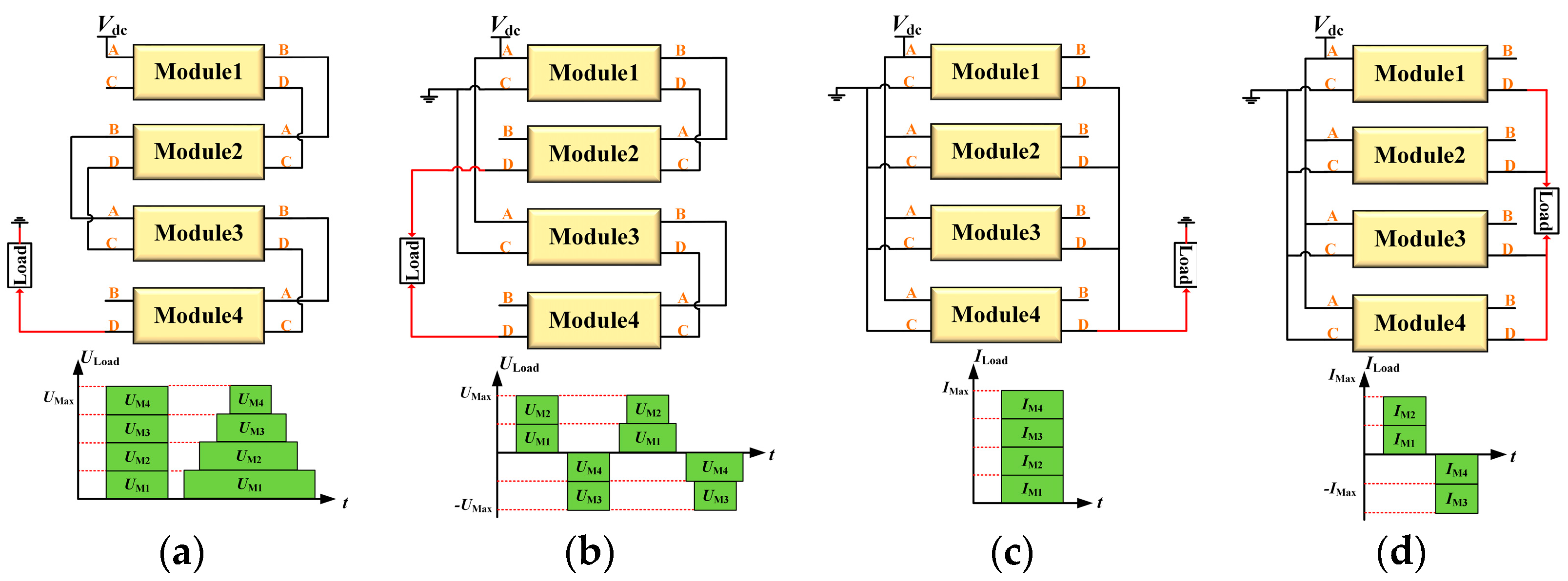
S2M3 has a compact structure and simple communication between modules; the maximum voltage endured by each driver in each S2M3 and its interference intensity to the controller remain constant when modules are serially stacked to generate higher voltage, which facilitates cascading and expansion of voltage and current parameters in the future.
(5)
At present, the output parameters obtained are as follows. The prototype has a voltage amplitude up to 5.45 k V with 100 k H z within the continuation and 2.8 M H z within the burst. The pulse shapes can be altered, and the pulse width is continuously adjustable within 100 n s to 50 m s .
On the other hand, the proposed gate driver is compatible with other solid-state switches. A push-pull circuit with a larger current flow capacity can increase and decrease gate voltage more rapidly, reducing switch synchronization errors and drive pulse width. Furthermore, using ferrite cores with superior high-frequency characteristics can improve pulse repetition frequency.

Author Contributions

Conceptualization, L.C., J.Q. and K.L.; methodology, L.C. and J.Q.; software, L.C.; validation, L.C.; formal analysis, L.C. and H.Z.; investigation, L.C. and J.Z.; writing—original draft preparation, L.C.; writing—review and editing, J.Q., H.Z., K.L. and C.Z.; supervision, J.Q. and H.Z.; project administration, J.Q. All authors have read and agreed to the published version of the manuscript.

Funding

This research was funded in part by the National Natural Science Foundation of China (under Grant No. 51877406).

Data Availability Statement

All the data that supports the findings of this study are included within the article.

Conflicts of Interest

The authors declare no potential conflicts of interests.

References

  1. Rao, X.; Chen, X.; Zhou, J.; Zhang, B.; Alfadhl, Y. Design of a high voltage pulse generator with large width adjusting range for tumor treatment. Electronics 2020, 9, 1053. [Google Scholar] [CrossRef]
  2. Rezanejad, M.; Sheikholeslami, A.; Adabi, J. Modular switched capacitor voltage multiplier topology for pulsed power supply. IEEE Trans. Dielectr. Electr. Insul. 2014, 21, 635–643. [Google Scholar] [CrossRef]
  3. Redondo, L.M.; Silva, J.F. Flyback versus forward switching power supply topologies for unipolar pulsed-power Applications. IEEE Trans. Plasma Sci. 2009, 37, 171–178. [Google Scholar] [CrossRef]
  4. Mei, T.T.; Gao, M.; Wang, Y.; Huang, Y.F.; Chu, P.K. Effects of acid treatment and plasma micromachining on the surface properties of carbon fibers. Appl. Surf. Sci. 2022, 592, 153261. [Google Scholar] [CrossRef]
  5. Yan, Z.; Yin, L.; Hao, C.; Liu, K.; Qiu, J. Synergistic effect of pulsed electric fields and temperature on the inactivation of microorganisms. AMB Express 2021, 11, 47–62. [Google Scholar] [CrossRef] [PubMed]
  6. Pirc, E.; Miklavčič, D.; Uršič, K.; Serša, G.; Reberšek, M. High-frequency and high-voltage asymmetric bipolar pulse generator for electroporation based technologies and therapies. Electronics 2021, 10, 1203. [Google Scholar] [CrossRef]
  7. Florkowski, M.; Blaszczyk, P.; Klimczak, P. Partial discharges in twisted-pair magnet wires subject to multilevel PWM pulses. IEEE Trans. Dielectr. Electr. Insul. 2017, 24, 2203–2210. [Google Scholar] [CrossRef]
  8. Yang, J.; Zhuang, L.; Feng, Y.; Sugai, T.; Jiang, W. Feedback control of pulsed-power generator based on solid-state linear transformer driver. Rev. Sci. Instrum. 2021, 928, 084704–084711. [Google Scholar] [CrossRef]
  9. Jiang, S.; Shi, H.; Wang, Z.; Wang, Y.; Wu, Z.; Li, Z.; Rao, J. A bipolar modular multilevel generator based on half-bridge and special full-bridge for electroporation applications. IEEE Trans. Plasma Sci. 2021, 49, 1920–1927. [Google Scholar] [CrossRef]
  10. Elgenedy, M.A.; Darwish, A.; Ahmed, S.; Williams, B.W. A transition arm modular multilevel universal pulse-waveform generator for electroporation applications. IEEE Trans. Power Electron. 2017, 32, 8979–8991. [Google Scholar] [CrossRef]
  11. Zhong, Z.Y.; Rao, J.F.; Liu, H.T.; Redondo, L.M. Review on solid-state-based Marx generators. IEEE Trans. Plasma Sci. 2021, 49, 3625–3643. [Google Scholar] [CrossRef]
  12. Rocha, L.L.; Silva, J.F.; Redondo, L.M. Marx multilevel bipolar modulator dynamic models for load transient analysis. IEEE Trans. Plasma Sci. 2017, 45, 2611–2617. [Google Scholar] [CrossRef]
  13. Rocha, L.L.; Silva, J.F.; Redondo, L.M. Seven-level unipolar/bipolar pulsed power generator. IEEE Trans. Plasma Sci. 2016, 44, 2060–2064. [Google Scholar] [CrossRef]
  14. Rocha, L.L.; Silva, J.F.; Redondo, L.M. Multilevel high-voltage pulse generation based on a new modular solid-state switch. IEEE Trans. Plasma Sci. 2014, 42, 2956–2961. [Google Scholar] [CrossRef]
  15. Yao, C.; Zhang, X.; Guo, F.; Dong, S.; Mi, Y.; Sun, C. FPGA-controlled all-solid-state nanosecond pulse generator for biological applications. IEEE Trans. Plasma Sci. 2012, 40, 2366–2372. [Google Scholar] [CrossRef]
  16. Kandratsyeu, A.; Sabaleuski, U.; Redondo, L.; Pakhomov, A.G. Four channel 6.5 kV, 65 A, 100 ns-100 us generator with advanced control of pulse and burst protocols for biomedical and biotechnological applications. Appl. Sci. 2021, 11, 11782. [Google Scholar] [CrossRef]
  17. Mi, Y.; Wan, H.; Bian, C.; Peng, W.; Gui, L. An MMC-based modular unipolar/bipolar high-voltage nanosecond pulse generator with adjustable rise/fall time. IEEE Trans. Dielectr. Electr. Insul. 2019, 26, 515–522. [Google Scholar] [CrossRef]
  18. Liu, Y.; Fan, R.; Zhang, X.; Tu, Z.; Zhang, J. Bipolar high voltage pulse generator without H-bridge based on cascade of positive and negative Marx generators. IEEE Trans. Dielectr. Electr. Insul. 2019, 26, 476–483. [Google Scholar] [CrossRef]
  19. Fan, R.; Wang, Y.; Zhang, X.; Tu, Z.; Zhang, J. Parameterized nanosecond pulse realization through parametrical modulation of timing sequence of switches in Marx circuit. IEEE Trans. Plasma Sci. 2019, 47, 4096–4104. [Google Scholar] [CrossRef]
  20. Park, S.-M.; Song, S.-H.; Jo, H.-B.; Jeong, W.-C.; Jang, S.-R.; Ryoo, H.-J. Solid-state pulsed power modulator for 9.3 GHz 1.7 MW X-band magnetron. IEEE Trans. Ind. Electron. 2021, 68, 1148–1154. [Google Scholar] [CrossRef]
  21. Li, Z.; Liu, H.T.; Jiang, S.; Rao, J.F. A new driving circuit with delay trigger for the solid-state Marx modulators. IEEE Trans. Plasma Sci. 2021, 49, 1906–1914. [Google Scholar] [CrossRef]
  22. Jo, H.-B.; Song, S.-H.; Lee, S.-H.; Ryoo, H.-J. MOSFET gate driver circuit design for high repetitive (200 kHz) high voltage (10 kV) solid-state pulsed-power modulator. IEEE Trans. Power Electron. 2021, 36, 10461–10469. [Google Scholar] [CrossRef]
  23. Zhou, Z.; Li, Z.; Rao, J.; Jiang, S.; Sakugawa, T. A high-performance drive circuit for all solid-state Marx generator. IEEE Trans. Plasma Sci. 2016, 44, 2779–2784. [Google Scholar] [CrossRef]
  24. Gao, L.; Wang, D.; Qiu, J.; Liu, K. All-solid-state pulse adder with bipolar high voltage fast narrow pulses output. IEEE Trans. Dielectr. Electr. Insul. 2011, 18, 775–782. [Google Scholar] [CrossRef]
  25. Zeng, W.; Yao, C.; Dong, S.; Wang, Y.; Ma, J.; He, Y.; Yu, L. Self-triggering high-frequency nanosecond pulse generator. IEEE Trans. Power Electron. 2020, 35, 8002–8012. [Google Scholar] [CrossRef]
  26. Yan, J.; Shen, S.; Ding, W. High-power nanosecond pulse generators with improved reliability by adopting auxiliary triggering topology. IEEE Trans. Power Electron. 2020, 35, 1353–1364. [Google Scholar] [CrossRef]
  27. Rao, J.; Song, Z.; Wang, Y.; Song, J.; Li, Z. Sub-microsecond high voltage pulse power supply based on magnetic isolated driving. High Power Laser Part. Beams 2021, 33, 171–177. [Google Scholar]
  28. Canacsinh, H.; Redondo, L.M.; Silva, J.F. New solid-state Marx topology for bipolar repetitive high-voltage pulses. In Proceedings of the 2008 IEEE Power Electronics Specialists Conference, Rhodes, Greece, 15–19 June 2008; pp. 791–795. [Google Scholar]
  29. Wu, F.; Zhao, L.; Dong, S.; Zhou, X.; Zeng, W.; Yao, C.; Yu, L. Magnetic coupling resonant-based air-Isolated module for high voltage pulse generators. IEEE Trans. Ind. Electron. 2023, 70, 2431–2439. [Google Scholar] [CrossRef]
  30. Abadi, M.R.Q.R.; Marzebali, M.H.; Abolghasemi, V.; Anisi, M.H. High-voltage pulse generators for electroporation applications: A systematic review. IEEE Access 2022, 10, 64933–64951. [Google Scholar] [CrossRef]
  31. Xie, L.; Ruan, X.; Ye, Z. Equivalent Noise Source: An Effective Method for Analyzing Common-Mode Noise in Isolated Power Converters. IEEE Trans. Ind. Electron. 2016, 63, 2913–2924. [Google Scholar] [CrossRef]
  32. Zeng, W.; Yu, L.; Dong, S.; Ma, J.; Wang, Y.; He, Y.; Wang, X.; Yao, C. A novel high-frequency bipolar pulsed power generator for biological applications. IEEE Trans. Power Electron. 2020, 35, 12861–12870. [Google Scholar] [CrossRef]
  33. Li, Z.; Liu, H.; Jiang, S.; Guo, L.; Rao, J. A high-current all-solid-state pulse generator based on Marx structure. IEEE Trans. Plasma Sci. 2020, 48, 3629–3636. [Google Scholar] [CrossRef]
  34. Redondo, L.M.; Zahyka, M.; Kandratsyeu, A. Solid-state generation of high-frequency burst of bipolar pulses for medical applications. IEEE Trans. Plasma Sci. 2019, 47, 4091–4095. [Google Scholar] [CrossRef]
  35. Elgenedy, M.A.; Massoud, A.M.; Ahmed, S.; Williams, B.W.; McDonald, J.R. A modular multilevel voltage-boosting marx pulse-waveform generator for electroporation applications. IEEE Trans. Power Electron. 2019, 34, 10575–10589. [Google Scholar] [CrossRef]
  36. Shi, H.Z.; Lu, Y.D.; Gu, T.Y.; Qiu, J.; Liu, K.F. High-voltage pulse waveform modulator based on solid-state Marx Generator. IEEE Trans. Dielectr. Electr. Insul. 2015, 22, 1983–1990. [Google Scholar] [CrossRef]
  37. Veilleux, E.; Ooi, B.T.; Lehn, P.W. Marx dc–dc converter for high-power application. IET Power Electron. 2013, 6, 1733–1741. [Google Scholar] [CrossRef]
  38. Rao, J.; Zhang, R.; Shi, F.; Zhuang, L.; Ji, Z.; Zhuang, J. A high-voltage solid-state Marx generator with adjustable pulse edges. High Volt. 2023, 1–11. [Google Scholar] [CrossRef]
  39. Lin, L.; Lin, Y.; He, Z.; Chen, Y.; Hu, J.; Li, W. Improved nearest-level modulation for a modular multilevel converter with a lower submodule number. IEEE Trans. Power Electron. 2016, 31, 5369–5377. [Google Scholar] [CrossRef]
  40. Laird, I.; Yuan, X. Analysing the crosstalk effect of SiC MOSFETs in half-bridge arrangements. In Proceedings of the 2019 IEEE Energy Conversion Congress and Exposition (ECCE), Baltimore, MD, USA, 28 November 2019; pp. 367–374. [Google Scholar]
Figure 1. A flexibly stackable S2M3 structure.
Electronics 12 03831 g001
Figure 2. Expansion modes of the power circuit. (a) Output voltage boosting topology. (b) Output current increased structure. (c) Bipolar pulse topology with output current increased. (d) Bipolar pulse topology with output voltage increased.
Electronics 12 03831 g002
Figure 3. The optical fiber communication and synchronous starting between S2M3s.
Electronics 12 03831 g003
Figure 4. The switching timing sequence of trigger signals corresponds to three different classical pulse waveforms.
Electronics 12 03831 g004
Figure 5. Structure of a discrete magnetic coupling driver.
Electronics 12 03831 g005
Figure 6. Three different working conditions. (a) Turn-on transient state. (b) The turn-on/off state holds. (c) Turn off the transient state.
Electronics 12 03831 g006
Figure 7. (a) The different positive drive signals. (b) V g s correspond to different positive drive signals. (c) The different negative drive signals. (d) V g s correspond to different negative drive signals. (e) Drive signal without dead time and the corresponding V g s . (f) Gate voltage waveform with the different stray inductances.
Electronics 12 03831 g007aElectronics 12 03831 g007b
Figure 8. (a) Experimental prototype. (b) The layout and size of the proposed driver.
Electronics 12 03831 g008
Figure 9. (a) Voltage waveforms of the drive signal and 5 µs width of S a i gate voltage with the different turns ratio. (b) Voltage waveforms of the drive signal and 200 ns width of S a i gate voltage. (c) S a i gate voltage waveform during operation as 100 kHz high repetitive. (d) Improved gate voltage waveforms for S a i and S b i .
Electronics 12 03831 g009
Figure 10. (a) The waveforms of output voltage adjustment. (b) The waveforms of pulse width adjustment. (c) Pulse voltage train with 100 kHz and 1 µs width. (d) Output waveform with a 50 ms width when the active pull-down circuit is idle. (e) A voltage waveform with various pulse widths and amplitudes in one burst. (f) Voltage waveforms with different rise/fall times.
Electronics 12 03831 g010aElectronics 12 03831 g010b
Table 1. Comparison of drivers for solid-state pulse generators.
Type of DriversNon-Isolated Power SupplyIndependent Control of All SwitchesInsulation ReliabilityLow CostLow VolumeRef
Optocoupler driver×+++++[16]
Optical fibers driver×+++++[9,15,17,18,19]
Series-core magnetic coupling driver×+++++++++[20,21,22,23,24]
Self-triggered driver×+++++++++[25,26]
Opto-magnetic driver++++[27]
Proposed driver++++++++
Note: the number of “+” represents the evaluation level.
Table 2. Main simulation parameters of the driver.
ParameterValue
R 1 , R 2 1 Ω
C s 1 , C g s 3 n F
R g 3 Ω
R p 0.08 Ω
Disclaimer/Publisher’s Note: The statements, opinions and data contained in all publications are solely those of the individual author(s) and contributor(s) and not of MDPI and/or the editor(s). MDPI and/or the editor(s) disclaim responsibility for any injury to people or property resulting from any ideas, methods, instructions or products referred to in the content.

