Abstract
Space-based communications at the very high frequency (VHF) band for air traffic management is a new technology application under development that requires energy-efficient architectures to mitigate the power limitations of satellite platforms. The usage of high-efficiency radiofrequency (RF) transmitters can help reduce the power consumption, but nonlinearities concerning the amplified signal in wide fractional bandwidth systems are a problem to solve. This paper proposes a high-efficiency (RF) power amplifier (PA) for satellite communications at the VHF band that aims to reduce the envelope distortion inherent to wide fractional bandwidth multicarrier polar-mode transmitters. Its design is based on a solution called hybrid-coupled switching voltage PA in combination with gallium nitride (GaN) high electron mobility transistor (HEMT) technology. The developed VHF PA prototype delivers up to 95 W from a 28 V power supply, with a drain efficiency about 80% within the 118 MHz to 138 MHz operating band. To test its linearity performance, operating in a polar-mode configuration, a GaN-based wideband envelope amplifier (EA) has been developed to modulate the RF PA supply port. This EA improves its power efficiency by combining it with a slow envelope power supply (SEPS). Some measurements have been taken for a 100 W peak envelope power (PEP) and 10 MHz (maximum carrier spacing) four-tone digitally-modulated test signal, where any distortion product is attenuated 46 dB below the average power of the amplified signal without applying any digital predistortion (DPD) technique.
1. Introduction
It may come as a surprise that in the era of wideband personal digital communications (Long-Term Evolution, 5G, etc.), commercial aviation is still using analog radio systems, with no change in sight, at least in the next few years. This is due to the enormous inertia imposed by the need for international coordination agreements for the adoption of any kind of change, so that any new aeronautical communications system that succeeds should at least be compatible with the traditional system that has been used for the last decades.
Recently, new projects have been undertaken that seek to achieve the global ranges provided by satellite communication systems, while maintaining compatibility with traditional communication systems at the very high frequency (VHF) band. These services are a new developing technology to improve air traffic management, especially in remote areas and oceanic areas where terrestrial infrastructures cannot provide adequate coverage. Since it is not possible to achieve high directivity gains in VHF antennas of sizes suitable for deployment on a satellite, most of the burden of achieving signal levels suitable for this type of service falls on the satellite transponder power amplifiers (PAs).
These systems, based on the aggregation of several communication channels, result in wide fractional bandwidth (i.e., the signal bandwidth divided by the center operating frequency and expressed as a percentage) multicarrier signals with high peak-to-average power ratios (PAPRs). The required linearity figures for the transmitter cause the radiofrequency (RF) PA to operate in a linear mode away from the saturation region, where higher energy efficiency could be obtained. This results in low-energy-efficiency figures for the transmitter if conventional RF PA architectures are used [1].
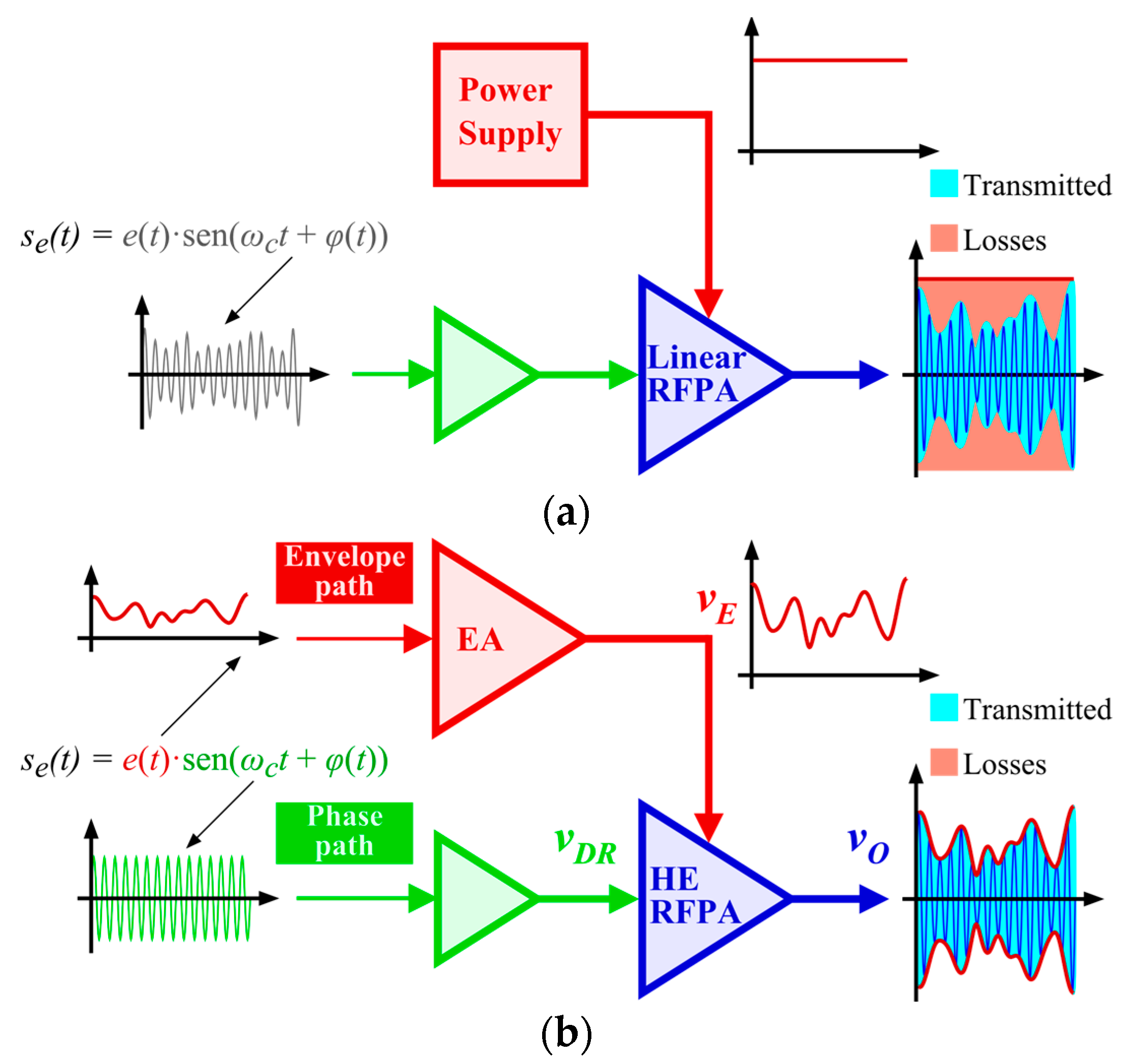
The limited power resources of satellite platforms (due weight and size limitations for economic reasons) require energy-saving transmitters, while the distortion of the amplified signals must be kept to a minimum. There are some linearization techniques that allow the RF PA to operate near or under saturation conditions, while preserving its linearity [2]. As a result, these linearization methods help to increase the power efficiency of RF PAs. One solution that can potentially provide very good power efficiency results at the VHF band is polar-mode PAs [3,4,5,6,7], which have been studied over the course of many years. This technique (that sometimes can also be known as envelope elimination and restoration, or the Kahn technique) basically consists of a combination of a high-efficiency envelope amplifier (EA) that modulates the power supply port of a high-efficiency RF PA, where the amplitude modulation of the RF carrier takes place (high-level modulation principle). Figure 1 graphically compares a conventional transmitter PA (powered by a constant-level voltage supply) and a polar-mode PA architecture. The main advantage of using a polar-mode modulation technique is that, since the RF PA operates in saturation, the level of the amplified signal at the output of the PA (vO) depends on its drain supply voltage (vE) and not on the input signal (vDR), meaning that a high-efficiency switchmode RF PA (class-D, class-E, etc.) can be used.

Figure 1.
Illustrations of power efficiency in RF PA transmitters: (a) power losses in a conventional linear-mode RF PA and (b) power loss representation in a polar-mode RF PA architecture.
When using polar-mode linearization systems at VHF, it must be noted that even moderate bandwidth communications signals exhibit a very wide fractional bandwidth. This poses an additional problem to those associated with EA and RF PAs for polar-mode operation with wideband signals: the RF PA power port must handle wideband envelope signals, while maintaining isolation of the RF output port. This is a major challenge that is still unresolved at these relatively low operating frequencies (VHFs), far removed from the microwave frequency bands, where most research effort and resources are currently focused on envelope tracking (ET) techniques [8,9].
To perform the simulations and tests of this work, a set of modulated signals that model the nature of the multicarrier signals of real systems were used. These signals are composed of several analog or digitally modulated channels within the VHF airband. In the case of analog channels, 10 kHz sine wave amplitude modulated (AM) signals with 80% modulation depth were selected. For the digital channels, a signal emulating the dynamic behavior of VHF data link (VDL) signals such as those used in this type of system was generated. This digital modulation is a differential 8-phase shift keying (D8PSK), at an RS = 10 kBd symbol rate and using a raised cosine shaping filter with an α = 0.6 roll-off factor. In the following sections, these analog and digital modulations for the tests that were performed are referred to as AM-T and VDL-T, respectively. The transmitted signal can be composed of one (1C-CH), two (2C-CH), three (3C-CH), or four (4C-CH) concurrent channels.
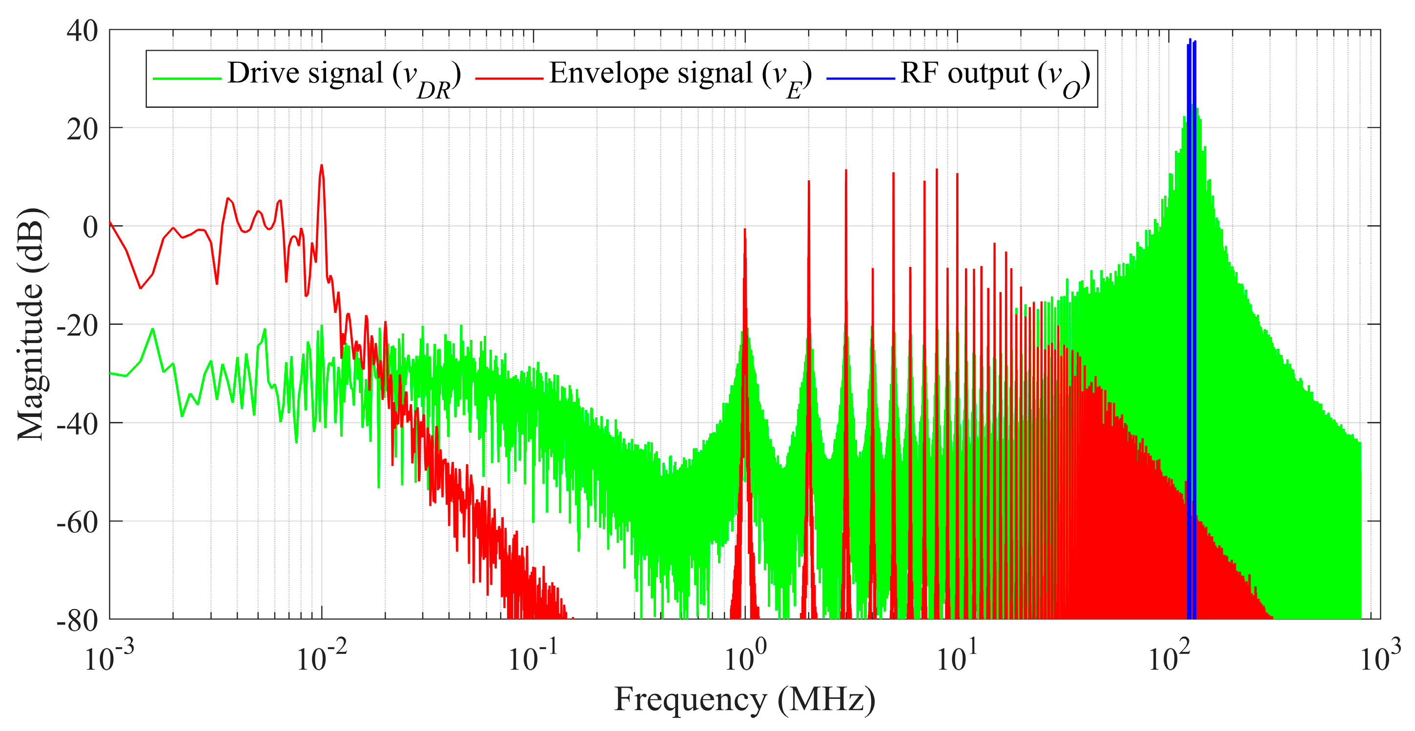
To provide some perspective, in Figure 2 the MATLAB-generated power spectral density (PSD) of the main signals (120 MHz, 123 MHz, 128 MHz, and 130 MHz concurrent VDL-T channels) in a polar-mode transmitter shows the demanding power bandwidth requirements of a multicarrier signal, where the large fractional bandwidth required, together with a power spectral density (PSD) of the signal envelope that exhibits high energy content at high frequencies (which increases the dynamic demands of the envelope path), is a concern that leads to a careful choice of the RF amplifier drain supply (vE) network.

Figure 2.
Power spectral density (PSD) of the 4C-CH VDL-T signal generated by MATLAB. Main signals in a polar-mode transmitter: drive signal (vDR), amplified envelope (vE), and amplified RF signal at the output (vO).
Taking this into consideration, this work shows a way of overcoming the problems associated with wide fractional bandwidth VHF polar-mode PAs that allow for good linearity figures to be achieved for the application described.
This work is mainly divided into three sections. In the first one, a GaN push–pull class-D PA topology is analyzed, proposed, and implemented to mitigate the distortions of the polar systems originating from the RF PA. In the second section, to verify that the implemented RF PA behaves as expected under high-level amplitude modulations (polar-mode architecture), a wideband high-performance GaN-based EA is designed and implemented with a dynamic performance that is sufficient to amplify the signals used for the tests. The third part shows the results obtained from the polar-mode PA, which consists of the integration of the RF PA and the EA implemented in the previous parts.
2. Class-D PA for Polar-Mode Architectures
Since the polar-mode architecture requires the RF PA to be used as a high-level amplitude modulator, it can be considered a three-port device [5,6], as follows:
- The RF drive (vDR) input port, where the carrier (with phase information if required) is injected.
- The envelope (vE) input port is used to modulate the PA with amplitude information.
- The amplified signal (vO) is provided by the RF output port.
The difficulty of achieving good isolation (from unwanted signal components) between ports results in some distortion problems that usually affect the amplified signal (vO) envelope; this is due to the leakage from the input ports (vDR and vE) to the RF output port and the bandwidth limitations of the envelope input port (vE).
2.1. Envelope Nonlinearities in Polar-Mode RF PAs
Regarding the RF input port (vDR), the drive feedthrough effect has been widely covered [10]. However, the literature content is less focused on the distortion affecting the envelope input port because this issue is only present in high-fractional-bandwidth transmitters.
The class-D PA (Figure 3) is a good candidate for this application since it combines high-efficiency and wideband operation with design flexibility, which allows the user to choose the best structure to prevent nonlinearities related to the envelope path. The basic idea of the class-D operation is to use a square signal sC(t), as follows:
to drive a switchmode power stage, its amplified output is applied to a resonator that removes its harmonic components. This resonator may consist of a low-Q LC circuit that acts as a wide bandpass filter to allow for the use of wideband modulations.

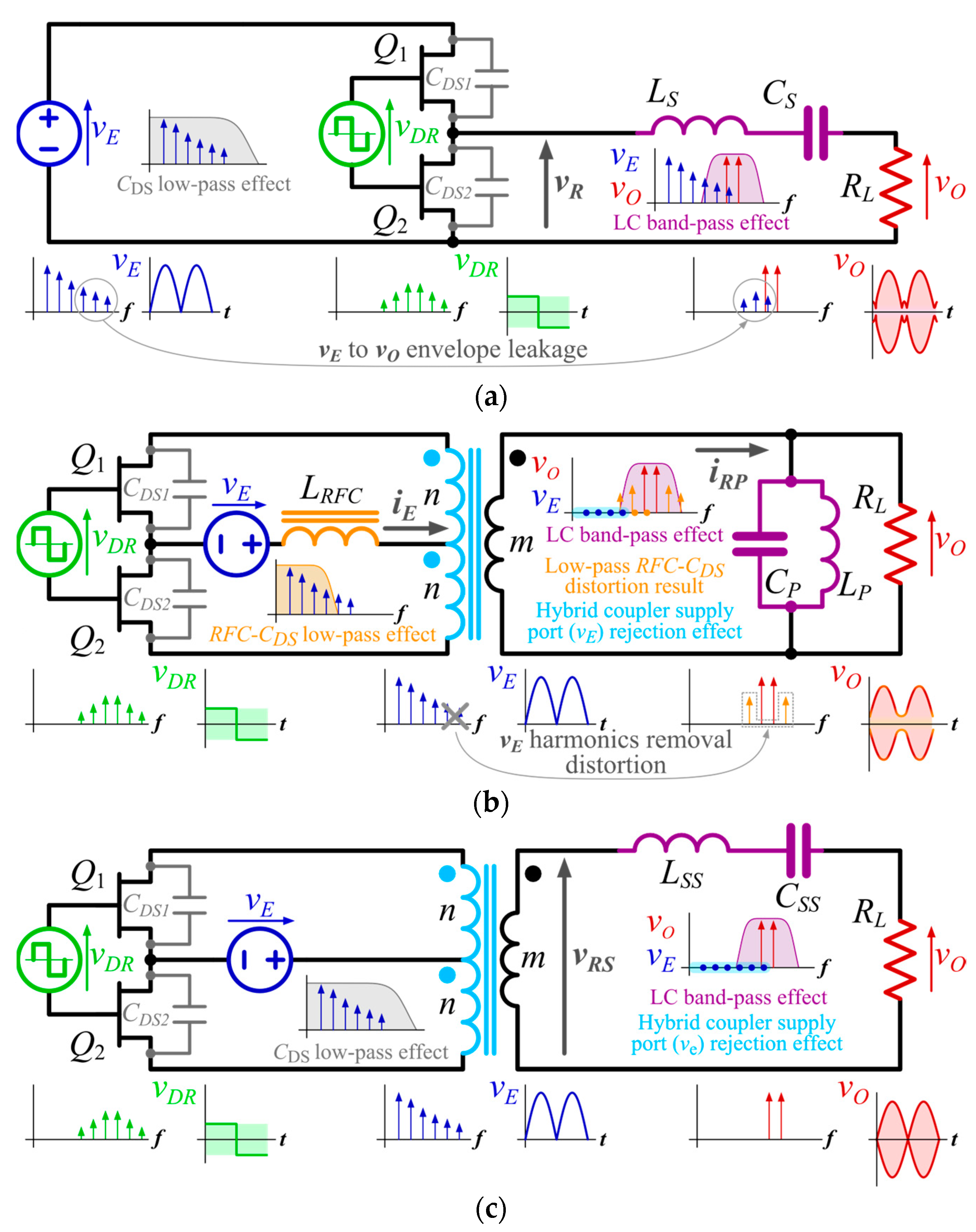
Figure 3.
Linearity behavior of the envelope for different switchmode RF PAs operating in polar mode: (a) Class-D CVS, (b) Class-D TCCS, and (c) Class-D TCVS.
In support of this idea, the following sections analyze, in a simplified and graphical form, the nonlinearities that concern the envelope (vE) path for the three class-D PA topologies described in the literature [11,12,13,14]. Based on [12], Equations (1)–(9) help to describe the behavior of these circuits.
2.1.1. Class-D Complementary Voltage Switching
The complementary voltage switching (CVS) topology [14,15], as shown in Figure 3a, requires a low-Q resonator (LS, CS) at its load network to allow for wideband operation. Consequently, the envelope input (vE) baseband (independent term) component present at the resonator input (vR) is defined as follows:
It cannot be fully suppressed by the low-Q resonator, resulting in some envelope leakage (vE to vO) at the output (vO). This issue is also present in any single-ended PA topology.
2.1.2. Class-D Transformer-Coupled Current Switching
The transformer-coupled current switching (TCCS) topology [16,17], as shown in Figure 3b, is a widely used topology that helps to mitigate the nonlinearities related to the envelope leakage (vE to vO) effect. Its push–pull operation theoretically cancels the envelope current (iE) baseband component before being applied (iRP) to the low-Q resonator (LP and CP), as seen in the following:
where the envelope-independent term (iE) was removed.
However, the current-feeding inductor (LRFC) required to operate from a voltage source (vE) limits its bandwidth in wideband applications, resulting in spectral regrowth of the amplified signal (vO).
2.1.3. Class-D Transformer-Coupled Voltage Switching
In the transformer-coupled voltage switching (TCVS) PA [18,19], which is shown in Figure 3c, the input envelope (vE) is directly applied to the transformer. This fixes the limited bandwidth problems associated with the current-feeding inductor (vE distortion), while maintaining the supply envelope baseband component rejection properties of the TCCS topology (3), as seen if the voltage (vRS) applied to the resonator is defined as follows:
making the TCVS PA potentially the best choice for polar-mode operation from the point of view of envelope linearity.
2.2. Class-D PA Design Proposal
From the previous subsection, it is logical to consider that the class-D voltage switching topology is potentially the most suitable for PAs operating within a wideband polar-mode architecture. Then, a VHF PA demonstrator with up to POUT = 100 W (PEP) was proposed to evaluate its linearity.
The implementation of voltage-switching class-D PAs for polar-mode transmitters operating in the VHF band has already been suggested [19], but at that time, the capabilities of existing solid-state devices were a limitation for the wideband operation of the envelope input (vE) port. Semiconductor technologies such as the gallium nitride (GaN) high-electron-mobility transistor (HEMT) can help overcome these limitations. Their smaller parasitic capacitances and shorter switching times compared with their counterparts based on previous solid-state technologies improve the PA performance in terms of linearity (both in the envelope and in the phase path) and power management (as it can provide higher-energy-efficiency figures).
The specifications given for this class-D voltage-switching PA led to a load network design based on [19] that comprises a hybrid coupler (T2), an LC matching circuit (LCMN), and two low-Q resonators (LC1 and LC2), followed by an output balun (T3) [11]. Since this class-D hybrid-coupled voltage-switching (HCVS) topology (Figure 4) is a slight variation of the TCVS topology, it retains its main linearity benefits when used as a high-level modulator:
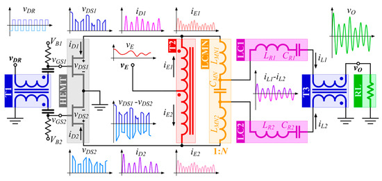
Figure 4.
Polar-mode Class-D HCVS PA diagram and waveforms.
- The envelope-input-related currents (iE1 and iE2) flowing in opposite directions in T2 windings result in magnetic flux cancellation, which provides an almost noninductive wideband envelope input (vE) port. Only some small inductances related to T2 leakage and the circuit-board layout are present in this path;
- The drain-to-source voltages (vDS1 and vDS2) described are as follows:
These result in a differential voltage defined by the following expression:
which is scaled by the 1:N ratio of the LC matching network (LCMN) and filtered by the LC resonators (LC1 and LC2), yielding an output voltage that can be expressed as follows:
where the sC square signal harmonics of (1) were removed. It must be noted that the envelope input (vE)-independent term is cancelled, which confirms the desired envelope input (vE) rejection effect on the amplified output signal (vO).
To benefit from these advantages, the EA should be placed as close as possible to the envelope supply port of the RF PA to reduce any inductance.
It is also important to note that the use of GaN HEMTs at these frequencies would simplify the input network by reducing it to just an input balun (T1) and some power resistors located at the transistor gates to improve input return losses and device stability.
2.3. Class-D PA Design and Simulations
The search for the most appropriate active device is crucial to implement an RF PA. In this particular case, considering peak envelope power (PEP) POUT = 100 W and vE = 28 V (drain supply voltage), the GaN HEMT CGH40090PP from Wolfspeed is a good candidate for this application.
As GaN HEMTs can be considered almost ideal switching devices at VHF, the PEP proposed for this class-D HCVS PA demonstrator can be obtained from the following expression:
which derived from (8), where RL corresponds to the 50 Ω RF load impedance.
Considering (9), the required 1:N ratio for the LCMN is , which means an impedance conversion from RL (50 Ω) to 25 Ω. This results in values of CMN = 25 pF and LMN = 30 nH, as well as inductance, which is provided by two inductors in the proposed LCMN balance structure. To complete the design of the class-D RF PA, the inductance and capacitance values for the series resonant tanks LC1 (LR1 = 22 nH, CR1 = 68 pF) and LC2 (LR2 = 22 nH, CR2 = 68 pF) were derived from AWR simulations (starting from the corresponding values for a resonance frequency of fres = 128 MHz and a quality factor of ) to provide a flat output power response over the entire bandwidth, while the rest of the components were also tuned to achieve the desired amplifier performance.
To achieve broadband operation, a reactance compensation effect was used in the load network. A similar effect has already been extensively described in the wideband class-E PA literature [20,21,22], but in the case of the class-D PA, an impedance profile was chosen that keeps the admittance phase of the load network around zero degrees and its magnitude constant over the entire operating bandwidth.
The full simulation results with the current component values, including the modeled input and output coaxial cable (50 Ω) baluns, as well as the coaxial hybrid coupler (T2) and the HEMT (CGH40090PP) simulation model (provided by Wolfspeed), are shown in Figure 5. The result of these simulations shows the performance of the RF PA operating in class D, where the transistor acts as a switching device requiring at least 30 dBm (PIN) of RF continuous wave (CW) drive signal (vDR) at its input port. Another parameter to control is the bias operating point (VGS and IDQ) of the RF PA, which, in switchmode PAs, defines the duty cycle of the drain waveforms and affects the power efficiency.

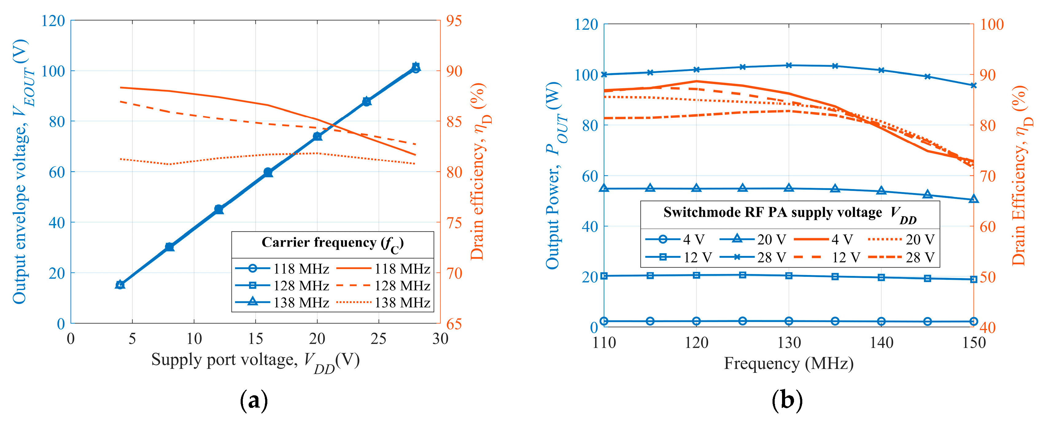
Figure 5.
Simulation results of the class-D PA (IDQ = 2 A and PIN = 1 W): (a) output envelope voltage and drain efficiency as a function of supply voltage and (b) output power flatness and drain efficiency performance in the operating frequency band.
2.4. Class-D PA Demonstrator Description
The class-D PA was implemented based on the simulations and principles described in the previous subsection. This implementation is based on transmission line transformers [23,24,25], and the transistor used is the CGHV40090PP GaN on silicon carbide (SiC) HEMT from the semiconductor manufacturer Wolfspeed that contains two cells closely located in one package, and, consequently, it is especially suitable for push–pull circuits (due to its low transistor-to-transistor inductance). This device is primarily intended for operation at higher frequencies than VHF, but it can be successfully operated at the VHF band because it does not contain any built-in matching networks, as long as it is properly stabilized. Its output equivalent capacitance is relatively low (CDS = 6 pF per transistor cell), which allows reasonable implementation of class D at the VHF band for the power levels and voltages involved in this circuit. This low-capacitance figure, combined with the low inductance provided by the hybrid coupler (T2), is the key factor that contributes to achieving a high cutoff frequency for the amplifier power supply injection port (vE). The hybrid coupler used in this amplifier is made of a 10 cm section of 25 Ω Polytetrafluoroethylene (PTFE) coaxial (not loaded with ferrite) cable. This hybrid and the output balun are connected by the following circuits:
- A symmetrical L-C matching network (LCMN) that is responsible for impedance transformation, consisting of a 28 pF total capacitance ATC 100B capacitors arrangement and two 40 mm sections of 25 Ω PTFE coaxial cable.
- Two (one per branch) low-Q resonators (LC1 and LC2) that provide both DC blocking and reactance compensation functions to ensure that wideband operation are made with a 28 μH Coilcraft inductor and a 68 pF ATC 100B capacitor each.
The output balun, which is responsible for providing a 25 Ω symmetrical impedance to each branch, consists of a 300 mm section of 50 Ω PTFE RG316 coaxial cable coiled (7 turns) on a 61-material ferrite core from Fair Rite.
The input circuit of this amplifier is made of a balun formed by a 300 mm section of RG178 50 Ω PTFE coaxial cable coiled (8 turns) on a 61-material toroidal core from Fair Rite. This balun is loaded at its output by four paralleled 100 Ohm SMD ¼ W thick film resistors (providing an approximately 25 Ω load) that are located across the transistor gates. These resistors are also used to stabilize the amplifier and to inject the negative DC voltage gate bias required by the transistor.
It is important to note that the power supply port (vE) to the output RF port (vO) isolation provided by this amplifier strongly depends on the effectiveness of the balanced-to-unbalanced performance and bandwidth of their baluns; consequently, they must be carefully designed and experimentally adjusted.
This prototype is built on a 0.8 mm thick FR4 two-sided laminate material with 1 oz. gold–nickel-plated copper layers. It is possible to use this inexpensive material for the amplifier PCB while keeping power losses low because most of the amplifier power is conducted by the coaxial cable transmission line transformers and circuit capacitors. This PCB assembly was mounted on an aluminum heatsink fitted with an embedded copper heat-spreader located below the transistor that is attached by means of screws. It did not require forced ventilation to operate at room temperature at full output power.
2.5. Class-D PA Demonstrator Measurements
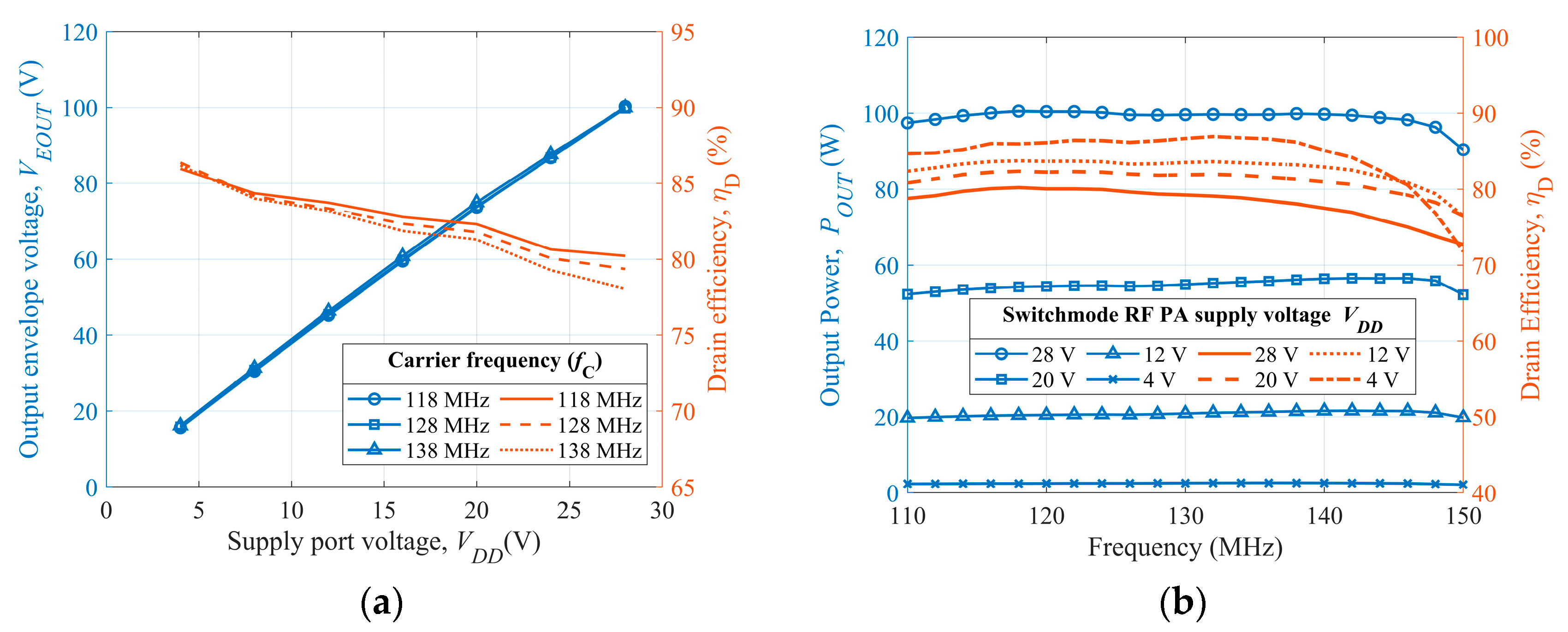
The power measurement results obtained from this amplifier are shown in Figure 6, and good agreement was found between the simulated and measured results. Figure 6 shows the measured output power (POUT) and drain efficiency (ηD) of the amplifier versus frequency at different power supply voltages (VDD) and driven by a PIN = 30 dBm input sinusoidal signal, exhibiting a very flat response within its operating bandwidth. For the same PIN, the static VDD-AM characteristic of the class-D PA is also shown, plotting the amplifier output voltage (VEOUT) as a function of the supply voltage (VDD), where good linearity is expected when the class-D RF PA is used as an AM high-level modulator. It is important to mention that, in these measurements, the static power supply signal referred to as VDD corresponds to the dynamic modulating signal referred to as vE in the other sections.
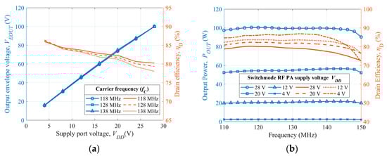
Figure 6.
Power measurements of the class-D PA prototype (IDQ = 2 A and PIN = 1 W): (a) output envelope voltage and drain efficiency as a function of supply voltage and (b) output power flatness and drain efficiency performance over the operating frequency band.
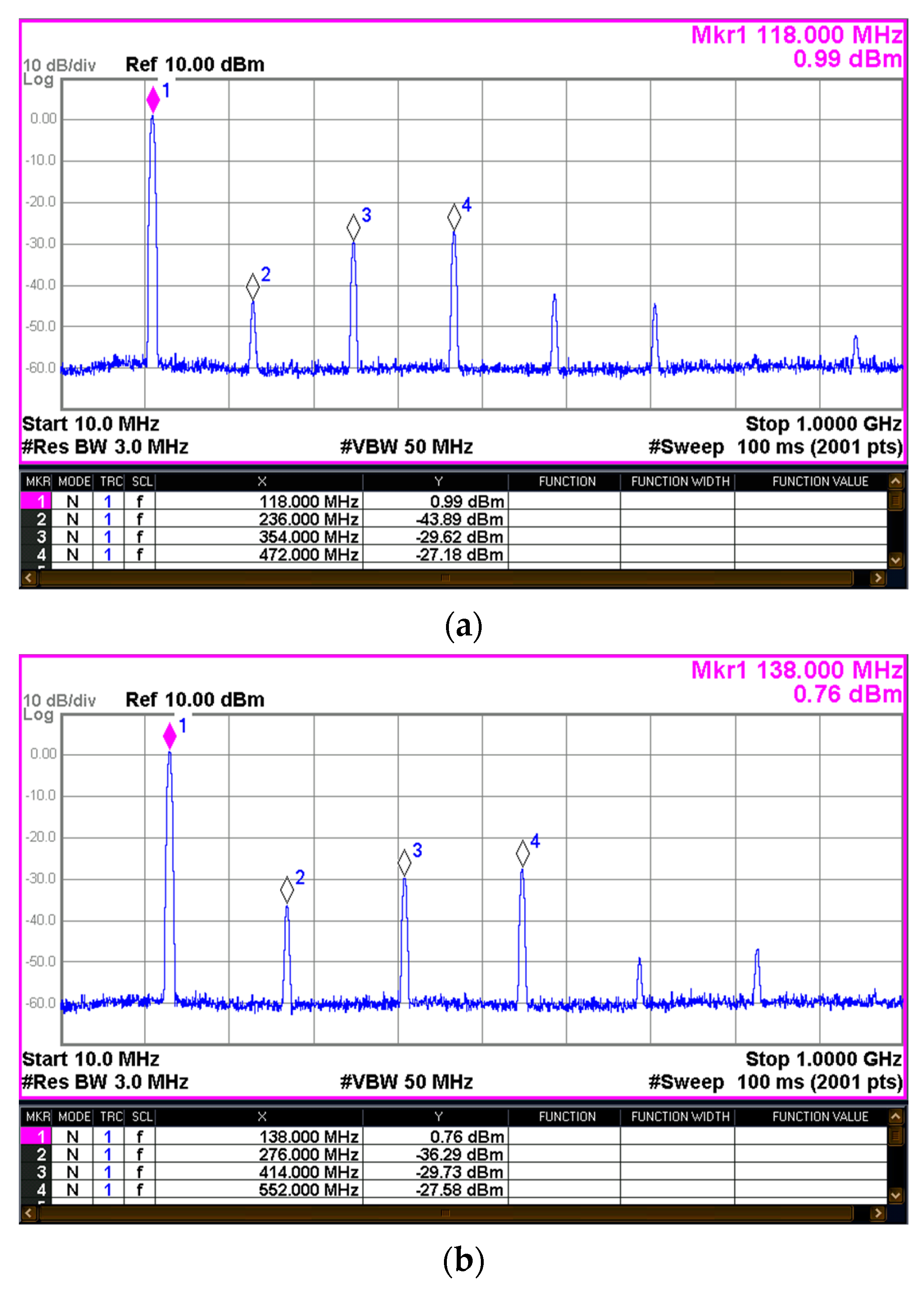
Figure 7 plots the spectral purity of the amplified signal when the amplifier is operating at its maximum output power and for the edges of its operating band.
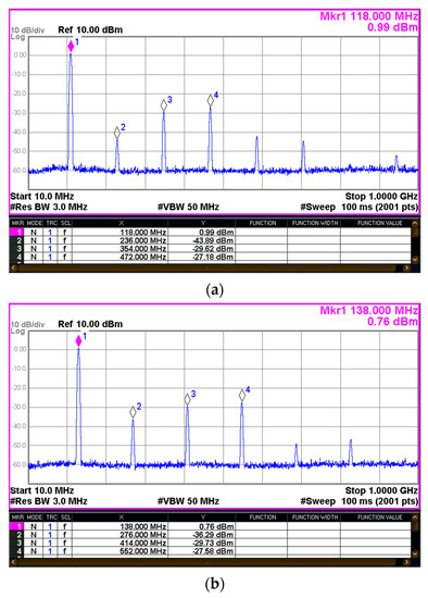
Figure 7.
Measured harmonic rejection of the class-D PA at 100 W output power (VDD = 28 V, IDQ = 2 A, and PIN = 1 W): (a) 118 MHz CW carrier and (b) 138 MHz CW carrier.
The measured harmonic rejection obtained by this amplifier, which uses no harmonic low-pass filter, is better than 35 dBc at 2fO harmonics within its operating bandwidth, and the rejection of all other harmonic content is better than 27 dBc. These results show a good balance of the push–pull structure, and, although it should be noted that the amplifier would need a harmonic rejection filter to meet the requirements of almost any communications service in this band, these measurements also serve to demonstrate that more than 99% of the RF power handled by the class-D RF PA is converted at its fundamental frequency component. Regarding the harmonics rejection required for a real transmitter, it can be said that, in view of the results obtained, it would be easy to meet harmonic rejection requirements ranging from 50 dBc to 60 dBc with a simple low-pass filter.
3. High-Efficiency Wideband Envelope Amplifier
One of the main fields of research when talking about polar transmitters or envelope elimination and restoration (EER) architectures is the EA, also sometimes known as a supply modulator. The main challenge presented by EAs is that they must provide enough bandwidth and a slew rate to meet the linearity needs of the envelope of the RF signal to be amplified (which can range from DC to tens of megahertz in some cases). Regarding this, the literature proposes a wide variety of design and implementation ideas [26,27,28,29,30], ranging from linear to switched to hybrid architectures. However, there are few commercial devices (operational amplifiers or DC-DC converters with a high dynamic response) that allow for the implementation of broadband EAs [31,32,33], and this portfolio is considerably reduced in regard to transmitters with high output power (>50 W) requirements. For this reason, although it was not the main goal of this work, it has been necessary to design and implement a wideband EA to verify the performance of the proposed class-D PA under wideband envelope modulation situations when integrated in a polar-mode transmitter. The proposed EA, which is shown in Figure 8, consists of a wideband linear EA (WLEA) powered by a switchmode slow envelope power supply (SEPS) to improve power efficiency.
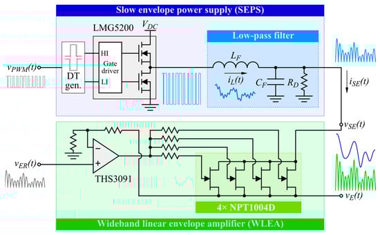
Figure 8.
Simplified diagram of the proposed EA circuit.
3.1. Wideband Linear Envelope Amplifier
To provide a WLEA with the required bandwidth for this application, an idea was proposed that should provide high slew rates and bandwidths, while being able to deliver a high output current. This is the use of RF HEMT GaN devices joined to operational amplifiers with high operating voltages and bandwidths in a DC-coupled common-drain arrangement. Specifically, this design uses the Texas Instruments THS3091 operational amplifier to drive four Macom NPT1004D GaN HEMTs connected in parallel.
The THS3091 combines high-speed (6000 V/µs) and wideband operation (305 MHz), with high output current drive capability (310 mA) from up to 32 V power supply. This allows the WLEA to operate in the supply voltage range required for the designed class-D VHF PA (0 V to 28 V), and its high slew rate and wideband operation together with its output current capability make it a reasonable choice for driving the equivalent gate capacitance (CGS) of the four paralleled GaN HEMTs. The 8-pin SOIC package with a thermal pad, in which this device is packaged, improves heat dissipation, which makes possible its operation at high frequencies when driving capacitive loads.
However, the main problem when using RF transistors in a common-drain linear power stage is their packaging, which is typically designed to provide heat dissipation through their source terminal, complicating the mechanical arrangement that satisfies both the common-drain scheme and the maintenance of a low-resistance thermal path. Accordingly, RF GaN transistors packaged in SOIC-8 have been preferred because of their small size and assembly flexibility. The chosen NPT1004D HEMTs can operate from DC to 4 GHz and have no integrated matching networks, making them ideal for this application.
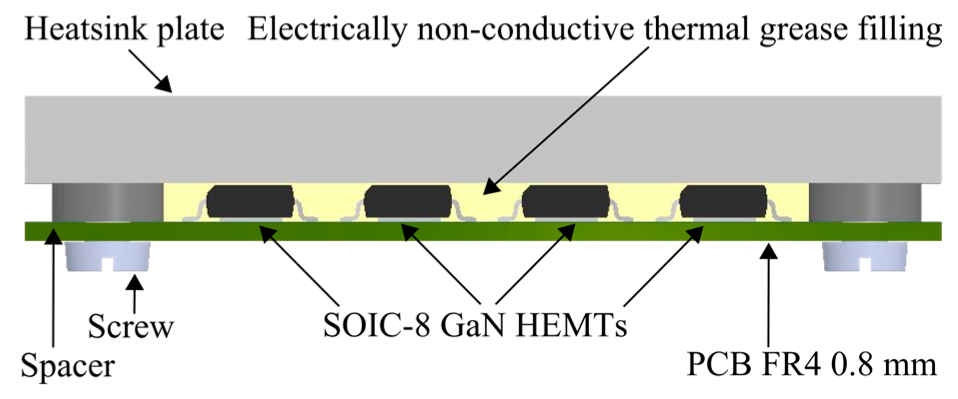
To remove the heat dissipated by these devices, the thermal pad intended for this purpose was not used, since it corresponds to the source of the transistor, which, in this case, is connected directly to the output of the EA, and doing so would complicate its mechanical assembly. For this reason, it was decided to capture the heat from the surface of the transistor package by means of a nonelectrically conductive thermal grease padding. This difficulty in removing heat from these devices has to do with the reason for using four transistors in parallel, which is to share the heat dissipated, allowing the transistors to operate within their temperature range. Simulations have been very helpful in determining the number of devices to parallel. Figure 9 shows the assembly diagram followed to achieve this. According to this assembly method, the WLEA prototype is built on a 0.8 mm double-sided FR4 printed circuit board to which an aluminum heatsink is attached.

Figure 9.
Assembly diagram for heat-sinking SOIC-8 GaN HEMTs through their packages.
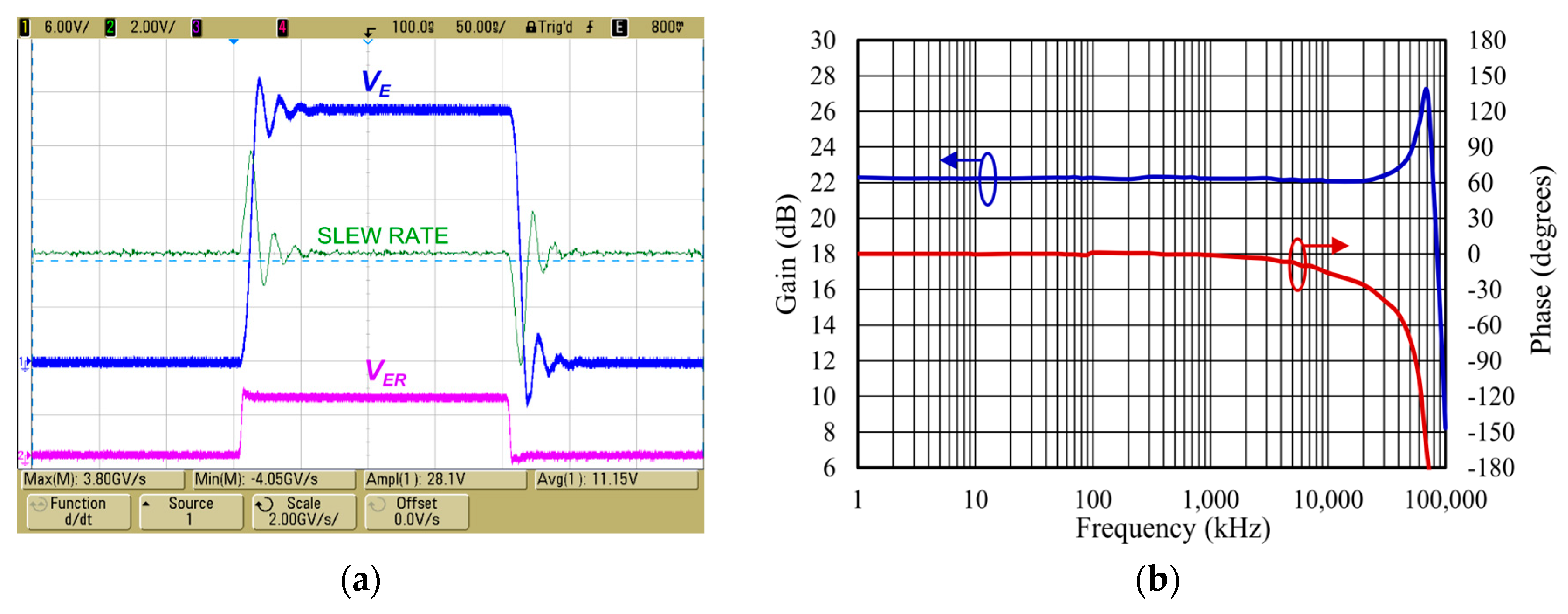
Some measurements were taken on this prototype to determine the performance this amplifier can provide for amplifying wideband envelope signals. To emulate the load that the class-D PA presents at its power port, a 6.8 Ω power resistor was used in parallel with a 470 pF ATC capacitor. Considering the results obtained in Figure 10, this WLEA has proven to be stable for a 28 V amplitude and 200 ns pulse, simultaneously providing a high slew rate and power bandwidth.
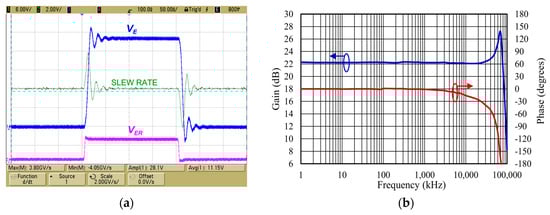
Figure 10.
Measured performance of the linear GaN HEMT based WLEA for a paralleled 6.8 Ω and 470 pF load: (a) output slew rate for a 200 ns pulse and (b) gain and phase frequency response. The red and blue circles and arrows indicate the y-axis to which the represented data belongs.
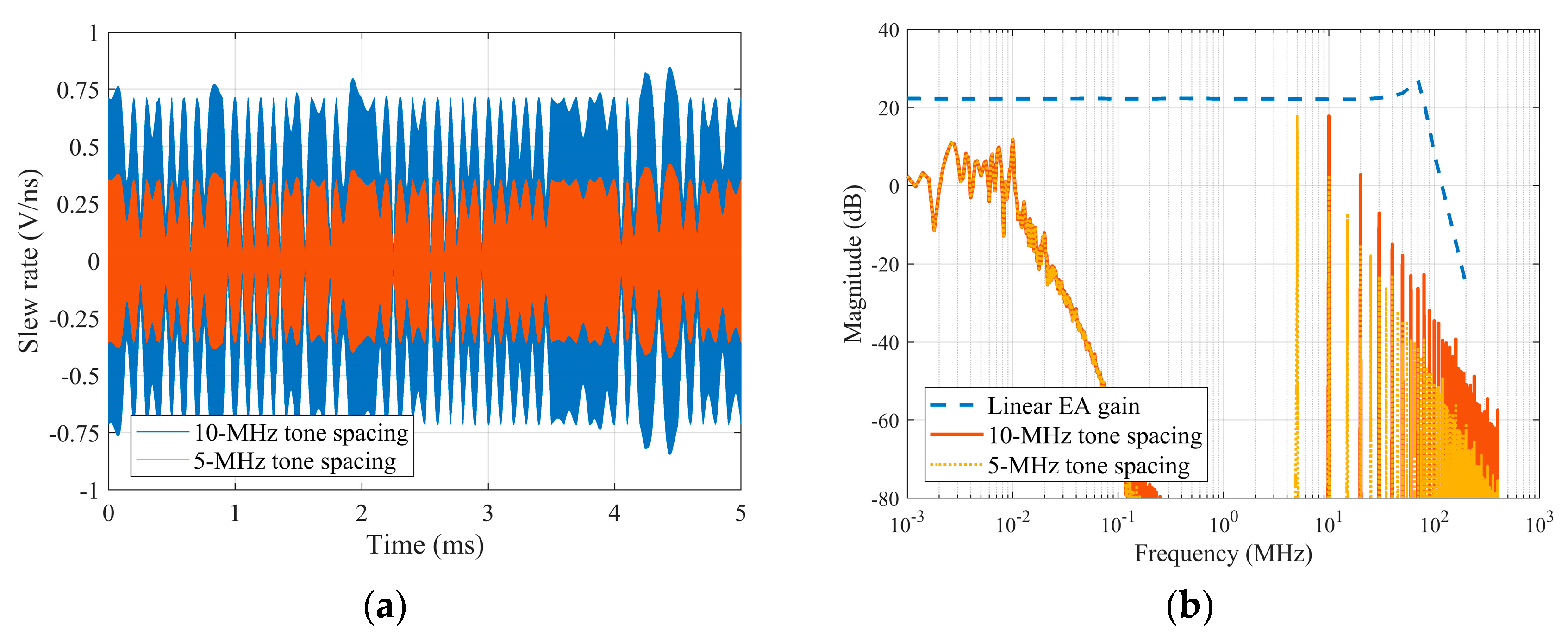
Figure 11 shows the required WLEA dynamic performance, where the slew rate of the envelope (vE) for a 2C-CH VDL-T signal, reaching a peak voltage of vEmax = 28 V for carrier spacings of 5 MHz and 10 MHz, can be observed. The test signal frequency representation shows how the components extend up to frequencies of tens of MHz, which leads to a high demand on the power bandwidth of the WLEA. An arbitrary signal generator (Agilent 81150A) controlled by a PC running MATLAB was used to support signal generation.
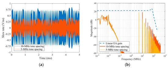
Figure 11.
Dynamic demands of the envelope of a 2C-CH VDL-T signal: (a) time-domain slew rate envelope requirements and (b) distribution of envelope frequency components compared with the gain of the linear EA.
In view of these data and compared with the graphs in Figure 10, it seems optimistic to think that the implemented WLEA can cover the linearity needs of a multicarrier system with up to a 10 MHz bandwidth.
3.2. Slow Envelope Power Supply
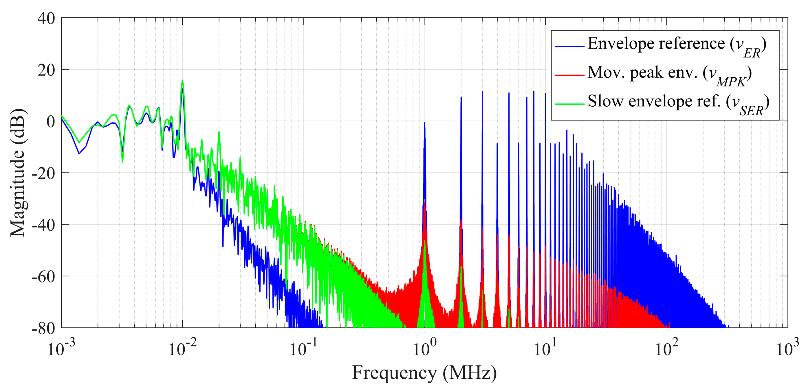
The WLEA presents good stability in frequency and draws good linearity figures. However, polar transmission techniques are supposed to improve the power efficiency of conventional RF PAs, and a linear amplifier may not be competitive to provide an improvement in these terms. To improve the efficiency of high-dynamic-performance linear regulators, several solutions (most of them based on a series combination because parallel topologies usually require a push–pull linear PA) have already been proposed for many years (slow ET, multilevel-based supply class-G PAs), and the common idea of all of them is usually to use a power supply that, in combination with the WLEA, is able to provide a variable voltage that tracks the amplified waveform [34,35,36,37,38]. As the WLEA is responsible for dynamic performance and linearity, the voltage tracking power supply does not have such stringent linearity and voltage ripple requirements, making it easy to implement, so conventional high-efficiency power conversion methods can be easily applied. For the generation of the slow envelope signal, there are several solutions described in the literature [39,40,41] that allow for real-time processing. However, in this case, we have used a method that allows this signal to be easily implemented in MATLAB. This process required two steps: The first one generated a signal called moving peak, vEMP, by using the movmax(A,k) MATLAB function over the envelope reference (vER) signal, with a sample frequency of fS = 800 MHz, using a number of points for the sliding window of k = 1000. The resulting signal was then passed through a moving mean filter function, movmean(A,k), to obtain a smoothing slow envelope reference (vSER) signal (with k = 1000) from which the digital pulse-width modulation (DPWM) control signal (vPWM) was generated, downsampled, and transferred to the arbitrary waveform generator (Agilent 81150A). Figure 12 shows the transformation of the envelope spectrum of a 4C-CH VDL-T (located at 120 MHz, 123 MHz, 128 MHz, and 130 MHz) signal through this process.
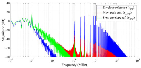
Figure 12.
Spectra of the envelope of a 4C-CH VDL-T (located at 120 MHz, 123 MHz, 128 MHz, and 130 MHz) signal. Reference envelope (vER), bandwidth-reduced envelope through a moving peak process (vMPK), and slow envelope resulting (vSER) from smoothing vMPK using a moving mean filter.
The design of this SEPS is based on [34,35] but adjusted to the wider bandwidth and higher power requirements of the test signals used in this work. In this case, the SEPS, consists of a half-bridge synchronous power cell controlled by the DPWM-generated signal (vPWM), followed by a low-pass L-C filter. The Texas Instruments LMG5200 eval board was used to implement the proposed SEPS. The LMG5200 IC is an 80 V, 10 A GaN half-bridge power stage with integrated drivers. The evaluation board also contains the dead-time generation circuitry and has a place reserved for the L-C low-pass output filter.
The design of this filter has been adapted to the needs of the envelope signals that have been used to test this polar-mode transmitter in order to demonstrate the potential performance improvement (in terms of power efficiency and linearity) that can be achieved by these systems. To demonstrate the broadband linearity performance of this system, some RF tests were conducted where several modulated narrowband signals were spaced at a minimum of 1 MHz within a 10 MHz bandwidth. This means that the L-C filter should offer a flat passband response over the slow envelope (vSE) bandwidth, while the output impedance at high frequencies should be kept low in order to supply the high-frequency current components (iSE) to the load.
To meet these specifications, an LF = 2.2 µH inductor and CF = 350 nF capacitor were selected for the filter. This results in a resonant frequency of fres = 200 kHz (one-tenth of the switching frequency, fsw) and provides 40 dB attenuation at the SEPS switching frequency (fsw = 2 MHz). Figure 13 shows the L-C low-pass filter response, together with the spectra of the vPWM control signal. It provides a flat amplitude response within the bandwidth of the slow envelope (vSER), while switching frequency components are attenuated and the output capacitor, CF, provides the high-frequency current components (iSE) of the filter output slow envelope signal (vSE).
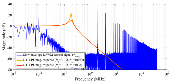
Figure 13.
SEPS slow envelope DPWM (vPWM) control signal spectra for the envelope of the 4C-CH VDL-T signal together with the frequency response of the SEPS low-pass filter magnitude.
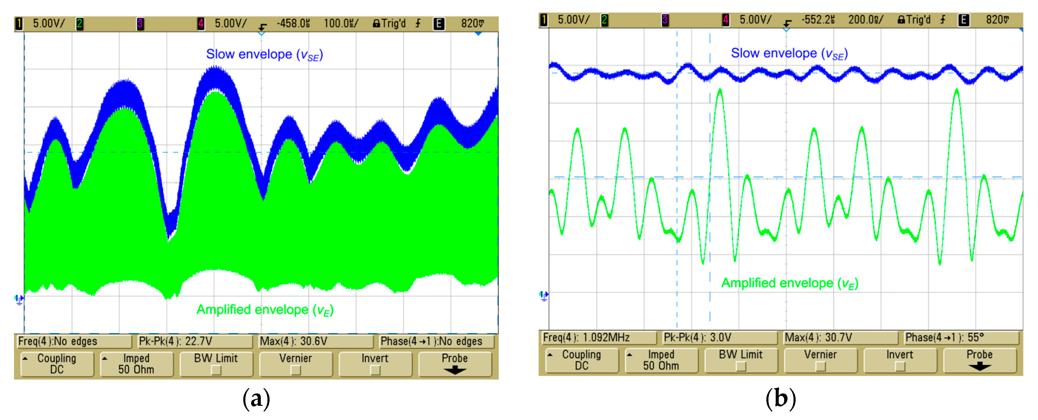
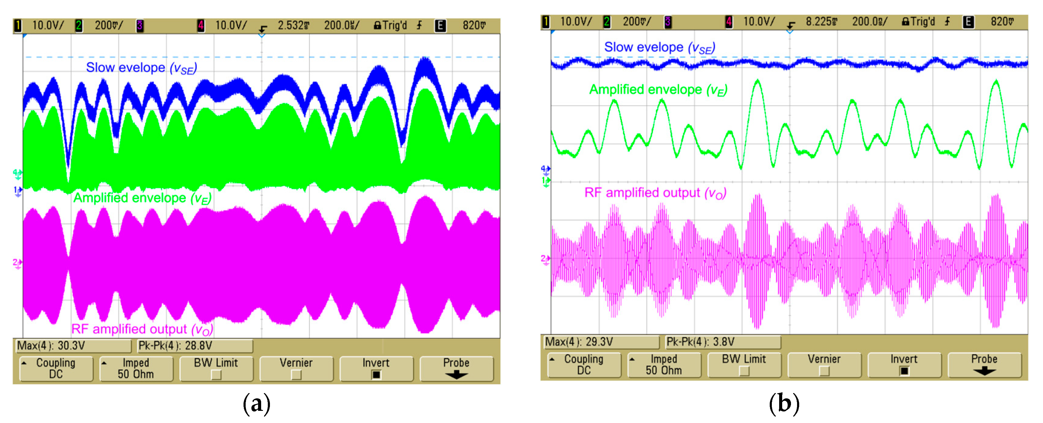
A signal corresponding to the envelope of a 4C-CH VDL-T signal was used to test the SEPS in combination with the WLEA. The time-domain output voltage waveforms are shown in Figure 14 for a peak power of PEOPK = 125 W and a mean power of PEO = 24 W (PAPR = 7.2 dB) from a main supply voltage of VS = 34 V. The voltage ripple at the SEPS output (vSE) is due to the strong high-frequency iSE currents and the impedance presented by the output L-C filter capacitor, CF, at these frequencies, but these nonlinearities are filtered out by the WLEA and do not affect the linearity of its output (vE), as seen in Figure 14b.
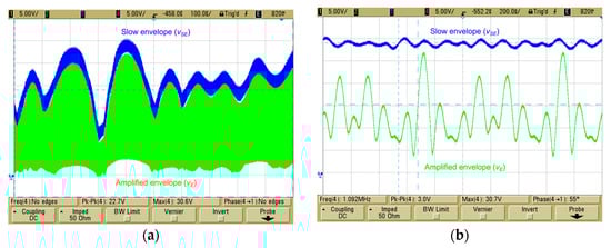
Figure 14.
Time-domain measured EA output (vSE) and SEPS output (vE) for the envelope of the 4C-CH VDL-T signal at 125 W peak output power: (a) envelope waveforms (vSE and vE) and (b) detail of the EA output (vE) waveform.
For hybrid EAs (regardless of whether they are made up of serial or parallel combinations of linear and switchmode power stages), the power efficiency depends on the bandwidth of the envelope signal: the wider the bandwidth is, the lower the efficiency. This is because the switching amplifier (SEPS in this case) can only cover the low-frequency components, and, particularly in this case, this effect is noticeable due to the large amount of energy of the high-frequency envelope components (as seen in the PSD plotted in Figure 12), which are totally dependent on being amplified by the WLEA. Therefore, although the SEPS provides very high power efficiency (over 90%), the overall efficiency of the EA remains around ηEA = 52% (for the envelope of the wideband 4C-CH VDL-T test signal), which, although at first glance may seem to be a discreet value, is quite a satisfactory figure considering the demanding nature of the envelope (vE) of the test signal (which has a PAPR = 7.23 dB) in terms of its bandwidth and spectral distribution.
4. Polar-Mode Wideband VHF PA Demonstrator Results
The combination of the SEPS, WLEA, and VHF class-D PA was carried out, as shown in Figure 15, where all the implemented circuits can be seen, and their main elements are identified. In this assembly, special attention was paid to the connection between the output of the WLEA and the power port of the class-D PA. This should be as short as possible, since large bandwidth signals are handled by these circuits, and the increase in inductance at this point may contribute to a deformation of the amplified envelope waveform.
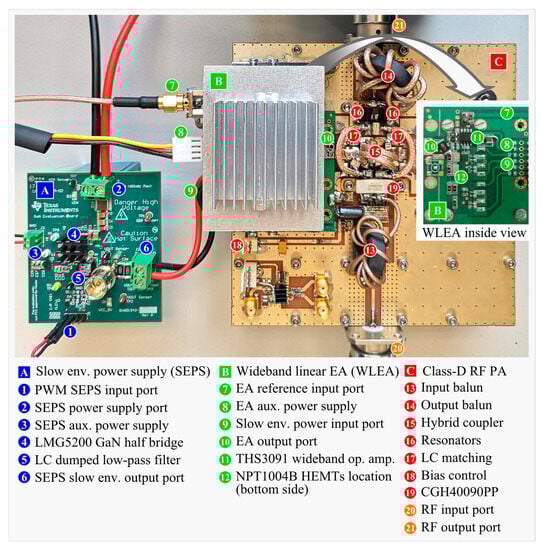
Figure 15.
Demonstrator circuit of the SEPS, WLEA and class-D VHF PA polar-mode assembly.
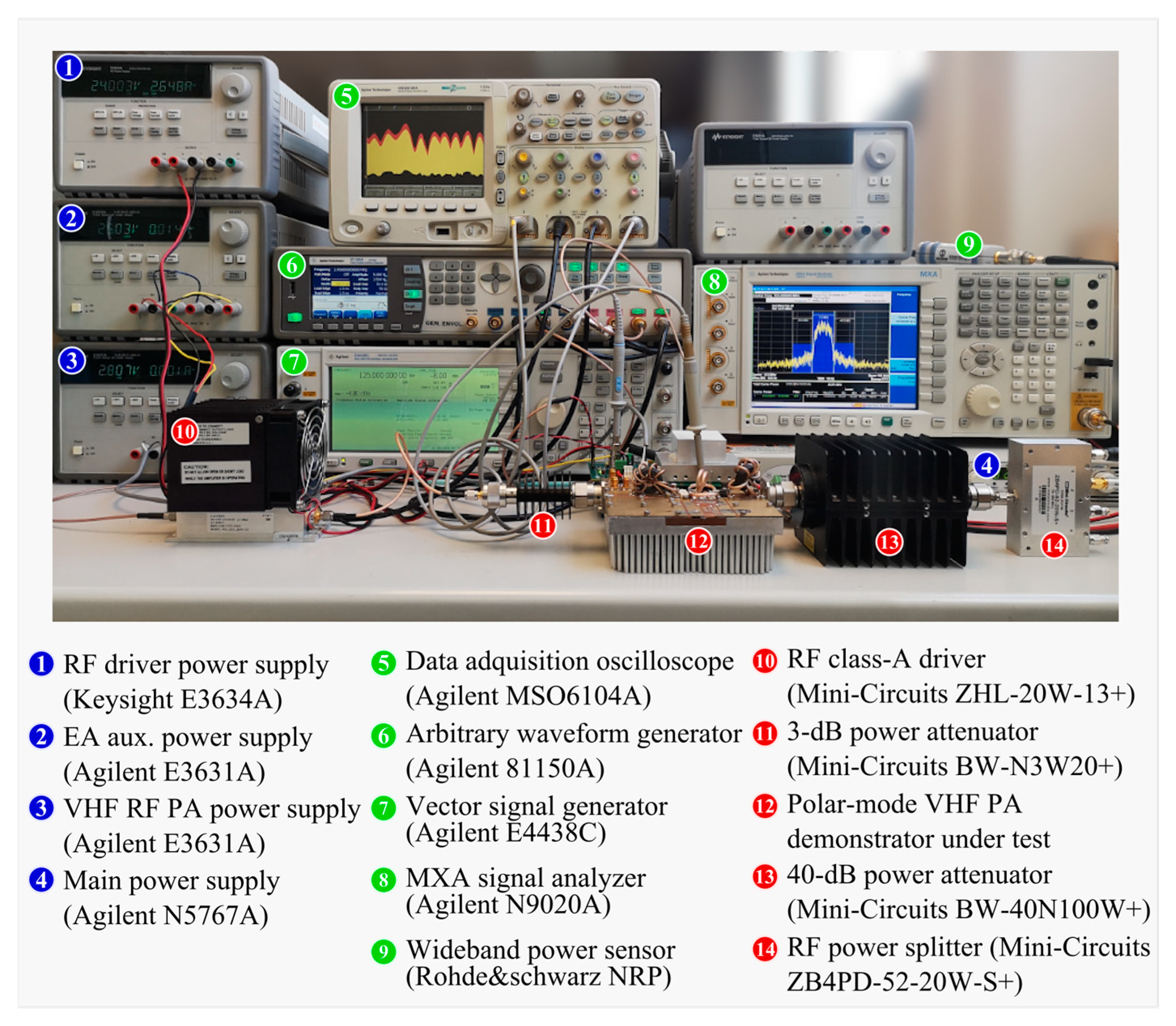
To verify the viability of the polar amplification system developed in this work, the test bench shown in Figure 16 was employed. All the test and measurement instruments used are described in Figure 16, and a PC running MATLAB was used for the control of these instruments and for the generation, capture, and processing of the signals used in the tests that were carried out. These measurements include tests of multicarrier signals with analog and digital modulations. The signals were generated using MATLAB, and the constant envelope-phase modulated signal was loaded into the vector signal generator (Agilent E4438C), using a sampling rate of fs = 100 MHz, while the envelope signal and the PWM of the slow envelope were transferred to the arbitrary waveform generator (Agilent 81150A), with a resulting sampling frequency of approximately fs = 50 MHz.
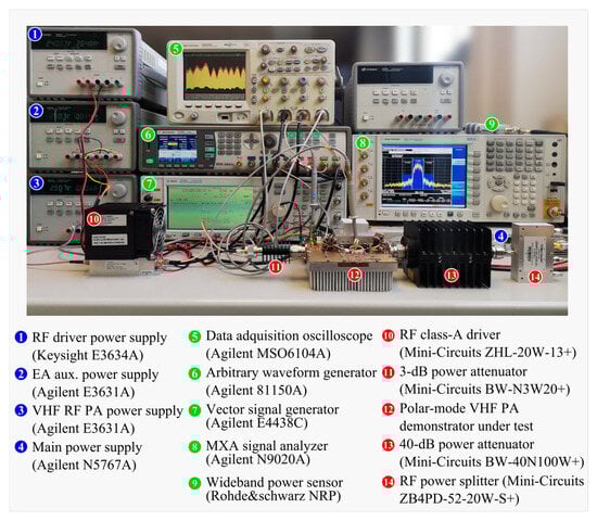
Figure 16.
Test bench used to take the measurements of the implemented polar-mode VHF PA demonstrator.
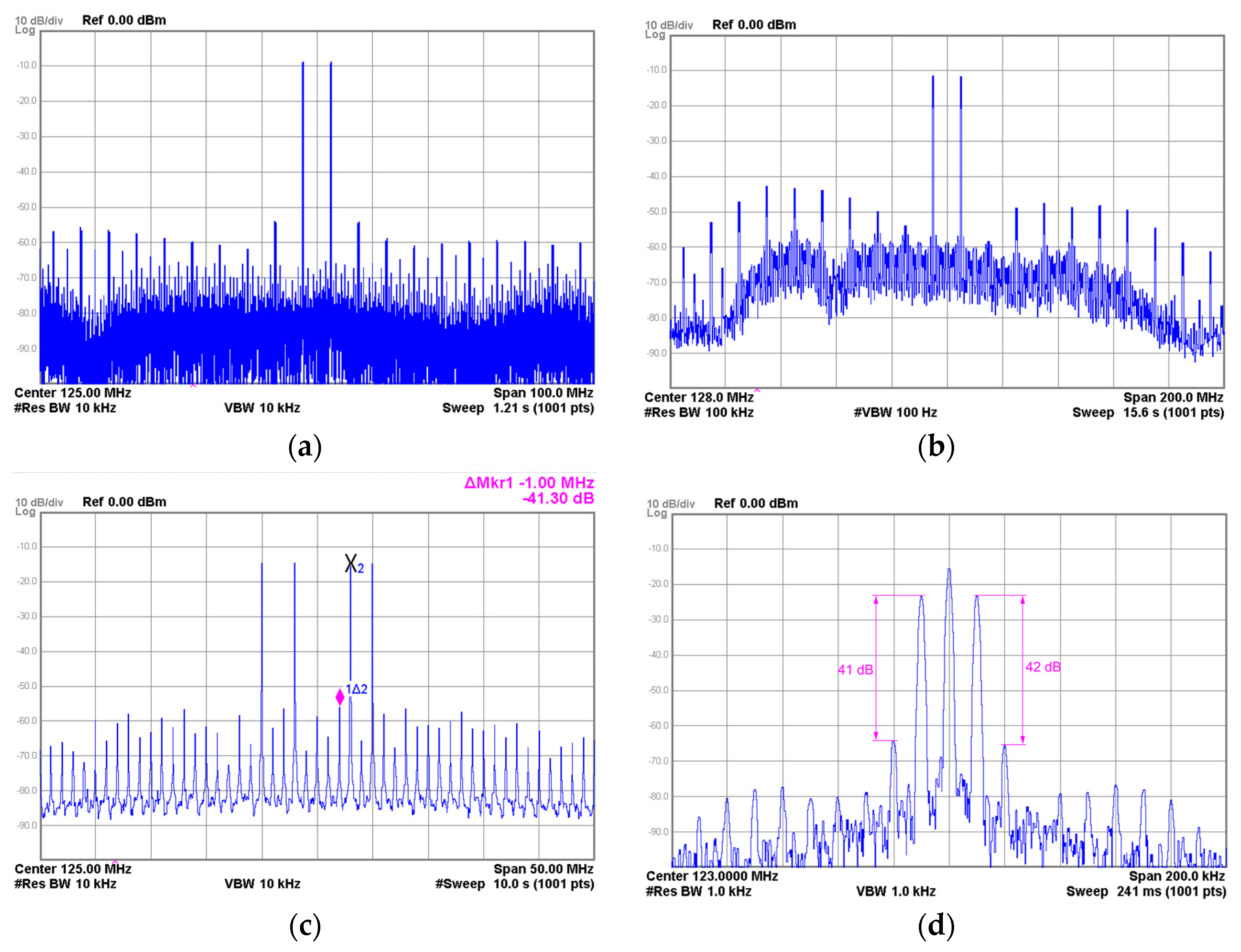
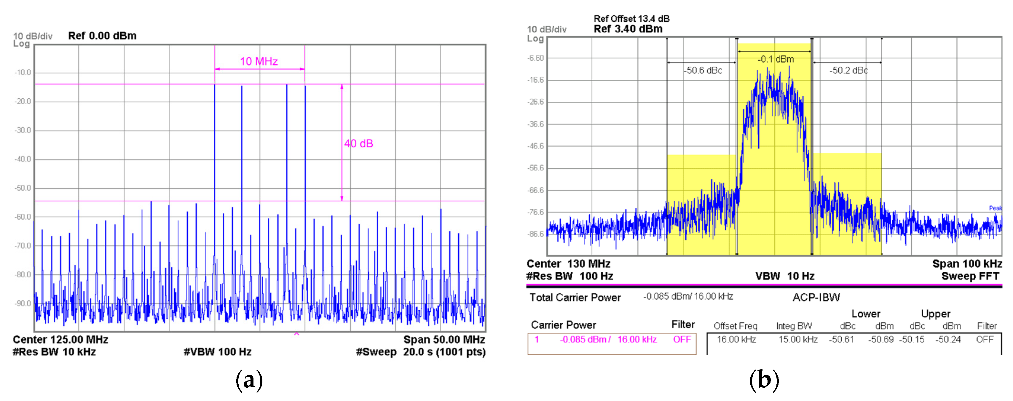
In the first case, the results shown in Figure 17a correspond to the 2C-CH AM-T signal with a carrier spacing of 5 MHz (at 125 MHz center frequency). In the second test, the carriers of the 2C-CH AM-T signal were separated up to 10 MHz to determine the limits of the demonstrator, as shown in Figure 17b. The AM test ends with a 4C-CH AM-T signal (located at 120 MHz, 123 MHz, 128 MHz, and 130 MHz), which can be seen in Figure 17c. This test covers a total bandwidth of 10 MHz, with more than 40 dB of attenuation for the unwanted spectral components, and presents good linearity figures for each individual channel, as seen in the detail of one of the channels shown in Figure 17d. The main supply voltage used to take these measurements was VS = 34 V, the peak output power reached POUT = 94 W PEP, and the resulting overall power efficiency was ηO = 47%. This can be considered a satisfactory figure considering that the signal used in the test has a PAPR = 6.5 dB and taking into account the PSD of the signal envelope.

Figure 17.
Spectral measurements of AM-T multicarrier signals at the output of the polar-mode PA at 94 W peak output power (RF PA IQ = 2 A; and main supply voltage, VS = 34 V): (a) 2C-CH AM-T signal 5 MHz carrier spacing, (b) 2C-CH AM-T signal 10 MHz carrier spacing, (c) 4C-CH AM-T signal 10 MHz bandwidth, and (d) detail of the 123 MHz channel.
The second set of measurements was carried out using the 4C-CH VDL-T signal (located at 120 MHz, 123 MHz, 128 MHz, and 130 MHz). The metrics used to determine the performance that can be obtained in this case, were the adjacent channel power ratio (ACPR) and error vector magnitude (EVM) for each channel, the measurement of spurious in the operating band, and the total power efficiency of the polar amplifier. Figure 18 shows the most relevant output time-domain waveforms obtained with an oscilloscope, and Figure 19 shows some of the spectra collected during the measurement process. A summary of all the data obtained and processed is shown in Table 1. It is important to note that the linearity and performance figures shown in Table 1 were achieved without the need for additional linearization techniques, such as digital predistortion (DPD). In this table, in addition to the individual linearity and output power measurements for each channel (EVM and ACPR), the total polar-mode PA power efficiency and power-added efficiency (PAE) computations are also shown.

Figure 18.
Time-domain measurements of an amplified 95 W peak output power 4C-CH VDL-T signal (located at 120 MHz, 123 MHz, 128 MHz, and 130 MHz) at the output of the polar-mode PA (RF PA IDQ = 2 A; main supply voltage, VS = 34 V): (a) envelope (vSE, vE) and RF (vO) output waveforms; and (b) detail of the amplified envelope (vE) and RF (vO) output waveforms.

Figure 19.
Spectral measurements of an amplified 95 W peak output power 4C-CH VDL-T signal (located at 120 MHz, 123 MHz, 128 MHz, and 130 MHz) at the output of the polar-mode PA (RF PA IDQ = 2 A; main supply voltage, VS = 34 V): (a) IMD and spurious frequency attenuation; and (b) detail of the 130 MHz channel ACPR measurements.

Table 1.
Summary of P-RFPA linearity and power performance for a 4C-CH VDL-T signal.
5. Discussion
The use of GaN HEMT power semiconductor devices at VHF is unusual, as the latest Si-LDMOS devices at these frequencies can provide very good results in terms of power efficiency at a lower cost. Therefore, there is a scarcity of published scientific works based on GaN technology at these frequency bands, and it is difficult to find published results to compare with those obtained in this work because most of the developments are currently focused on the higher-frequency bands (above UHF) and ET PA architectures [42,43,44]. However, there are new communication services, such as the one addressed in this work (satellite communications at the VHF band), that are currently under development and can benefit from using GaN technology in RF power circuits. Regardless of the carrier frequency used, GaN HEMTs (which exhibit lower parasitic elements compared to those of Si-LDMOS devices) can provide a better performance in wide fractional bandwidth PAs, while maintaining good linearity figures, resulting in an increase in power efficiency, as already demonstrated by some broadband PAs operating in this band [45]. These linearity and power efficiency features can be enhanced if a polar-mode architecture is used in such a way that the RF GaN PA is combined with a wideband EA whose power stages have also been developed with GaN technology, as described in this paper.
In view of the polar-mode PA performance results, it seems reasonable to compare this type of amplification architecture (which seems to be more complex at the hardware level) with Doherty PAs [46,47]. However, although the power efficiency of Doherty PAs (for which there are no previously published results or similar works for a direct comparison) may be at levels close to those obtained by the polar-mode system developed in this study, it must be taken into consideration that to reach the linearity levels of the polar-mode transmitter, the Doherty topology would need to use complementary linearization techniques, such as wideband digital predistortion [48,49,50,51,52,53], which, in addition to requiring additional hardware to digitalize the amplified output signals, requires complex adaptive digital processing hardware capable of operating in real time. It is also important to mention other techniques, such as Chireix [54], that allow users to obtain high-power-efficiency figures, but given the high fractional bandwidth that would be necessary in the combiner, as well as the control techniques required, it seems complicated to use it for this application.
Therefore, these initial results suggest that the proposed full GaN-based polar-mode PA demonstrator shown in this paper, which still has room for improvement and optimization, could be an attractive alternative to consider for the implementation of PAs for this type of application.
6. Conclusions
This work is motivated by the newly emerging multicarrier satellite communication services at the VHF band that require linear and power-efficient PAs in their transmitters. Therefore, a solution to reduce envelope distortion in high efficiency and wide fractional bandwidth polar-mode PAs was described and tested to meet the demands of the satellite transmitters used in this application. Additionally, a hybrid EA (linear and switchmode power stages combination) that was also based on GaN HEMT technology was developed to verify the functionality of the system.
The demonstrator for the VHF HCVS class-D PA operating in polar mode in combination with the proposed EA was tested for wide fractional bandwidth multicarrier analog and digitally modulated signals, yielding good linearity and power efficiency figures. This shows that the proposed idea of using a GaN-based HCVS class-D topology for RF PA design is a feasible way to mitigate the nonlinearity issues concerning these polar-mode PA architectures when high-performance EAs (also built with GaN devices) are used for modulating its power supply port. Furthermore, these results show that the proposed system did not require the use of DPD techniques, as other PA architectures (e.g., Doherty PAs) usually do, considering the overall power efficiency and the demanding linearity nature of the modulated multicarrier signal envelope.
Author Contributions
Conceptualization, M.P.-G. and F.-J.O.-G.; methodology, M.P.-G.; software, M.P.-G.; validation, M.P.-G. and F.-J.O.-G.; formal analysis, M.P.-G. and F.-J.O.-G.; resources, F.-J.O.-G.; writing—original draft preparation, M.P.-G.; writing—review and editing, M.P.-G. and F.-J.O.-G.; supervision, F.-J.O.-G.; project administration, F.-J.O.-G. All authors have read and agreed to the published version of the manuscript.
Funding
This research received no external funding.
Data Availability Statement
Not applicable.
Conflicts of Interest
The authors declare no conflict of interest.
References
- Cripps, S.C. RF Power Amplifiers for Wireless Communication, 3rd ed.; Artech House: Norwood, MA, USA, 1999. [Google Scholar]
- Singh, S.; Malik, J. Review of efficiency enhancement techniques and linearization techniques for power amplifier. Int. J. Circ. Theor. Appl. 2021, 49, 762–777. [Google Scholar] [CrossRef]
- Kahn, L.R. Single sideband transmission by envelope elimination and restoration. Proc. Inst. Radio Eng. 1952, 40, 803–806. [Google Scholar] [CrossRef]
- Raab, F.H.; Rupp, D.J. High-efficiency single-sideband HF/VHF transmitter based upon envelope elimination and restoration. In Proceedings of the 1994 Sixth International Conference on HF Radio Systems and Techniques, York, UK, 4–7 July 1994; pp. 21–25. [Google Scholar] [CrossRef]
- McCune, E. Operating Modes of Dynamic Power Supply Transmitter Amplifiers. IEEE Trans. Microw. Theory Tech. 2014, 62, 2511–2517. [Google Scholar] [CrossRef]
- McCune, E. Dynamic Power Supply Transmitters: Envelope Tracking, Direct Polar, and Hybrid Combinations; Cambridge University Press: Cambridge, UK, 2015. [Google Scholar]
- McCune, E. A Technical Foundation for RF CMOS Power Amplifiers: Part 6: Relating Envelope Tracking and Polar PA Operation. IEEE Solid-State Circuits Mag. 2016, 8, 74–80. [Google Scholar] [CrossRef]
- Asbeck, P.; Popovic, Z. ET Comes of Age: Envelope Tracking for Higher-Efficiency Power Amplifiers. IEEE Microw. Mag. 2016, 17, 16–25. [Google Scholar] [CrossRef]
- Popovic, Z. Amping Up the PA for 5G: Efficient GaN Power Amplifiers with Dynamic Supplies. IEEE Microw. Mag. 2017, 18, 137–149. [Google Scholar] [CrossRef]
- Raab, F. Drive modulation in kahn-technique transmitters. Microw. Symp. Dig. IEEE MTT-S Int. 1999, 2, 811–814. [Google Scholar] [CrossRef]
- Baxandall, P.J. Transistor Sine Wave LC Oscillators, Some General Considerations and New Developments. IEE Proc. Electric. Power Appl. 1959, 106, 748–758. [Google Scholar] [CrossRef]
- Krauss, H.L.; Bostian, C.W.; Raab, F.H. Solid State Radio Engineering, 2nd ed.; John Wiley & Sons: Hoboken, NJ, USA, 2003. [Google Scholar]
- Grebennikov, A.; Sokal, N.O.; Franco, M.J. Switchmode RF and Microwave Power Amplifiers, 2nd ed.; Academic Press: Cambridge, MA, USA, 2012. [Google Scholar]
- Kazimierczuk, M.K. Class D voltage-switching MOSFET power amplifier. IEE Proc. B (Electr. Power Appl.) 1991, 138, 285–296. [Google Scholar] [CrossRef]
- Oyane, A.; Senanayake, T.; Hattori, F.; Imaoka, J.; Yamamoto, M.; Masuda, M. 13.56MHz High Power Half-Bridge GaN-HEMT Resonant Inverter Achieving 99% Power Efficiency. In Proceedings of the IEEE International Conference on Power Electronics, Drives and Energy Systems (PEDES), Jaipur, India, 16–19 December 2020; pp. 1–4. [Google Scholar] [CrossRef]
- Kobayashi, H.; Hinrichs, J.M.; Asbeck, P.M. Current-mode class-D power amplifiers for high-efficiency RF applications. IEEE Trans. Microw. Theory Tech. 2001, 49, 2480–2485. [Google Scholar] [CrossRef]
- Zhang, Z.; Nghiem, X.A.; Negra, R.; Boeck, G. 1 kW 13.56 MHz Class-D−1 Power Stage with 90 % Drain Efficiency. In Proceedings of the 12th German Microwave Conference (GeMiC), Stuttgart, Germany, 25–27 March 2019; pp. 252–255. [Google Scholar] [CrossRef]
- Raab, F.H. Get broadband, dual-mode operation with this FET power amplifier. EDN Mag.-Electr. Des. News 1978, 23, 117–124. [Google Scholar]
- Raab, F.H.; Rupp, D.J. HF power amplifier operates in both class B and class D. In Proceedings of the RF Expo West, San Jose, CA, USA, 17–19 March 1993; pp. 114–124. [Google Scholar]
- Everard, J.K.A.; King, A.J. Broadband power efficient Class E amplifiers with a non-linear CAD model of the active MOS device. J. IERE 1987, 57, 52–58. [Google Scholar] [CrossRef]
- Grebennikov, A. Simple design equations for broadband class E power amplifiers with reactance compensation. In Proceedings of the IEEE MTT-S International Microwave Sympsoium Digest, Phoenix, AZ, USA, 20–24 May 2001; Volume 3, pp. 2143–2146. [Google Scholar] [CrossRef]
- Kumar, N.; Prakash, C.; Grebennikov, A.; Mediano, A. High-Efficiency Broadband Parallel-Circuit Class E RF Power Amplifier with Reactance-Compensation Technique. IEEE Trans. Microw. Theory Tech. 2008, 56, 604–612. [Google Scholar] [CrossRef]
- Blocksome, R.K. Practical Wideband RF Power Transformers, Combiners and Splitters. In Proceedings of the RF Technology Expo 86, Anaheim, CA, USA, 30 January–1 February 1986; pp. 207–227. [Google Scholar]
- Sevick, J. Transmission Line Transformers, 4th ed.; SciTech Publishing: Raleigh, NC, USA, 2001. [Google Scholar]
- Grebennikov, A. Power combiners, impedance transformers and directional couplers. High Freq. Electron. 2007, 6, 20–38. [Google Scholar]
- Wang, Z. Envelope Tracking Power Amplifiers for Wireless Communications; Artech House: Norwood, MA, USA, 2014. [Google Scholar]
- Raab, F. Split-band modulator for Kahn-technique transmitters. IEEE MTT-S Int. Microw. Symp. Dig. 2004, 2, 887–890. [Google Scholar] [CrossRef]
- Ruan, X.; Wang, Y.; Jin, Q. A review of envelope tracking power supply for mobile communication systems. CPSS Trans. Power Electron. Appl. 2017, 2, 277–291. [Google Scholar] [CrossRef]
- Bhardwaj, S.; Moallemi, S.; Kitchen, J.A. Review of Hybrid Supply Modulators in CMOS Technologies for Envelope Tracking PAs. IEEE Trans. Power Electron. 2023, 38, 6036–6062. [Google Scholar] [CrossRef]
- García, O.; Vasić, M.; Alou, P.; Oliver, J.A.; Cobos, J.A. An Overview of Fast DC–DC Converters for Envelope Amplifier in RF Transmitters. IEEE Trans. Power Electron. 2013, 28, 4712–4722. [Google Scholar] [CrossRef]
- Analog Devices. High Speed, High Voltage, 1 A Output Drive Amplifier, ADA4870 Datasheet, Rev. A, August 2022. Available online: https://www.analog.com/media/en/technical-documentation/data-sheets/ada4870.pdf (accessed on 3 June 2023).
- Analog Devices. 1.1 A, 35 MHz Current, Feedback Amplifier. LT1210 Datasheet, Rev. C, April 2018. Available online: https://www.analog.com/media/en/technical-documentation/data-sheets/lt1210.pdf (accessed on 3 June 2023).
- Apex Microtechnology. Power Operational Amplifiers. PA107DP Datasheet, Rev. J, January 2020. Available online: https://www.apexanalog.com/resources/products/pa107u.pdf (accessed on 28 June 2023).
- Kitchen, J.; Chu, W.Y.; Deligoz, I.; Kiaei, S.; Bakkaloglu, B. Combined Linear and Δ-Modulated Switched-Mode PA Supply Modulator for Polar Transmitters. In Proceedings of the IEEE International Solid-State Circuits Conference Digest of Technical Papers, San Francisco, CA, USA, 11–15 February 2007; pp. 82–588. [Google Scholar] [CrossRef]
- Cheng, P.M.; García, O.; Vasić, M.; Alou, P.; Oliver, J.A.; Montoro, G.; Cobos, J.A. Envelope amplifier based on a hybrid series converter with the slow-envelope technique. In Proceedings of the IEEE Energy Conversion Congress and Exposition (ECCE), Raleigh, NC, USA, 15–20 September 2012; pp. 1–5. [Google Scholar] [CrossRef]
- Raab, F.H. Average Efficiency of Class-G Power Amplifiers. IEEE Trans. Consum. Electron. 1986, 2, 145–150. [Google Scholar] [CrossRef]
- Watkins, B.G. A High Bandwidth Class G Current-Mode Amplifier for Envelope Modulators. High Freq. Electron. 2011, 10, 20–24. [Google Scholar]
- Varlamov, O.; Nguyen, D.C.; Grebennikov, A. Broadband and Efficient Envelope Amplifier for Envelope Elimination and Restoration/Envelope Tracking Higher-Efficiency Power Amplifiers. Sensors 2022, 22, 9173. [Google Scholar] [CrossRef] [PubMed]
- Montoro, G.; Gilabert, P.; Bertran, E.; Berenguer, J. A method for real-time generation of slew-rate limited envelopes in envelope tracking transmitters. In Proceedings of the IEEE International Microwave Workshop Series on RF Front-Ends for Software Defined and Cognitive Radio Solutions (IMWS), Aveiro, Portugal, 22–23 February 2010; pp. 1–4. [Google Scholar] [CrossRef]
- Jeong, J.; Kimball, D.F.; Kwak, M.; Hsia, C.; Draxler, P.; Asbeck, P.M. Wideband Envelope Tracking Power Amplifiers with Reduced Bandwidth Power Supply Waveforms and Adaptive Digital Predistortion Techniques. IEEE Trans. Microw. Theory Tech. 2009, 57, 3307–3314. [Google Scholar] [CrossRef]
- Gilabert, P.L.; Montoro, G. Look-Up Table Implementation of a Slow Envelope Dependent Digital Predistorter for Envelope Tracking Power Amplifiers. IEEE Microw. Wirel. Compon. Lett. 2012, 22, 97–99. [Google Scholar] [CrossRef]
- Kwan, A.K.; Younes, M.; Darraji, R.; Ghannouchi, F.M. On Track for Efficiency: Concurrent Multiband Envelope-Tracking Power Amplifiers. IEEE Microw. Mag. 2016, 17, 46–59. [Google Scholar] [CrossRef]
- Yan, J.J.; Cowles, D.E.; Kimball, D.; Mattsson, A. Multi-Carrier Envelope Tracking Power Amplifier. In Proceedings of the IEEE Military Communications Conference (MILCOM), Los Angeles, CA, USA, 29–31 October 2018; pp. 313–316. [Google Scholar] [CrossRef]
- Hamid, S.S.; Mariappan, S.; Rajendran, J.; Rawat, A.S.; Rhaffor, N.A.; Kumar, N.; Nathan, A.; Yarman, B.S. A State-of-the-Art Review on CMOS Radio Frequency Power Amplifiers for Wireless Communication Systems. Micromachines 2023, 14, 1551. [Google Scholar] [CrossRef]
- Mini-Circuits. High Power Amplifier. ZHL-50W-GAN + Datasheet, Rev. 0R. Available online: https://www.minicircuits.com/pdfs/ZHL-50W-GAN+.pdf (accessed on 30 July 2023).
- Doherty, W.H. A New High Efficiency Power Amplifier for Modulated Waves. Proc. IRE 1936, 24, 1163–1182. [Google Scholar] [CrossRef]
- Pengelly, R.; Fager, C.; Ozen, M. Doherty’s Legacy: A History of the Doherty Power Amplifier from 1936 to the Present Day. IEEE Microw. Mag. 2016, 17, 41–58. [Google Scholar] [CrossRef]
- Naskas, N.; Papananos, Y. Neural-network-based adaptive baseband predistortion method for RF power amplifiers. IEEE Trans. Circuits Syst. II Express Briefs 2004, 51, 619–623. [Google Scholar] [CrossRef]
- Woo, Y.Y.; Kim, J.; Yi, J.; Hong, S.; Kim, I.; Moon, J.; Kim, B. Adaptive Digital Feedback Predistortion Technique for Linearizing Power Amplifiers. IEEE Trans. Microw. Theory Tech. 2007, 55, 932–940. [Google Scholar] [CrossRef]
- Eriksson, T.; Fager, C. Digital predistortion of concurrent multiband communication systems. In Proceedings of the IEEE International Conference on Acoustics, Speech and Signal Processing (ICASSP), Florence, Italy, 4–9 May 2014; pp. 3918–3922. [Google Scholar] [CrossRef]
- Lee, S.-Y.; Lee, Y.-S.; Hong, S.-H.; Choi, H.-S.; Jeong, Y.-H. An adaptive predistortion RF power amplifier with a spectrum monitor for multicarrier WCDMA applications. IEEE Trans. Microw. Theory Tech. 2005, 53, 786–793. [Google Scholar] [CrossRef]
- Chen, Q.; Wang, Z.; Pedersen, G.F.; Shen, M. Joint Satellite-Transmitter and Ground-Receiver Digital Pre-Distortion for Active Phased Arrays in LEO Satellite Communications. Remote Sens. 2022, 14, 4319. [Google Scholar] [CrossRef]
- Gilabert, P.L.; Montoro, G.; López, D.; García, J.A. 3D Digital predistortion for dual-band envelope tracking power amplifiers. In Proceedings of the Asia-Pacific Microwave Conference Proceedings (APMC), Seoul, Republic of Korea, 5–8 November 2013; pp. 734–736. [Google Scholar] [CrossRef]
- Chireix, H. High Power Outphasing Modulation. Proc. Inst. Radio Eng. 1935, 23, 1370–1392. [Google Scholar] [CrossRef]


Disclaimer/Publisher’s Note: The statements, opinions and data contained in all publications are solely those of the individual author(s) and contributor(s) and not of MDPI and/or the editor(s). MDPI and/or the editor(s) disclaim responsibility for any injury to people or property resulting from any ideas, methods, instructions or products referred to in the content. |
© 2023 by the authors. Licensee MDPI, Basel, Switzerland. This article is an open access article distributed under the terms and conditions of the Creative Commons Attribution (CC BY) license (https://creativecommons.org/licenses/by/4.0/).