Article

Detection of Subsurface Damage Morphology of Lapped Optical Components by Analysis of the Fluorescence Lifetimes of Quantum Dots

1
School of Electronic and Information Engineering, Changchun University of Science and Technology, Changchun 130022, China
2
Xi’an Key Laboratory of Active Photoelectric Imaging Detection Technology, Xi’an Technological University, Xi’an 710021, China
*
Author to whom correspondence should be addressed.
Electronics 2023, 12(18), 3868; https://doi.org/10.3390/electronics12183868
Submission received: 28 July 2023 / Revised: 4 September 2023 / Accepted: 10 September 2023 / Published: 13 September 2023
(This article belongs to the Section Optoelectronics)

Abstract

:
Optical components inevitably suffer subsurface damage (SSD) during grinding and lapping, and this SSD substantially degrades the performance of optical systems. Moreover, given the surface roughness of optical components after grinding or lapping, it is impossible to non-destructively and accurately detect SSD generated by these processes, especially regarding the morphological details of such SSD. Accordingly, a novel method for detecting the morphological details of SSD in lapped optical components via analysis of the fluorescence lifetimes of quantum dots (QDs) is developed. This paper shows that, (1) compared with other methods, this novel method detects more morphological details of SSD in lapped optical components and that this detection is unaffected by the elemental composition/size/fluorescence lifetime of the QDs; (2) SSD detection achieved by analyzing the QD fluorescence lifetime can detect more SSD details on the premise of achieving the detection of SSD distribution and depth; and (3) the SSD in lapped optical components exhibits textural features, and “hole”-type SSD is detected in addition to “solid”-point and strip SSD. These findings will facilitate research on the formation mechanism of SSD, thereby enabling improvements in optical manufacturing techniques.

1. Introduction

Optical components are the fundamental components of large optical systems, such as inertial confinement nuclear fusion systems, high-energy laser weapons, and astronomical telescopes, and they inevitably accumulate subsurface damage (SSD) during grinding and lapping. This SSD adversely affects the performance of optical systems and may sometimes render the entire system non-functional. Therefore, SSD generated during grinding or lapping must be accurately detected to enable improvement of optical manufacturing techniques.
Methods for detecting SSD in optical components are either destructive or non-destructive. Destructive methods mean that the surface of the component needs to be further damaged via etching, taper polishing, or other methods to expose the SSD, and then, the SSD is detected by optical microscopy and other methods. Destructive methods are widely used in material quality control and non-destructive-method validation because of their simple operation and ease of implementation [1,2,3]. However, these methods can cause damage to or the failure of optical components, and their accuracy is highly operator dependent. Nondestructive methods mean that the surface of the component does not need to be further damaged when detecting the SSD. Non-destructive methods, such as laser scattering, ultrasonic scanning, optical coherence tomography, and X-ray diffraction, can accurately detect SSD in polished optical components but not in lapped or ground optical components due to the large surface roughness of the latter optical components [4,5,6,7,8].
In 1983, Louis E. Brus of Bell Laboratories discovered that cadmium sulfide (CdS) nanocrystals had size effects and proposed the existence of quantum dots (QDs). Subsequently, QDs became widely used in numerous fields, such as life sciences and optoelectronics [9,10,11]. In 2008, Williams et al., proved that the introduction of QDs into the subsurface of optical components enabled the detection of lapping-generated SSD in these components [12,13,14,15,16,17]. In 2018, Wang et al., further verified the efficacy of this technique by showing that it could detect SSD as efficiently as taper polishing and magnetorheological polishing [18]. In 2022, Cui et al., analyzed the photobleaching properties of QDs, which are indirectly related to their fluorescence intensity, to accurately detect the distribution and depth of SSD in lapped optical components [19].
In the above-described studies, SSD distribution and depth were detected simultaneously based on the fluorescence intensity of QDs. However, the fluorescence intensity of QDs is easily affected by factors such as excitation light intensity, fluorophore concentration, and photobleaching, which decrease the detection accuracy of SSD, especially for its morphological details.
Fluorescence lifetime is the intrinsic parameter of QDs and thus is not easily affected by the above-mentioned factors. At present, the synthesis, in vitro imaging, intracellular stability, uptake, and other activities of QDs have been investigated using fluorescence lifetime imaging, which fully proves the great development potential and advantages of the fluorescence lifetime imaging of QDs [20,21,22,23].
Thus, on the basis of our previous research [19,24], we report on a novel method for non-destructively and accurately detecting the morphological details of the SSD in optical components via analysis of the fluorescence lifetime of QDs. First, the principle of the fluorescence lifetime imaging of QDs is devised. Second, the SSD detection achievable based on the analysis of the QD fluorescence intensity is compared with that achievable based on the analysis of the QD fluorescence lifetime. This is achieved by collecting the fluorescence intensity images and fluorescence lifetime images of SSDs in lapped optical components tagged with various QDs (cadmium selenide/zinc sulfide (CdSe/ZnS) QDs, carbon (C) QDs, indium phosphide (InP)/ZnS QDs, and copper indium disulfide (CuInS2)/ZnS QDs) and then using spectral analysis to determine the richness of the SSD feature details in the images. Third, the effect of the size/fluorescence lifetime of QDs on the detection of SSD details is explored by collecting the fluorescence lifetime images of SSD in lapped optical components tagged with CdSe/ZnS QDs of different sizes/fluorescence lifetimes and then using spectral analysis to determine the richness of the SSD feature details in these images. Fourth, the morphological details at different scanning depths are compared by collecting the fluorescence intensity images and fluorescence lifetime images of SSD at different scanning depths and then calculating the mean of the angular distribution of the spectrum energy and the mean of the radial distribution of the spectrum energy to determine the richness of the SSD feature details in these images.
This research reveals that (1) the novel method detected more morphological details of SSD in lapped optical components than existing methods on the premise of achieving the detection of SSD distribution and depth, (2) the SSD detection achieved by analyzing the QD fluorescence lifetime is unaffected by the elemental composition/size/fluorescence lifetime of QDs, and (3) SSD in lapped optical components exhibits textural features, and “hole”-type SSD is observed, in addition to “solid”-point and strip SSD. These findings will facilitate investigation of the formation mechanism of SSD, thereby enabling the improvement of optical manufacturing processes.

2. Principle

The SSD of optical components refers to internal defects such as cracks, deformation, and contaminations in the near-surface region, which are generated by mechanical processes. The damaged area can be considered a transition layer between the surface and substrate. Optical materials are typically brittle, so the SSD of optical materials is challenging to control from the production of the raw material to the final polishing process and is inevitable even for the most precise optical components. The Lawrence Livermore Laboratory, USA, systematically summarized the previous reported results and pointed out that SSD is formed mainly during lapping. To manufacture optical components with low SSD, the SSD in optical components must be accurately detected.
QDs are zero-dimensional nanocrystals with photoluminescent properties and are 2–20 nm in diameter. Generally, QDs are composed of semiconductive or metallic components of groups IV, II–VI, III–V, or I–III–VI [9,25]. CdSe/ZnS QDs, C QDs, InP/ZnS QDs, and CuInS2/ZnS QDs are typical QDs. Unlike abrasive particles, QDs do not damage or chemically react with optical components. Moreover, QDs can be used to efficiently tag SSD without affecting the normal processing of optical components.
Fluorescence lifetime τ is defined as the time required for the fluorescence intensity of a molecule to decrease to 1/e of its original value after the excitation light is switched off and represents the average time taken for the molecule to decay from its excited state to its ground state. Unlike the fluorescence intensity of QDs, the fluorescence lifetime of QDs is not easily affected by factors such as excitation light intensity, solution concentration, and photobleaching. Thus, the fluorescence lifetime of QDs can be used to detect the photophysical phenomena that cannot be detected using QDs’ fluorescence intensity [26]. Therefore, compared with fluorescence intensity-based imaging, fluorescence lifetime-based imaging has fewer shortcomings and theoretically could reveal more morphological details of the SSD in lapped optical components.
Fluorescence lifetime imaging microscopy (FLIM) combines fluorescence lifetime measurement with microscopic imaging. Time-correlated single-photon counting (TCSPC) achieves high-accuracy fluorescence lifetime measurements and near-ideal detection efficiency, so it has the highest time resolution of all fluorescence lifetime measurement methods and is the most widely used method for this purpose. Accordingly, in this study, we use TCSPC–FLIM to detect the SSD in lapped optical components. The principle of TSCPC–FLIM is shown in Figure 1, and the TCSPC–FLIM method proceeds as follows.
First, an optical component tagged with QDs and Constant Fraction Discriminator A are simultaneously excited by an ultrashort laser pulse at a high repetition rate. In each excitation pulse period, Constant Fraction Discriminator A converts the laser pulse signal into a digital signal and uses this signal as a “start” signal to trigger the Time-to-Amplitude Converter to start timing and record the moment T1. The detector receives the first fluorescent photon generated by the optical component under the action of the laser pulse signal and produces a single-photon pulse signal. Constant Fraction Discriminator B converts the single-photon signal into a digital signal and uses this signal as a “stop” signal to trigger the Time-to-Amplitude Converter to end the timer and record the moment T2. The time interval t between T1 and T2 is taken as the arrival time of the first fluorescence photon and is recorded in the time channel of the Multichannel Analyzer. Next, the number of photons arriving at the detector under repeated pulse excitation is counted at different time t, and a photon number–time distribution histogram (proportional to the fluorescence decay curve) is established to fit the fluorescence lifetime. Finally, the fluorescence lifetime image of SSD is obtained by scanning the fluorescence lifetime value of each pixel.

3. Experiments

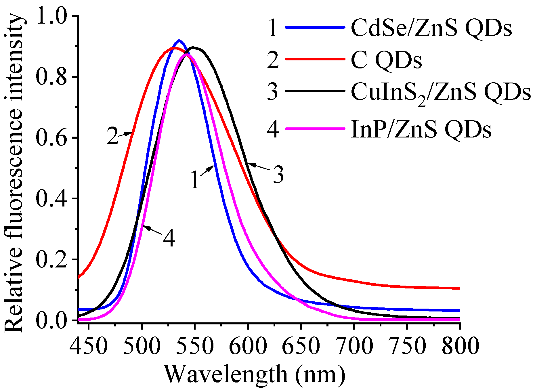
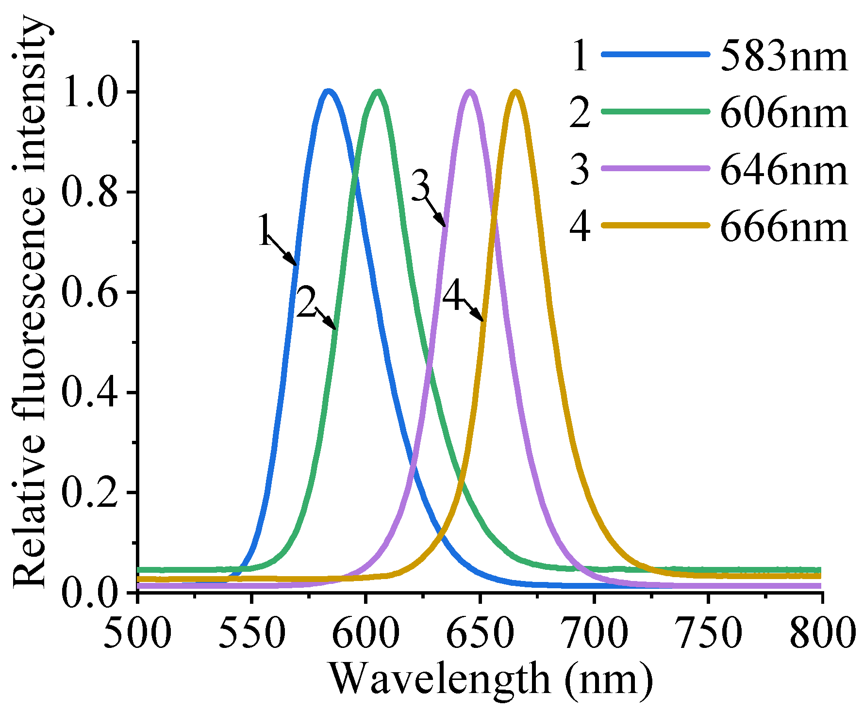
3.1. QD Characterization

Typical QDs composed of various elements—CdSe/ZnS QDs, C QDs, InP/ZnS QDs, and CuInS2/ZnS QDs —were selected as research objects and subjected to a range of experiments to determine whether analysis of the fluorescence lifetimes of QDs could reveal more morphological details of SSD in lapped optical components than analysis of the fluorescence intensities of QDs. In addition, it should be stated that the QDs used in this paper were purchased from Xingzi New Material Technology Development Co., Ltd. All of the QDs were spherical and aqueous. The F98 fluorescence spectrometer and the QuantaMaster8000 transient steady-state fluorescence spectrometer were used to characterize the fluorescence spectrum and fluorescence lifetime of the QDs, respectively.
To compare the SSD detection achieved by analyzing the QD fluorescence intensities with that achieved by analyzing the QD fluorescence lifetimes and explore the effect of the elemental composition of QDs on the QD fluorescence lifetime-based detection of the morphological details of SSD, CdSe/ZnS QDs, C QDs, InP/ZnS QDs, and CuInS2/ZnS QDs with similar sizes were selected for the study, and their fluorescence spectra are shown in Figure 2. As can be seen, their fluorescence peaks were all at 544 nm ± 10 m, so the fluorescence lifetime images of SSD were collected at this wavelength.
The fluorescence lifetime of core–shell QDs is not only related to the nature of the shell material but also strongly sensitive to the nanocrystal size due to quantum confinement effects, which also causes the fluorescence spectrum of the QDs to be blue-shifted as the core size decreases [27,28]. In general, the fluorescence lifetime of core–shell QDs increases with the increase in the core size and the decrease in the shell size. Therefore, to explore the effect of the size/fluorescence lifetime of QDs on the QD fluorescence lifetime-based detection, size-control methods were applied to generate four groups of core–shell CdSe/ZnS QDs with various fluorescence lifetimes. The fluorescence spectra of these four groups of CdSe/ZnS QDs are shown in Figure 3. The fluorescence peak, fluorescence lifetime, and diameter of these QDs are shown in Table 1. The QD diameters were all obtained by TEM.

3.2. QD Tagging of SSD in Optical Components

Williams et al., demonstrated that QDs can be added to lapping slurries to tag the SSD in optical components [12]. Therefore, QD-tagged diamond lapping slurry is used to process fused quartz optical components with a diameter and thickness of 25 mm and 3 mm, respectively. Before being used in this experiment, these components were fully polished to remove SSD arising from prior grinding or lapping. The detailed experimental parameters and steps are shown in Table 2. After processing, the optical components were cleaned ultrasonically with ethanol solution for 5 min to remove impurities and residual QDs on the surface fully. A 10 mg dose of each group of QDs was used in the experiments.

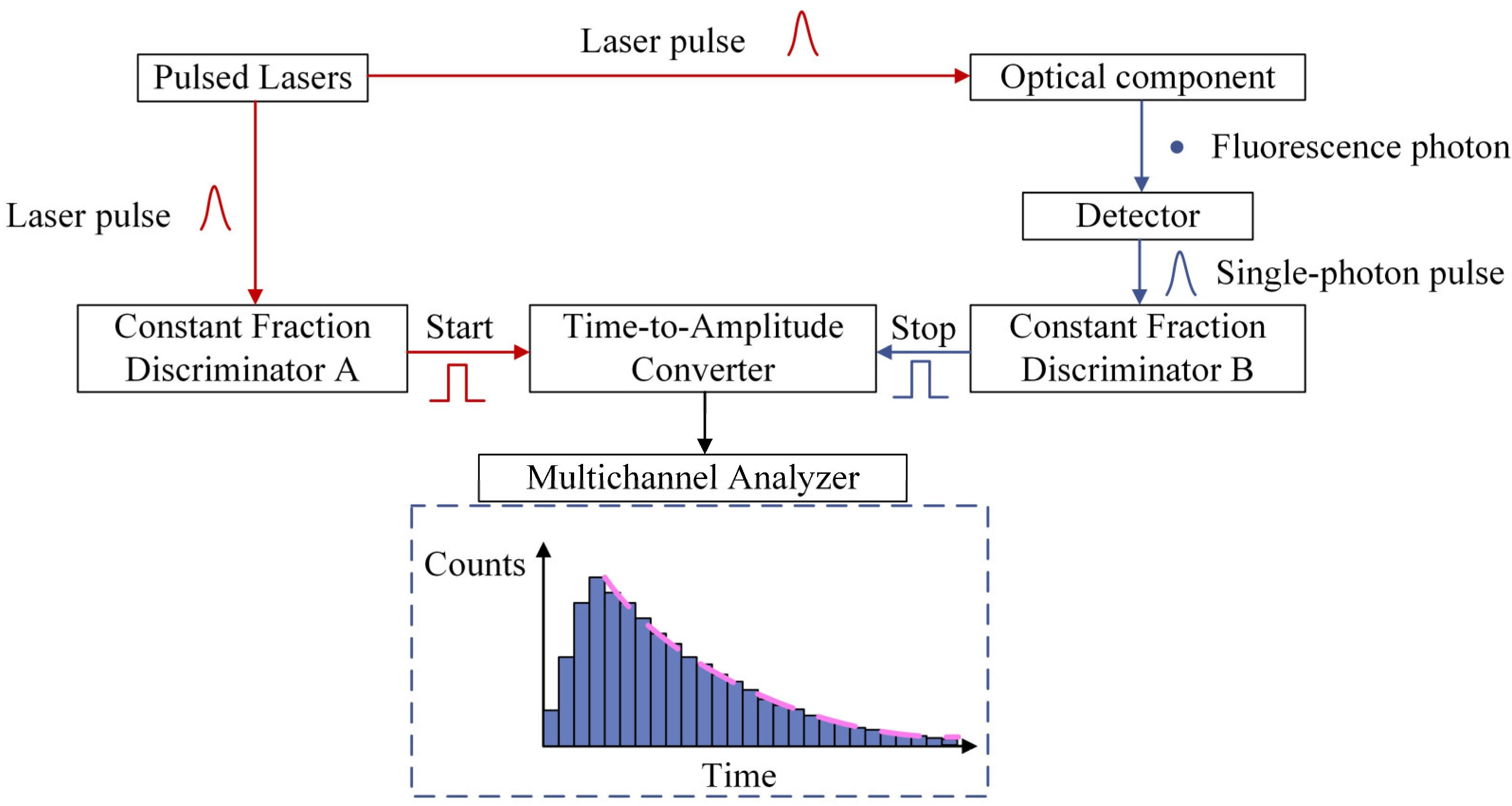
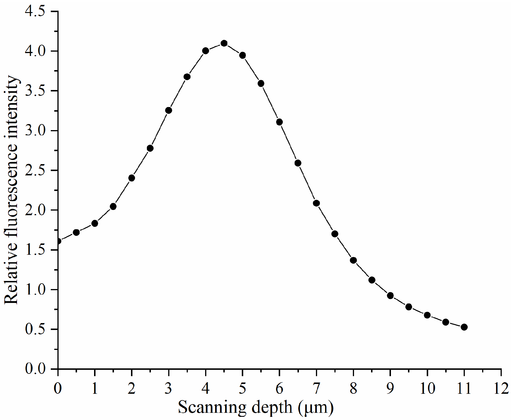
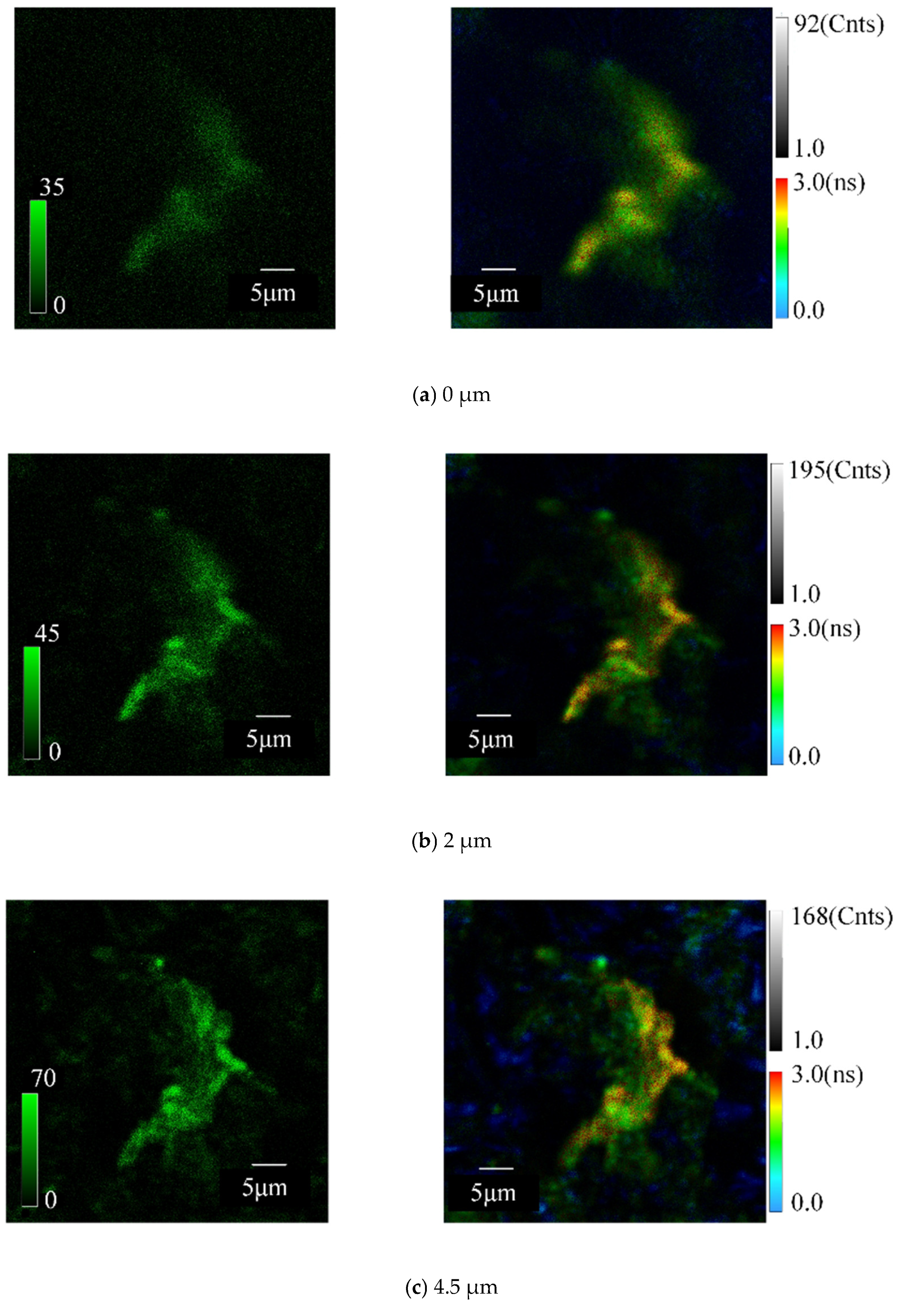
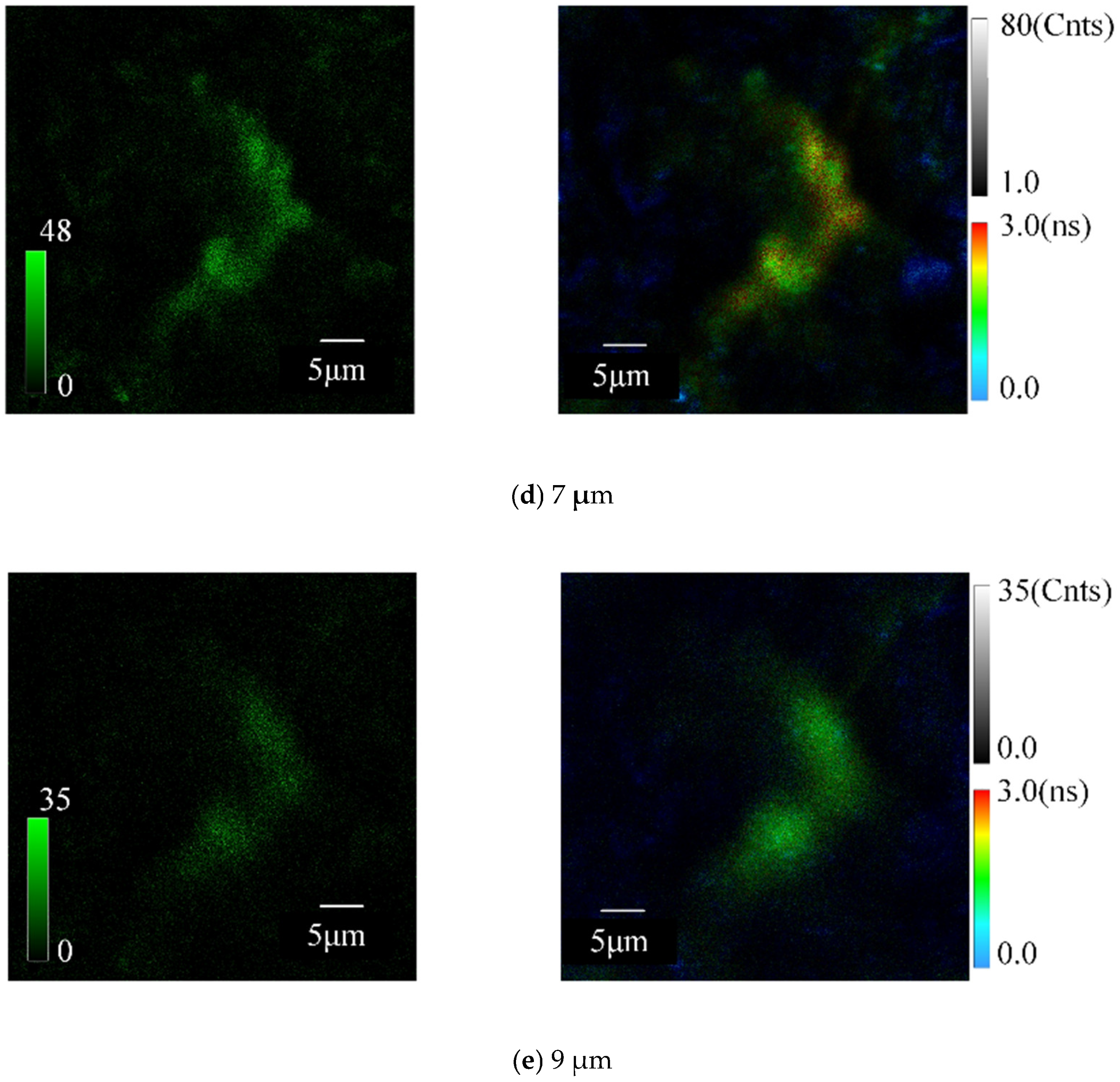
3.3. Acquisition and Characterization of Fluorescence Intensity and Fluorescence Lifetime Images of SSD in Lapped Optical Components

The fluorescence intensity images of SSD were collected on a Leica TCS SP8 STED 3X laser confocal microscope, and then a TCSPC system was built on this microscope to collect the fluorescence lifetime images of SSD. The SSD detection system used in this paper is shown in Figure 4 and enables the simultaneous acquisition of fluorescence intensity images and fluorescence lifetime images. In this system, the detector is a PicoHarp 300, and its spectral range is 470–670 nm. The light source is a white light laser, and the excitation wavelength, pulse frequency, and power are 470 nm, 80 MHz, and 1 mW, respectively. The pulse waveform is a square wave. All of the images were collected at room temperature, which is about 21 °C.
This system calibrates the refractive index using a 0.17 mm coverslip as the standard medium, thereby determining the point spread function. Moreover, the objective lens used in our experiment is an HC PL APO CS2 10×/0.40 DRY. The depth of focus of this objective lens is fixed, so it does not affect the movement of the focus. When testing, the specimen replaces the coverslip, so the refractive index and point spread function are constant during the layer-by-layer scanning process and do not affect the chromatographic data acquisition. This ensures that the SSD depth determined from the chromatographic data is correct and reliable.
The acquired fluorescence lifetime data of SSD were analyzed according to bi-exponential fitting using SymPho Time 64 (Version number: 2.1.3764) software to obtain the fluorescence lifetime image of the SSD, and the residuals were ± 30 ps. In this software, χ2 represents the fitting accuracy, and the fluorescence lifetimes are fitted using the χ2 close to 1. χ2 is defined as follows:
χ 2 = i = 1 N d i f i d i
where N is the number of test samples, di denotes the probability that the sample value falls into the i’th interval in N trials, and fi denotes the frequency that the sample value falls into the i’th interval in N trials.
Fourier transformation was applied to obtain the frequency spectrograms of the SSD images, and these spectrograms were then centralized, i.e., the center of each image spectrum was moved from the matrix origin (in the upper left corner) to the matrix center. This afforded frequency spectrograms in which the low-frequency signals and high-frequency signals (representing detailed features) were located in the center and on the perimeter, respectively. Then, the distributions of high-frequency signals were analyzed to determine the richness of the SSD morphological details. In addition, to improve the visibility of the detailed features of the SSD, the spectrogram was logarithmically transformed.
To simplify the characterization of the spectral features of the SSD, the spectra of the SSD were transformed into polar coordinates and represented by the function S(r,θ), where r and θ are variables in the polar coordinate system. For each determined direction θ, S(r,θ) is a one-dimensional function Sθ(r), which can be used to analyze the behavioral characteristics of the spectrum in a certain radial direction from the origin; for each determined frequency r, S(r,θ) is a one-dimensional function Sr(θ), which can be used to analyze the behavioral characteristics of the spectrum from a circle centered at the origin. The radial distribution feature S(r) and the angular distribution feature S(θ) of the spectral energy can be obtained by summing the subscripts of the functions Sθ(r) and Sr(θ), respectively, as follows:
S r = θ = 0 π S θ r
S θ = r = 1 R 0 S r θ
where R0 is the radius of the circle centered at the origin.
The mean of the angular distribution feature Sθ and the mean of the radial distribution feature Sr can be obtained by taking the mean of S(θ) and S(r), respectively.
In Section 4.1 and Section 4.2, the richness of the features detailed in the SSD is analyzed using 3D spectrograms; in Section 4.3, the richness of the features detailed in the SSD is analyzed by Sθ and Sr.

4. Results and Discussion

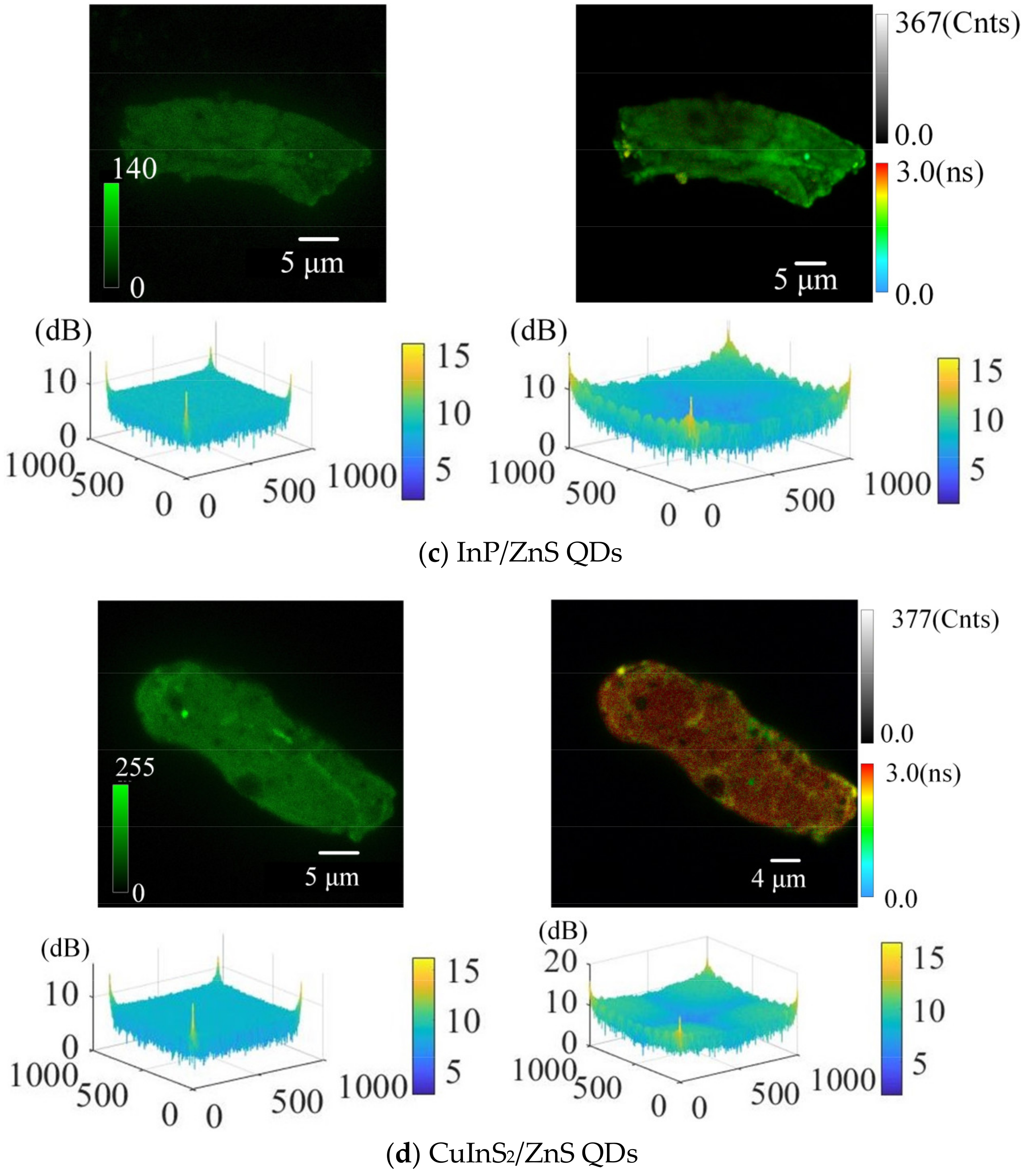
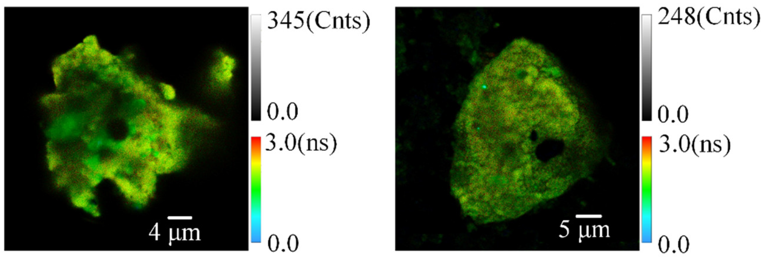
4.1. Comparison of SSD Detection Achieved by Analysis of QD Fluorescence Intensities with That Achieved by Analysis of QD Fluorescence Lifetimes

A damage point was selected on the lapped optical component tagged with CdSe/ZnS QDs, C QDs, InP/ZnS QDs, or CuInS2/ZnS QDs, and each point’s fluorescence intensity image, fluorescence lifetime image, and frequency spectrogram were obtained. The results are shown in Figure 5. In the fluorescence lifetime image, the color indicates the magnitude of the fluorescence lifetime, and the red and blue indicate upregulation and downregulation, respectively; the gray scale represents the number of photons, and larger gray values indicate higher numbers of photons. In the frequency spectrogram, colors indicate energy values of the image. The yellow and blue indicate upregulation and downregulation, respectively.
It should be stated that the optical components tested here are the optical components of groups 1–4 in Table 2.
Figure 5 indicates that QDs with different element compositions were able to detect the fluorescence intensity and fluorescence lifetime images of SSD, rather than only certain QDs being able to image the fluorescence intensity and fluorescence lifetime of SSD. Compared with the high-frequency signals in the fluorescence intensity images, those in the fluorescence lifetime images were stronger, which means that using the fluorescence lifetime of QDs as imaging contrast revealed more SSD details than using the fluorescence intensity of QDs as imaging contrast. This detection was unaffected by the elemental composition of the QDs. In addition, the SSDs were mostly “solid” dots and strips with obvious textural features.
In addition to the “solid” dot and strip SSDs shown in Figure 5, SSDs with “holes” were also detected, as shown in Figure 6, where the left image is from the C QD-tagged component and the right image is from the CdSe/ZnS QD-tagged component. Here, it should be explained that the “solid” SSD is the SSD in which the area formed by the edge of the SSD is a single connected area and there are no internal holes. SSD with “holes” means that there are obvious holes within the SSD and that there are holes in the area formed by the edge of the SSD, i.e., the area formed by the edge of the SSD is a multi-connected area.

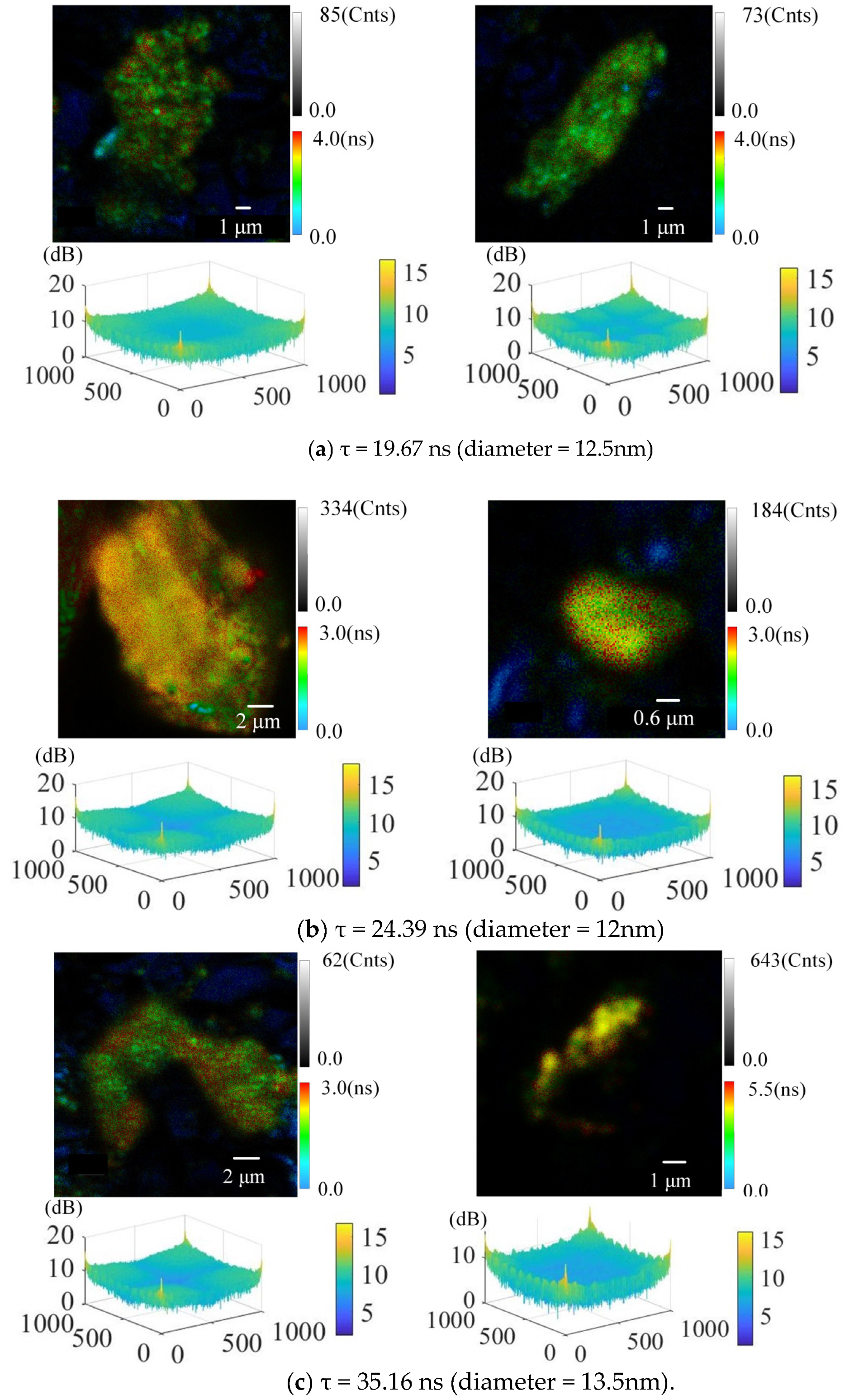
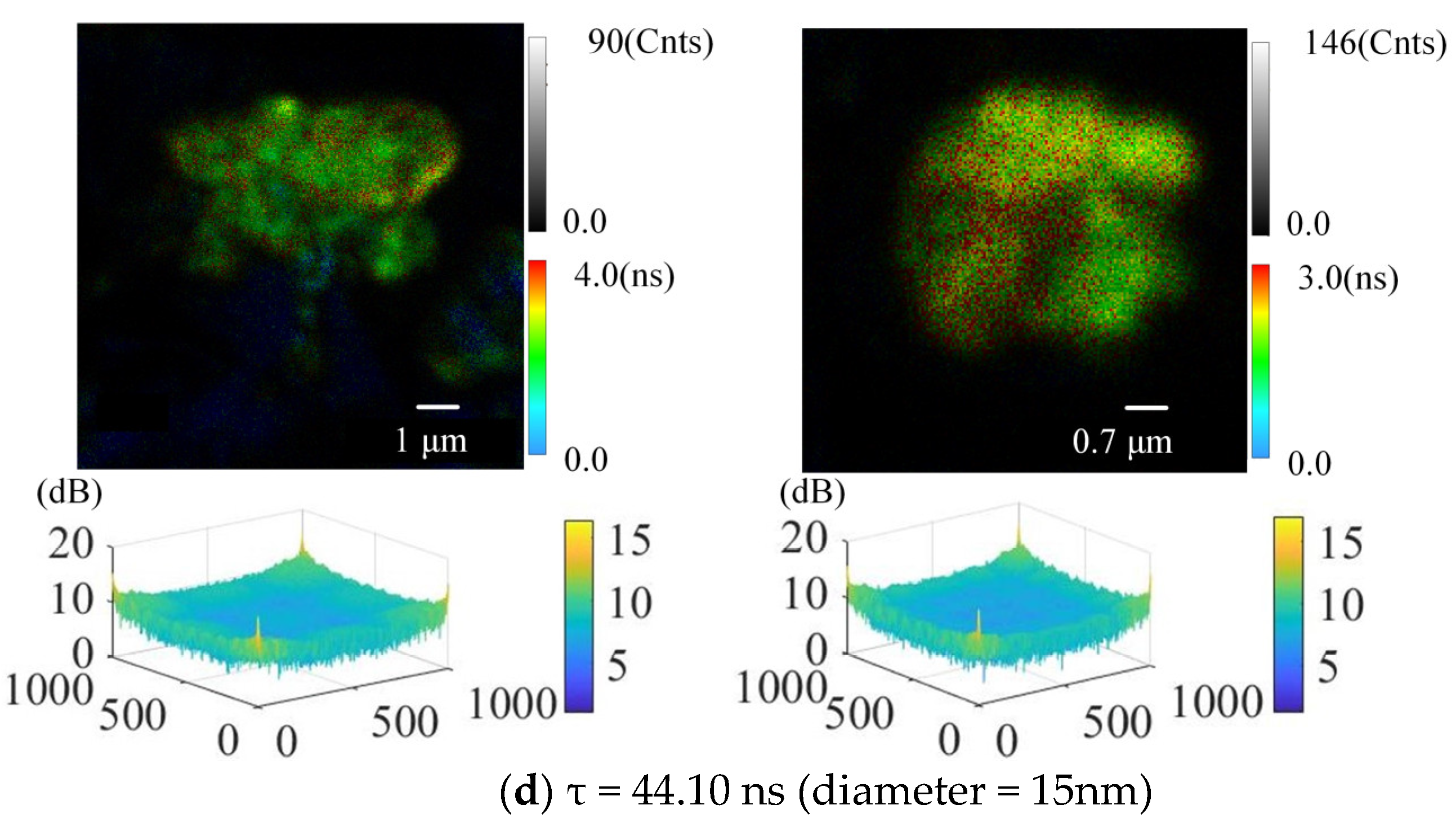
4.2. The Effect of the Size/Fluorescence Lifetime of QDs on the Detection of SSD Details

The fluorescence lifetime images of the SSD in lapped optical components tagged by CdSe/ZnS QDs with different sizes/fluorescence lifetimes were collected at the corresponding peak and their frequency spectrograms were extracted. Two SSD points on each group of optical components were subjected to this analysis, and the results are shown in Figure 7. It should be stated that the optical components tested here are the optical components of groups 5–8 in Table 2.
Figure 7 shows that the fluorescence lifetime values of QDs entering the SSD were reduced to different degrees (fluorescence lifetime of QDs reduced from tens of nanoseconds to a few nanoseconds), and the high-frequency signals of SSD were all strong, which means that the detection of SSD details was unaffected by the size/fluorescence lifetime of QDs. The decrease in the fluorescence lifetime of QDs can be explained by the excited-state lifetime theory. When the fluorescent molecules of QDs are irradiated by light, the electrons in the molecules absorb photons and jump from the ground state to the excited state. The electrons in the excited state are not stable in energy, and they lose their energy through radiative and non-radiative leaps to return to the excited state. Non-radiative leaps are energy consumed through non-photomorphic forms. Radiative leaps release energy in the form of photons, and fluorescence is a radiative leap phenomenon. Therefore, the fluorescence lifetime of QDs is mainly determined by the lifetime of spontaneous radiation, which is sensitive to the environment. When QDs are embedded in the SSD, the internal environment of the SSD causes the QDs to produce non-radiation to lose the excitation energy of electrons, which decreases the lifetime of the spontaneous radiation of the QDs. Therefore, the fluorescence lifetime of QDs in SSDs is decreased.
It should also be stated that, in addition to the images in Figure 5, Figure 6 and Figure 7, many fluorescence lifetime images of SSD at different times and on different components (containing different groups of components and different components in each group) were also collected, fully illustrating the repeatability of the experimental results presented in this paper.

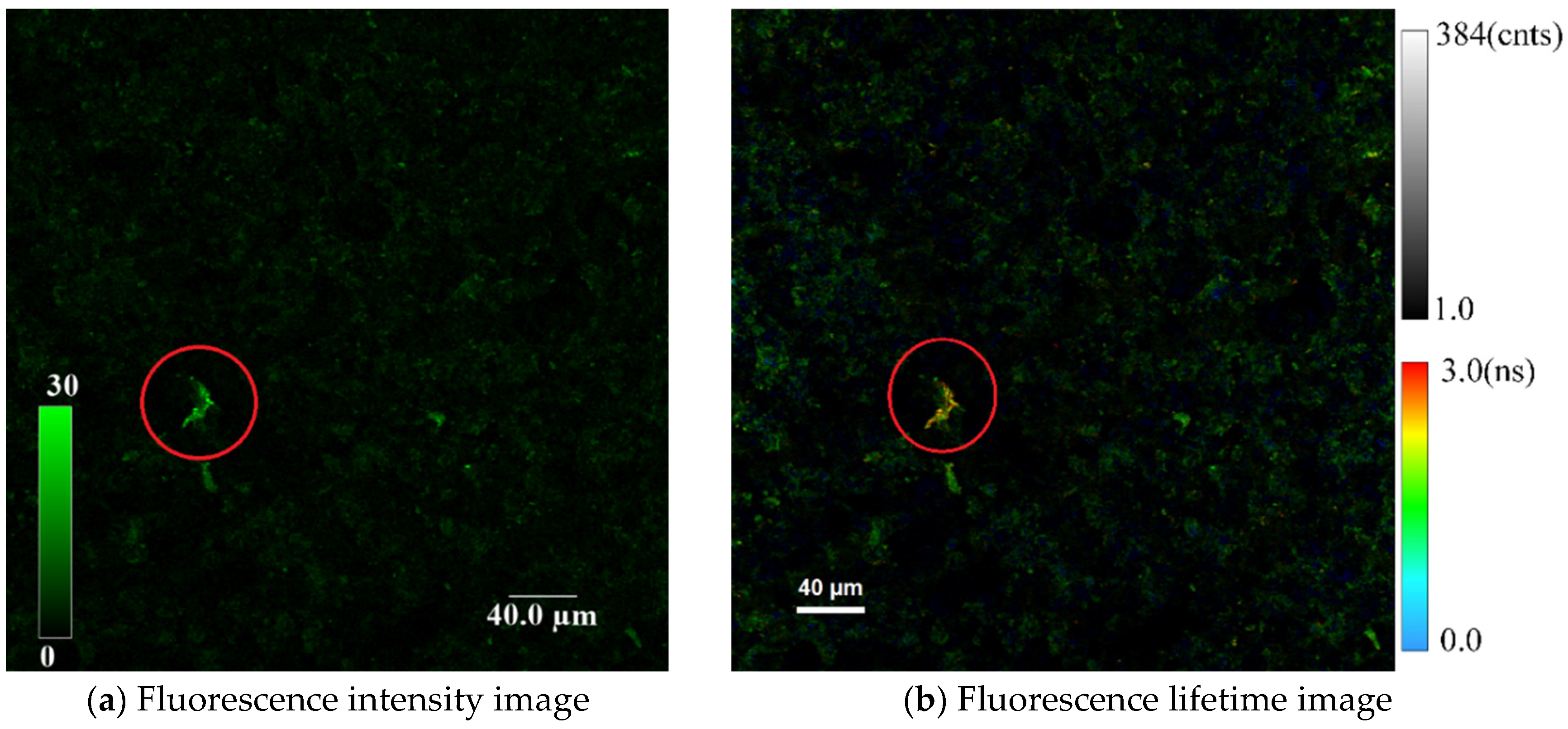
4.3. Comparison of Morphological Details at Different SSD Depths

For the optical components of group 5 in Table 2, an arbitrary region was selected for fluorescence intensity imaging and fluorescence lifetime imaging, and the SSD distribution in this region is shown in Figure 8, which indicates that the detection of SSD distribution can be achieved by analysis of the QD fluorescence lifetimes, similar to that achieved by analysis of QD fluorescence intensities.
Fluorescence intensity-based chromatography scans and fluorescence lifetime -based chromatography scans were performed for the SSD marked by the red circle in this region. The chromatographic scan interval was 0.5 µm. The variation in the fluorescence intensity of the SSD with the scanning depth is shown in Figure 9, which indicates that the depth of this SSD was 4.5 µm. Figure 10 shows the fluorescence intensity images and fluorescence lifetime images of this damage point at partial chromatographic depth. For the fluorescence intensity images and fluorescence lifetime images at different scanning depths, the mean of the angular distribution feature Sθ and the mean of the radial distribution feature Sr were calculated. Figure 11 shows the variation in the Sr, Sθ with the scanning depth.
Figure 11 shows that the variation in Sr-τ, Sr-i, Sθ-τ, and Sθ-i with scanning depth was consistent and that Sr-τ and Sθ-τ peaked at the depth of SSD (i.e., 4.5 µm), indicating that the depth of SSD can be determined according to the variation in the Sr-τ or Sθ-τ with the scanning depth. In addition, the Sr-τ > Sr-i and Sθ-τ > Sθ-i always held for any scanning depth, indicating that the SSD detection achieved by analyzing the QD fluorescence lifetime can detect more SSD details on the premise of achieving the detection of SSD depth.
Based on the above analysis, the SSD detection of the fluorescence intensity-based method and fluorescence lifetime-based method were compared, as shown in Table 3.

5. Conclusions

This study develops a new method for non-destructively and accurately detecting the morphology of SSD in lapped optical components by analysis of the fluorescence lifetimes of QDs. The SSD detection achievable based on the analysis of QD fluorescence intensity is compared with that achievable based on the analysis of QD fluorescence lifetime. The following two key findings were made: (1) Compared with the method that uses the fluorescence intensity of QDs to detect SSD, the new method reveals more morphological details of SSD in lapped optical components on the premise of achieving the detection of SSD distribution and depth, and the detection of SSD details is unaffected by the elemental composition/size/fluorescence lifetime of QDs. (2) the SSD of the optical components exhibits textural features, with “hole”-type SSD detected in addition to “solid” point and strip SSD. These findings will facilitate the exploration of the formation mechanism of SSD in optical components, thereby enabling the improvement of optical manufacturing techniques.
In addition, it is worth stating that the fluorescence intensity-based method takes about 5 s to acquire the image, and the fluorescence lifetime-based method takes about 51 s to acquire the image, which suggests that the image acquisition speed of the fluorescence lifetime-based method needs to be further improved in the future.

Author Contributions

Investigation, Y.C., Z.L., R.L. and W.H.; methodology, Y.C.; supervision, C.W., X.L. and Y.W.; writing—original draft, Y.C.; writing—review and editing, Y.C. All authors have read and agreed to the published version of the manuscript.

Funding

This research was funded by Xi’an Key Laboratory of Active Photoelectric Imaging Detection Technology.

Data Availability Statement

The data used to support the findings of this study are included within the article.

Acknowledgments

The authors sincerely appreciate the Xi’an Key Laboratory of Active Photoelectric Imaging Detection Technology for the funding support and the Instrumental Analysis Center of Xi’an Jiaotong University for providing the Leica TCS SP8 STED 3X laser confocal microscope.

Conflicts of Interest

The authors declare no conflict of interest.

References

  1. Neauport, J.; Ambard, C.; Cormont, P.; Darbois, N.; Rondeau, O. Subsurface damage measurement of ground fused silica parts by HF etching techniques. Opt. Express 2009, 17, 20448–20456. [Google Scholar] [CrossRef] [PubMed]
  2. Zhang, B.; Howes, T.D. Material-Removal Mechanisms in Grinding Ceramics. CIRP Ann.—Manuf. Technol. 1994, 43, 305–308. [Google Scholar] [CrossRef]
  3. Wu, S.L.W.Z.Y. Relationship between subsurface damage and surface roughness of optical materials in grinding and lapping processes. J. Mater. Process. Technol. 2008, 205, 34–41. [Google Scholar] [CrossRef]
  4. Temple, P.A. Total Internal Reflection Microscopy: A Surface Inspection Technique. Appl. Opt. 1981, 20, 2656–2664. [Google Scholar] [CrossRef]
  5. Bertussi, B.; Cormont, P.; Palmier, S.; Legros, P.; Rullier, J.L. Initiation of laser-induced damage sites in fused silica optical components. Opt. Express 2009, 17, 11469–11479. [Google Scholar] [CrossRef] [PubMed]
  6. Duncan, M.D.; Bashkansky, M.; Reintjes, J. Subsurface defect detection in materials using optical coherence tomography. Opt. Express 1998, 2, 540–545. [Google Scholar] [CrossRef] [PubMed]
  7. Bismayer, U.; Brinksmeier, E.; Güttler, B.; Seibt, H.; Menz, C. Measurement of subsurface damage in silicon wafers. Precis. Eng. 1994, 16, 139–144. [Google Scholar] [CrossRef]
  8. Lee, Y. Evaluating subsurface damage in optical glasses. J. Eur. Opt. Soc. Rapid Publ. 2011, 6, 11001. [Google Scholar]
  9. Rossetti, R.; Nakahara, S.; Brus, L.E. Quantum size effects in the redox potentials, resonance Raman spectra, and electronic spectra of CdS crystallites in aqueous solution. J. Chem. Phys. 1983, 79, 1086–1088. [Google Scholar] [CrossRef]
  10. Klar, T.A.; Jakobs, S.; Dyba, M.; Egner, A.; Hell, S.W. Fluorescence microscopy with diffraction resolution barrier broken by stimulated emission. Proc. Natl. Acad. Sci. USA 2000, 97, 8206–8210. [Google Scholar] [CrossRef]
  11. Stephan, T.; Roesch, A.; Riedel, D.; Jakobs, S. Live-cell STED nanoscopy of mitochondrial cristae. Sci. Rep. 2019, 9, 12419. [Google Scholar] [CrossRef] [PubMed]
  12. Williams, W.B.; Mullany, B.A.; Parker, W.C.; Moyer, P.J.; Randles, M.H. Using quantum dots to tag subsurface damage in lapped and polished glass samples. Appl. Opt. 2009, 48, 5155–5163. [Google Scholar] [CrossRef]
  13. Williams, W.; Mullany, B.; Parker, W.; Moyer, P.; Randles, M. Using quantum dots to evaluate subsurface damage depths and formation mechanisms in glass. CIRP Ann.—Manuf. Technol. 2010, 59, 569–572. [Google Scholar] [CrossRef]
  14. Williams, W.B.; Mullany, B.A.; Moyer, P.J.; Parker, W.C.; Randles, M.H. Characterizing quantum dots for use in detecting subsurface damage. In Proceedings of the 23rd Annual Meeting of the American Society for Precision Engineering, Portland, OR, USA, 19–24 October 2008; pp. 440–443. [Google Scholar]
  15. Williams, W.B.; Mullany, B.A.; Moyer, P.J.; Parker, W.C.; Randles, M.H. Testing quantum dots as a means of assessing subsurface damage in polished glass. In Proceedings of the 24th Annual Meeting of the American Society For Precision Engineering, Monterey, CA, USA, 4–9 October 2009. [Google Scholar]
  16. Williams, W.; Mullany, B.; Parker, W.; Moyer, P. Evaluating Subsurface Damage with Quantum Dots. In Proceedings of the Optical Fabrication and Testing 2010, Jackson Hole, WY, USA, 13–17 June 2010. [Google Scholar]
  17. Williams, W.B. A Novel Fluorescence Based Method of Assessing Subsurface Damage in Optical Materials; The University of North Carolina: Charlotte, NC, USA, 2009. [Google Scholar]
  18. Hong-Xiang, W.; Jing, H.; Jing-He, W.; Ben-Wen, Z.; Yan-Hu, Z. Experimental investigation of subsurface damage depth of lapped optics by fluorescent method. J. Cent. South Univ. 2018, 25, 1678–1689. [Google Scholar] [CrossRef]
  19. Cui, Y.; Wang, C.; Liu, X.; Gao, R.; Li, T. Subsurface damage detection of optical elements by analyzing the photobleaching properties of quantum dots. Precis. Eng. 2022, 77, 24–32. [Google Scholar] [CrossRef]
  20. Cheng, X.; Hinde, E.; Owen, D.M.; Lowe, S.B.; Reece, P.J.; Gaus, K.; Gooding, J.J. Enhancing Quantum Dots for Bioimaging using Advanced Surface Chemistry and Advanced Optical Microscopy: Application to Silicon Quantum Dots (SiQDs). Adv. Mater. 2015, 27, 6144–6150. [Google Scholar] [CrossRef] [PubMed]
  21. Goreham, R.V.; Schroeder, K.L.; Holmes, A.; Bradley, S.J.; Nann, T. Demonstration of the lack of cytotoxicity of unmodified and folic acid modified graphene oxide quantum dots, and their application to fluorescence lifetime imaging of HaCaT cells. Microchim. Acta 2018, 185, 128. [Google Scholar] [CrossRef]
  22. Shang, L.; Yang, L.; Wang, H.; Nienhaus, G.U. In Situ monitoring of the intracellular stability of nanoparticles by using fluorescence lifetime imaging. Small 2016, 12, 868–873. [Google Scholar] [CrossRef]
  23. Steponkiene, S.; Valanciunaite, J.; Skripka, A.; Rotomskis, R. Cellular Uptake and Photosensitizing Properties of Quantum Dot-Chlorin e(6) Complex: In Vitro Study. J. Biomed. Nanotechnol. 2014, 10, 679–686. [Google Scholar] [CrossRef]
  24. Cui, Y.; Wang, C.; Liu, X.; Gao, R.; Li, T. Technology for subsurface damages detection of optical components based on various fluorescent material. In Proceedings of the AOPC 2022: Novel Optical Design; and Optics Ultra Precision Manufacturing and Testing, Beijing, China, 20 January 2023; pp. 5–13. [Google Scholar]
  25. Bian, F.; Sun, L.; Cai, L.; Wang, Y.; Zhao, Y. Quantum dots from microfluidics for nanomedical application. Wiley Interdiscip. Rev. -Nanomed. Nanobiotechnol. 2019, 11, e1567. [Google Scholar] [CrossRef]
  26. Suhling, K.; Hirvonen, L.M.; Levitt, J.A.; Chung, P.-H.; Tregidgo, C.; Le Marois, A.; Rusakov, D.A.; Zheng, K.; Ameer-Beg, S.; Poland, S.J.M.P. Fluorescence lifetime imaging (FLIM): Basic concepts and some recent developments. Med. Photonics 2015, 27, 3–40. [Google Scholar] [CrossRef]
  27. Hemdana, I.; Mahdouani, M.; Bourguiga, R. Investigation of the radiative lifetime in core-shell CdSe/ZnS and CdSe/ZnSe quantum dots. Phys. B-Condens. Matter 2012, 407, 3313–3319. [Google Scholar] [CrossRef]
  28. Kaur, G.; Tripathi, S.K. Probing photoluminescence dynamics of colloidal CdSe/ZnS core/shell nanoparticles. J. Lumin. 2014, 155, 330–337. [Google Scholar] [CrossRef]
Figure 1. The principle of TSCPC–FLIM.
Electronics 12 03868 g001
Figure 2. Fluorescence spectra of QDs composed of different elements.
Electronics 12 03868 g002
Figure 3. Fluorescence spectra of CdSe/ZnS QDs with different fluorescence lifetimes.
Electronics 12 03868 g003
Figure 4. The SSD detection system used in this paper.
Electronics 12 03868 g004
Figure 5. Fluorescence intensity/fluorescence lifetime images of SSDs in lapped optical components and their spectrograms (in (ad), upper left corner: fluorescence intensity image; upper right corner: fluorescence lifetime image; lower left corner: frequency spectrogram of fluorescence intensity image; lower right corner: frequency spectrogram of fluorescence lifetime image). The optical components here are tagged with the QDs composed of various elements—CdSe/ZnS QDs, C QDs, InP/ZnS QDs, and CuInS2/ZnS QDs. The units of the X and Y axes of the spectrogram are 1/nm.
Electronics 12 03868 g005aElectronics 12 03868 g005b
Figure 6. SSDs with “holes” ((Left) image is from the C QD-tagged component and the (right) image is from the CdSe/ZnS QD-tagged component.).
Electronics 12 03868 g006
Figure 7. Fluorescence lifetime images of SSDs in lapped optical components tagged by CdSe/ZnS QDs with different sizes/fluorescence lifetimes and their spectrograms (in (ad), upper left corner and upper right corner: fluorescence lifetime images; lower left corner and lower right corner: frequency spectrogram of fluorescence lifetime images). The units of the X and Y axes of the spectrogram are 1/nm.
Electronics 12 03868 g007aElectronics 12 03868 g007b
Figure 8. Fluorescence intensity imaging and fluorescence lifetime imaging of the SSD distribution. The optical components here are tagged with CdSe/ZnS QDs (τ = 24.39 ns), and a fluorescence intensity-based chromatography scan and a fluorescence lifetime-based chromatography scan are performed for the SSD marked by the red circle.
Electronics 12 03868 g008
Figure 9. The variation in the fluorescence intensity of the SSD (marked by the red circle) with the scanning depth.
Electronics 12 03868 g009
Figure 10. The fluorescence intensity image and fluorescence lifetime image of the SSD (marked by the red circle) at partial chromatographic depth (in (ae), left: fluorescence intensity images; right: fluorescence lifetime images).
Electronics 12 03868 g010aElectronics 12 03868 g010b
Figure 11. The variation in Sr, Sθ with scanning depth. (Sr-τ: the Sr of the fluorescence lifetime image; Sr-i: the Sr of the fluorescence intensity image; Sθ-τ: the Sθ of the fluorescence lifetime image; Sθ-i: the Sθ of the fluorescence intensity image.).
Electronics 12 03868 g011
Table 1. Fluorescence peaks, fluorescence lifetimes, and diameters of the QDs shown in Figure 3.
Fluorescence PeaksFluorescence Lifetime τ (ns)Diameter (nm)
58324.3912
60619.6712.5
64635.1613.5
66644.1015
Table 2. Processing parameters and steps of optical components.
Serial NumberElemental Composition of QDsFluorescence Peaks (nm)Processing Parameters and Steps
1CdSe/ZnS QDs544(1) D30 diamond lapping slurry, 5 min, lapping speed = 54 rad/min;
(2) D6 diamond lapping slurry, 3 min, lapping speed = 54 rad/min.
2C QDs544
3InP/ZnS QDs544
4CuInS2/ZnS QDs544
5CdSe/ZnS QDs583
6CdSe/ZnS QDs606
7CdSe/ZnS QDs646
8CdSe/ZnS QDs666
Table 3. The comparison of the SSD detection of the fluorescence intensity-based method and the fluorescence lifetime-based method.
Characterization of SSDFluorescence Intensity-Based MethodFluorescence Lifetime-Based Method
DistributionCan be detected
DepthCan be detected
MorphologyLow detection accuracyHigh detection accuracy
Disclaimer/Publisher’s Note: The statements, opinions and data contained in all publications are solely those of the individual author(s) and contributor(s) and not of MDPI and/or the editor(s). MDPI and/or the editor(s) disclaim responsibility for any injury to people or property resulting from any ideas, methods, instructions or products referred to in the content.

