Review

Topologies and Design Characteristics of Isolated High Step-Up DC–DC Converters for Photovoltaic Systems

School of Electronics, Electrical Engineering and Computer Science (EEECS), Queen’s University, Belfast BT9 5AH, UK
*
Author to whom correspondence should be addressed.
Electronics 2023, 12(18), 3913; https://doi.org/10.3390/electronics12183913
Submission received: 27 June 2023 / Revised: 23 August 2023 / Accepted: 29 August 2023 / Published: 16 September 2023
(This article belongs to the Section Power Electronics)

Abstract

:
This paper aims to investigate the state-of-the-art isolated high-step-up DC–DC topologies developed for photovoltaic (PV) systems. This study categorises the topologies into transformer-based and coupled inductor-based converters, as well as compares them in terms of various parameters such as component count, cost, voltage conversion ratio, efficiency, voltage stress, input current ripple, switching mode, and power rating. The majority of the topologies examined exhibit peak efficiencies of 90% to 97%, with voltage conversions in excess of eight, as well as power ratings ranging from 100 W to 2 kW. The existing literature has found that most isolated DC–DC converters increase their turn ratios in order to achieve high step-up ratios. As a result, voltage spikes have increased significantly in switches, resulting in a decrease in overall system efficiency. In this research, the use of passive and active snubbers to provide soft switching in isolated step-up DC–DC converters is investigated. Moreover, a comprehensive analysis of the three most widely used boost techniques is provided. A reduction in turn ratio and a decrease in voltage stress were the results of this process. The main purpose of this study is to provide a comprehensive overview of the most used high-boost isolated DC–DC topologies in PV systems, including flyback, isolated SEPIC, forward, push-pull, half- and full-bridge, and resonant converter, with a focus on the recent research in the field and the recent advancements in these topologies. This study aims to guide further research and analysis in selecting appropriately isolated topologies for PV systems.

1. Introduction

The demand for electrical energy has risen significantly due to population growth and the expansion of various industries. Currently, most of the energy consumed is obtained from fossil fuels, which contribute to global warming through the emission of harmful gases. To address these concerns, renewable energy sources (RESs) such as solar, wind, geothermal, hydropower, and biomass have gained increased attention so as to combat climate change and ensure energy security. According to the estimates made in [1], if fossil fuels were replaced with RESs by the year 2050, the world would be able to save a total of $12 trillion. However, the variable and unpredictable nature of RESs present challenges regarding their output voltage. To provide the necessary voltage to the load, an intermediate circuit, such as a DC–DC converter, is often needed to boost the voltage of the RES. The integration of RESs into the power grid has led to a growing demand for electronic power converters. Recent technological advancements in various fields, such as PV, wind power, electric vehicles, energy storage, and power supply, have increased the demand for high-step DC–DC converters. It is important for RESs to have reliable and efficient converters to ensure a stable and efficient power supply. Ongoing research is focused on improving factors such as efficiency, reliability, power density, and cost [2].
DC–DC converters are typically categorised into two different classifications: isolated and non-isolated. Topologies that are not isolated, such as buck, boost, cuk, zeta, and single-ended primary-inductor (SEPIC) converters, transfer power without magnetic isolation [3], and are utilised so as to obtain a substantial increase in voltage gain. In recent years, various non-isolated topologies for high step-up voltage gain have been developed. Techniques such as Interleave Boost (IB), Coupled Inductor (CI), Switched Capacitor (SC), Cascaded Boost (CB), Switched Inductor (SI), and Voltage Multiplier (VM) [4,5,6,7,8,9] have been employed to achieve a high voltage gain by appropriately adjusting the duty ratio. Nevertheless, these methods may suffer from inefficiencies caused by the need for an extensive amount of circuit components, and they may not meet the requirements for galvanic isolation [10].
Galvanic isolation is a critical requirement for safety reasons when connecting the grid to RESs as it ensures that the potential differences between the output and input sides of the topology do not pose a threat to human life or equipment [3]. For high step-up applications, particularly in the field of RESs, a new generation of isolated converters has been proposed to meet these safety requirements. Isolated converters offer higher step-up voltage gain and are suitable for applications where variable input voltages and load regulation are required [3]. Multiple-input and multiple-output (MIMO) topologies can be employed to achieve isolation between the input and output sides of a circuit. This isolation is particularly beneficial for sensitive loads that are prone to noise and defects. By including two separate ground references, the circuit can effectively mitigate any disturbances and ensure reliable operation [3]. By using either coupled inductors or transformers, these isolated topologies can convert DC to AC voltage, and they can then rectify the AC voltage back to the DC voltage. Compared to non-isolated topologies, they have a higher voltage conversion ratio [3] and higher efficiency [11]. Figure 1 illustrates an overview of DC–DC converter classifications for both categories of isolated and non-isolated converters.
Numerous research papers have been published in the literature about the modification of isolated DC–DC typologies for PV applications. Nevertheless, an extensive number of published reviews has been dedicated to non-isolated converters [4,9,12,13,14,15,16,17,18]. In contrast, there are few studies in the literature that examine isolated step-up converters in the context of PV applications [3,19,20,21]. This study aims to address the knowledge gaps in the existing literature by providing a comprehensive analysis of a variety of isolated high-step-up DC–DC converters. This work has shown many examples of high step-up isolated DC–DC converters, which have acquired significant recognition and use within the PV industry. The evaluation of the current configurations and control methodologies utilised by these converters is crucial in order to understand the operational mechanisms of isolated step-up converters in PV systems. Therefore, it is necessary to investigate new converter architectures and improve existing methodologies to enhance their operational efficiency, while also reducing their weight and size. Researchers are seeking to gain a comprehensive understanding of isolated high step-up DC–DC converters, and to accurately assess intricate topologies in order to evaluate their potential for achieving high voltage gains. The following are the objectives of the review:
1.
Examine a number of isolated DC–DC converters that have not previously been reviewed.
2.
Overview of the isolated DC–DC typologies for PV applications that enhance voltage conversion ratios and mitigate voltage stress by the utilisation of step-up techniques and snubbers.
3.
A study comparing isolated DC–DC converters for the component count, cost, voltage conversion ratio, voltage stress, input current ripple, switching mode, efficiency, and power rating.
4.
An outline of the benefits and drawbacks associated with different types of isolated DC–DC converter typologies and control mechanisms that have been presented with the aim of supporting future investigations in this field.
Table 1 presents an overview of the advantages and disadvantages associated with the main isolated DC–DC converter types that have been evaluated in the context of this study. The paper is structured into six sections. Following this introduction, Section 2 presents a brief overview of PV systems. Section 3 provides a categorisation of the main isolated DC–DC converters based on the type of isolation structure. Section 4 contains a detailed discussion about the soft- and hard-switched converters on isolated DC–DC converters. Section 5 discusses three popular techniques through which to achieve high power gains for isolated DC–DC converters. Section 7 discusses converter control. Section 8 highlights the opportunities and challenges of isolated DC–DC converters. Finally, Section 9 draws the conclusions.

2. Overview of PV System

PV systems have a lifespan of up to 20 years and offer lower maintenance costs due to their ability to withstand prolonged exposure to extreme weather conditions [22]. During 2020–2024, PV generation is expected to grow at an annual rate of 18% [21]. Within 20 years, it will be the largest source of renewable energy [9]. Arrays and inverters are the major components of a PV system. However, the system must also be equipped with additional components in order to function correctly. In PV production, a common problem is that the panels’ output voltage is much less than that of the grid. A single solar panel’s DC voltage is typically between (20 V–80 V) [23,24]. It is typically recommended to increase the output voltage to 200 V–600 V when connecting this source to an AC load or network [25].
Connecting PV cells in series can provide high voltage, but this is not practical due to the shadowing effect, where shading on one panel affects the performance of the entire string. Parallel cells are a solution to this problem, as shading on one panel in this arrangement does not affect the performance of the other panels. However, mismatches in voltage ratings can result in some panels operating at less-than-optimal levels. Therefore, the use of a high step-up DC–DC converter becomes necessary in order to boost the voltage for grid-tied PV systems. Figure 2 illustrates the general arrangement of a high step-up DC–DC converter employed in a PV system.
A high step-up DC–DC converter needs to be able to handle the peculiarities of the input current from PV panels, which require maximum power point tracking (MPPT). The goal of MPPT is to ensure that the solar panel is operating at its maximum power point, which is the point at which the panel produces the most power. This is important because the voltage and current output of a solar panel can vary due to changes in temperature, light intensity, and other factors. To implement MPPT, a specialised algorithm samples the PV panel’s output voltage and current before modifying the duty ratio accordingly. The Steady-State Time (SST) is important in MPPT as it informs the selection of an appropriate sampling time for the control algorithm. SST refers to the time it takes for the PV system to settle and stabilise at a new operating point after an MPPT algorithm has been adjusted. This settling time is crucial because it affects the accuracy and effectiveness of the MPPT algorithm. When choosing the sampling time for the MPPT algorithm, it is essential to consider the SST of the DC–DC converter. Suppose the sampling time is significantly shorter than the SST. In that case, the MPPT algorithm might introduce unnecessary fluctuations in the converter’s operation, leading to reduced efficiency and potentially even instability. On the other hand, if the sampling time is too long compared to the SST, the MPPT algorithm might not respond quickly enough to changes in operating conditions. In practice, sampling time is a trade-off between tracking speed and stability. It is crucial to analyse the characteristics of the specific PV system, the DC–DC converter, and the MPPT algorithm to determine an appropriate sampling time that balances these factors. A further development in control algorithms and hardware design has resulted in the development of more sophisticated MPPT techniques that can adapt to changes more effectively, as well as can reduce the impact of steady-state settling time on overall performance. Many papers have been studied and published on MPPT techniques [26,27,28,29,30,31,32]. MPPT requires a continuous input current in order to function correctly. A discontinuous input current can cause the MPPT of a PV system to deteriorate, and it can also negatively impact the system’s dynamic performance.
The National Electrical Code recommends that PV panels be isolated from the AC grid for safety; additionally, it also reduces the risk of potential-induced degradation (PID) to the PV panels, which is caused by the difference in voltage between the PV panel and the grid [33]. This is because when PV panels are connected to the AC grid, they can cause an imbalance in the electrical current. This can result in damage to the PV panel or the grid itself. As a result, there has been an increasing emphasis on the use of step-up isolated DC–DC converters for PV applications, primarily due to the safety advantages associated with isolation [34].

3. Isolated DC–DC Converters

It is essential to ensure galvanic isolation in DC–DC converters in order to guarantee reliable power transmission and to prevent Electromagnetic Interference (EMI) [35]. Isolated converters have been widely utilised at various power levels, often as modifications of non-isolated converters. DC–DC converters that are galvanically isolated can be classified as transformers or coupled inductors based on the energy transmission element. A popular arrangement is to locate coupled inductors or transformers near the source, where high-frequency voltage/current pulses are generated. Even though both transformers and coupled inductors are constructed using multiple windings on a magnetic core, their operating principles and roles in switching converters are quite different [36]. Transformer-based converters have been the preferred choice for providing galvanic isolation owing to their notable power density, and they are commonly used for applications requiring high power levels. On the other hand, coupled inductor-based converters offer a more efficient approach with a compact size and weight; in addition, they are commonly used in lower-power applications.

3.1. Coupled Inductor-Based Converters

Coupled inductor-based isolated DC–DC converters are primarily used for energy storage while the switch is active. The power that enters and exits the inductors is different, and this feature is exploited in converters such as flyback and isolated SEPIC converters. These converters are particularly useful in high step-up applications and are known for their coupled-inductor design [37]. One major advantage of flyback and isolated SEPIC converters is that they only require one switch, which makes them more straightforward, more reliable, and cost-effective compared to other isolated DC–DC converters. These features make them particularly desirable for cost-sensitive and reliability-critical applications, such as medical and automotive applications.

3.1.1. Flyback Converter Topologies

The flyback converter is widely employed in low-power applications including, but not limited to, personal computers, LCD televisions, cell phones, and notebooks as power supply circuits [38,39]. Further, it is well-suited for low-power PV applications [21]. However, the presence of a coupled inductor inside the circuit results in high leakage inductance, hence causing large voltage spikes upon the turn-off of the switch. This effect has a detrimental impact on the overall operational effectiveness and efficiency of the topology. Furthermore, the flyback converter demands a high peak current to charge the energy storage capacitor at the beginning of each switching cycle. This high peak current leads to a need for higher-rated components, which increases the converter’s cost. Figure 3a shows the conventional flyback converter comprises a power switch MOSFET or IGBT ( ( Q 1 ) ), a transformer ( ( T 1 ) ), a diode ( ( D o ) ), and a capacitor ( ( C o ) ). The voltage gain expression of conventional flybacks is given by the following:
G = ( V o ) ( V p v ) = n ( D ) ( 1 D )
where ( V o ) is the output voltage, ( V p v ) is the input voltage, ( n ) is the turns ratio of the coupled inductor, and ( D ) is the duty cycle. Flyback boost converters are simple to construct, easy to operate, and inexpensive [40]. However, they are challenging to regulate and do not recycle leaked inductor energy. This results in a higher level of voltage stress on the switches, and thus decreases efficiency [40]. In [41], a flyback converter with an active clamp circuit was proposed as achieving soft switching and boosting the output voltage, which makes this converter suitable for PV applications. The clamping network captured the leaked energy and charged a clamping capacitor. However, the overall efficiency of the proposed converter was below 90%. Ref. [42] presents another flyback topology with an active clamp and a voltage doubler for PV applications in order to increase the voltage conversion ratio and achieve soft switching. The results of the experiments indicate that the proposed converter has a greater efficiency of 96% at 125 W and less voltage stress on semiconductor devices. A two-switch flyback converter is presented as an alternative to the conventional single-switch flyback converter. As a result of this converter, the voltage stress on semiconductor switches is reduced, which allows for higher power ratings. In Figure 4a, a two-switch flyback PWM DC–DC converter is illustrated [39]. A dual-flyback high-step-up was also introduced in the proposed converter, which enabled voltage gain to be increased while minimising turn ratios. Coupling two series secondary inductors increases the voltage gain while switching losses are reduced. In order to minimise the input current ripple, the two primary sides are interconnected in a parallel configuration. Ref. [43] introduces a resonant voltage multiplier design for an isolated high-stepping-up dual-flyback DC–DC topology, as seen in Figure 4b. The voltage gain is enhanced, and the energy of the leakage inductors is effectively reclaimed. The leakage inductance and voltage multiplier capacitor are resonant, so switching losses are mitigated. This topology has a higher voltage conversion ratio and efficiency than a traditional flyback with a voltage doubler cell. However, employing two transformers is more complicated and causes additional losses in the converter.

3.1.2. Isolated SEPIC Converter Topologies

The isolated SEPIC is a common choice in photovoltaic applications due to its ability to achieve high voltage gains. Extensive research has been conducted to enhance the performance of this converter [44]. It has advantages such as low-input current ripples, low EMI, multiple output capabilities, as well as step-up and step-down operations (which are determined by the duty cycle of the power switch). Further, the device can achieve a high power factor when operated in a discontinuous mode [45], which also limits its power capacity and increases the input current ripple. The SEPIC topology exhibits a fundamental flaw due to the huge voltage stress experienced by switch devices. This stress is comparable to the combined magnitude of the output and input voltages [32]. In contrast, with a duty cycle set to 0.82, traditional SEPIC converters can only boost the input voltage by five times [22,46]. To match the inverter’s DC input voltage, the converter’s input voltage must be increased by more than tenfold [22]. To address the challenges related to standard SEPIC converters, modifications of SEPIC converters, such as an isolated SEPIC topology, have been proposed. When compared to existing DC–DC topologies, this topology does not significantly increase in weight, volume, or cost, all the while achieving the requisite isolation, strict EMI, and power quality criteria [47]. As illustrated in Figure 3b, the conventional isolated SEPIC converter includes a power switch MOSFET or IGBT ( ( Q 1 ) ), two capacitors ( ( C 1 ) and ( C o ) ), a diode ( ( D o ) ), a transformer ( ( T 1 ) ), and an inductor ( ( L 1 ) ). The voltage gain equation for the conventional isolated SEPIC is similar to the flyback shown in Equation (1).
In [48] (Figure 5a), this topology was introduced in a novel isolated SEPIC converter with coupled inductors. A significant output voltage gain is achieved while the switch voltage stress remains the same as in a standard isolated SEPIC converter. The Zero-Voltage Switching (ZVS) condition is achieved in the circuit when the primary switch is turned off as the snubber capacitor in the circuit ensures that the switch voltage remains at zero. The clamp capacitor absorbs some of the leakage inductance energy. The energy contained inside the clamp capacitor is then transferred to leakage inductance by activating the clamp switch. At this point, the snubber capacitor of ( Q 1 ) is discharged, and the (ZVS) state is obtained at the time of turn-on by shutting off the active clamp switch. In [49] (Figure 5b), a new high step-up topology was introduced that uses an isolated SEPIC DC–DC converter along with a lossless snubber circuit. A magnetic network is included in the architecture to eliminate ripples in the input current. The voltage stress of the main switch ( Q 1 ) was clamped at about twice the input voltage. Compared to a conventional isolated SEPIC with a standard RCD snubber, this design has a 20% lower voltage stress and a 1.3% improvement in efficiency. However, the conduction loss increases with a higher turn ratio, and the larger size of the coupled inductor exacerbates this issue [45]. Table 2 represents a quantitative summary of the topologies examined in this section, in which numerous factors are covered, such as component count, cost, switching voltage stress, duty cycle ratio, output diode voltage stress, switching mode, input current ripple, voltage conversion ratio, and peak efficiency. The methodology used to calculate the cost is outlined in Appendix A.

3.2. Transformer-Based Converters

Transformer-based isolated DC–DC converters transfer energy between the primary and secondary windings while the switch is active. The transformer ensures that there is always an equal amount of power entering and exiting the transformer at all times. However, to achieve optimal coupling between the two windings, the leakage inductance of the transformer must be minimised as much as possible. Several topologies of transformer-based isolated DC–DC converters are well-known in the literature, including forward, push-pull, half-bridge, full-bridge, and resonant topologies. Each of these topologies has its own characteristics and is well-suited for various applications based on its unique attributes.

3.2.1. Forward Converter Topologies

A forward converter is a type of Switched-Mode Power Supply (SMPS) that has a high output current, a low ripple voltage, and a simple design. It has been widely adopted as a distributed power supply in telecom and computer systems [50,51]. In the forward converter, the voltage is stepped down from the input to the output using a transformer, which is derived from the buck converter. Despite preserving its basic and relatively simple construction, forward converters can also increase the circuit’s voltage by increasing the transformer’s turn ratio. Recent work has improved performance while providing more topology options for designers. However, it has two main drawbacks: the energy trapped in the magnetising inductance within the core causes transformer saturation when the switch is shut down, and the transformer leakage inductance results in high voltage stress on the switch [52]. The conventional forward converter consists of a power switch MOSFET or IGBT ( ( Q 1 ) ), three diodes ( ( D 1 ) , ( D 2 ) , and ( D 3 ) ), a transformer ( ( T 1 ) ), two inductors ( ( L 1 ) and ( L 2 ) ), and a capacitor ( ( C o ) ), as shown in Figure 6a. The output voltage ( V o ) of the forward converter is proportional to the input voltage ( V p v ) , the turns ratio ( n ) , and the duty cycle ( D ) . This is based on the following equation:
( V o ) = ( n ) ( V p v ) ( D )
In [53] (Figure 7a), a DC–DC converter with a step-up isolated that can operate at low voltages and high input currents was described. The utilisation of a forward converter facilitates the parallel and series connection (known as the IPOS association) of the input and output, hence enhancing the voltage gain of the converter. The implementation of current sharing in power switches inside a forward converter configuration results in a notable reduction in conduction losses when compared to a traditional forward. By utilising Phase-Shift Modulation (PSM), the single output filter of this converter can be reduced in size and volume. The isolated high voltage-boosting converter described in [54] (Figure 7b) was also developed from a forward converter. The integration of a charge pump and a demagnetising winding was employed to enhance the voltage conversion ratio as opposed to a classic forward converter, which utilises the demagnetising winding exclusively as a demagnetising device. Thus, an extra voltage-boosting winding is added to improve the voltage gain. However, a transformer design is a complex problem for this converter since the input current is pulsating, and there are four windings and a restricted range of turn ratios [55].
The limitations of forward converters in certain applications arise due to their incapacity to effectively increase the voltage derived from renewable energy sources. One potential approach to address this issue is the integration of a forward converter in conjunction with a boost converter, thus facilitating an elevation in voltage levels and enhancing the overall efficiency of the system. Many researchers have explored the hybrid forward–flyback topology, which combines the advantages of both converters, throughout the past few decades. The hybrid forward–flyback topology has the capability to provide the required energy to the load by utilising a transformer, irrespective of the operational state of the primary switch. As a result, it can supply the load with more power than any other single-switch power system [56]. This topology offers several advantages, including a smaller component count, soft switching, as well excellent efficiency. Many studies have been conducted on the converter control methods and on some of the changes to the topologies of the converter [57]. In [56], an isolated quasi-resonant forward–flyback converter is introduced in a PV system. In this proposed topology, there is a series connection between the outputs of the forward–flyback converter, which results in high step-up conversion. Switching losses were minimised by the resonance between the forward transformer’s leakage inductance and resonant capacitor. When the circuit is shut off, the flyback circuit transfers the accumulated energy to the load. These results lead to a greater power conversion efficiency compared to other single-switch power systems.

3.2.2. Push-Pull Converter Topologies

The push-pull converter is a type of DC–DC converter that uses a centre-tapped transformer in the primary and secondary windings. Depending on the turn ratio of the high-frequency transformer, it can be employed as a step-up or step-down device [58]. The winding of a high-frequency transformer can create multiple outputs depending on the application. In order to prevent the two switching devices from operating simultaneously, the duty cycle for each was set to less than 50% [59]. Switching between the two power devices ( Q 1 ) and ( Q 2 ) in the push-pull converter is accomplished by a 180° phase difference between the two signals [45,60]. Due to their simplicity, push-pull converters are ideal for medium-to-low power applications [61]. However, the presence of energy kept within the leakage inductances of the push-pull transformer presents an ingrained difficulty; if no path is given for this energy, voltage stress occurs on the semiconductors, rendering the circuits unusable in practice. As demonstrated in Figure 6b, the push-pull configuration consists of two switches, MOSFET or IGBT ( ( Q 1 ) and ( Q 2 ) ), a transformer with a centre-tapped ( T 1 ) , two diodes ( ( D 1 ) and ( D 2 ) ), and one LC filter ( ( L O ) and ( C O ) ). The output voltage ( V o ) is proportional to the voltage applied ( V p v ) , the turns ratio ( n ) , and the duty cycle ( D ) , as shown in the following equation:
( V o ) = 2 ( n ) ( V p v ) ( D )
In Current-Fed Push-Pull converters (CFPP), the boost inductor allows them to operate as boost converters, thereby reducing the transformer turns ratio, leakage inductances, and parasitic capacitances, which reduce power device spikes [62]. Furthermore, these converters make better use of the transformer than traditional flyback and forward converters, thus allowing them to operate at substantially greater power levels [62]. Ref. [63] (Figure 8a) suggested a high step-up CFPP as a front-end DC–DC converter. Through secondary modulation, voltage is automatically clamped across the primary switches without requiring active or passive snubbers. A push-pull topology arrangement with a voltage doubler decreases the transformer’s turn ratio. A switching control approach was put out to obtain a Zero-Current Switching (ZCS) at the active power switches, which were simultaneously switched on. However, a high reverse current at the switches on the secondary side increases the conduction loss. A CF push-pull topology designed for PV is described in [64], which uses a switching control strategy in order to obtain (ZVCS). Ref. [65] proposes a DC–DC converter design that has galvanic isolation and a high step-up capability, as seen in Figure 8b. In the topology design, a resonant push-pull (PP) converter acts as a DC transformer, while an Active Clamp Flyback (ACF) converter acts as a regulator to maintain a stable output voltage across a broad range of input voltages. To distribute the high input current and to minimise the current ripple, these components are connected in parallel. Conversely, their outputs are coupled in series to provide a better output voltage conversion ratio. However, the present design of the resonant push-pull converter necessitates a bulky input inductor, thus reducing power density.

3.2.3. Half-Bridge Converter Topologies

The use of a half-bridge converter extends over an extensive range of applications, including motor drives, power supplies, battery chargers, and RESs. Half-bridge converters are similar to forward and push-pull converters in that they can produce more or less output voltage than the input voltage, as well as can provide electrical isolation. Even though the design of the half-bridge converter is more complex than the forward or push-pull converters, it can provide more output power with fewer and less expensive components. The basic topology of the half-bridge, as shown in Figure 6c, consists of a transformer ( T 1 ) . The primary side of the transformer includes two power switches, MOSFET or IGBT ( ( Q 1 ) and ( Q 2 ) ), as well as two input capacitors that are connected in series and have the same capacitance values, ( C 1 ) and ( C 2 ) . The secondary side of the transformer includes two diodes ( ( D 1 ) and ( D 2 ) ), one inductor ( ( L O ) ), and one output capacitor ( ( C O ) ). The output voltage ( V o ) of this converter is given by the following formula:
( V o ) = ( V p v ) ( D ) ( n s ) ( n p )
where ( V p v ) is the voltage applied, ( D ) is the duty cycle, ( n p ) is the number of primary turns, and ( n s ) is the number of secondary turns. Paper [66] offers a Gallium- Nitride (GaN) device-based isolated DC–DC converter with a minimum component count that achieves both a high step-up voltage conversion ratio and high efficiency. The suggested design incorporates a half-bridge converter to provide a connection between a 380 V DC distribution bus to the PV module. The remarkable efficiency of this topology is attributed to the usage of GaN MOSFETs, which have a low on-state resistance ( R D S o n ) , fast switching, and a shortfall time. In order to minimise the circulating current, a resonant tank at the primary side was presented. Also, in order to regulate the output voltage, the duty cycle was adjusted while a constant switching frequency was maintained. In [67] (Figure 9a), two paralleled half-bridge boost converters were employed to maintain the soft switching behaviour under varying input voltage and load conditions. By parallelising half-bridge modules at the input, the stress on the low-voltage winding of the transformer was reduced. The voltage-doubling circuitry in the output stage provided a higher voltage conversion ratio with a smaller turn ratio of the transformer. The diodes also experienced a reduced reverse voltage. A simplified control circuit, as well as fewer losses and costs, characterise this topology. The Boost Half-Bridge (BHB) approach for a micro-inverter is based on photovoltaics, and has been reported in the literature [26,68,69]. The study conducted by [70] (Figure 9b) presented a quasi-resonant boost half-bridge DC–DC converter that demonstrated remarkable efficiency and a broad range of input voltage that is suitable for the PV micro-inverter. The voltage conversion ratio of the proposed topology was boosted by relying on a voltage doubler and a snubber capacitor. Transformers in this converter did not have DC-magnetising currents. Quasi-resonance methods were employed in switches and diodes to achieve ZVS and to minimise turn-off losses. In order to address the constraints seen in prior BHB converters that utilised the voltage doubler technique [26,68], this study presents a novel enhancement.

3.2.4. Full-Bridge Converter Topologies

Full-bridge converters are commonly selected for high-voltage and high-power power systems owing to their enhanced efficiency and dependability [34]. Their versatility allows them to be used in a wide range of applications, spanning from low-power, low-voltage systems to high-power, high-voltage systems. Furthermore, they have the ability to handle vast amounts of power and work at high frequencies. The basic topology of a full-bridge converter in Figure 6d consists of a high-frequency transformer ( T 1 ) . The primary side of the transformer includes four power switches, MOSFET or IGBT ( ( Q 1 ) , ( Q 2 ) , ( Q 3 ) , and ( Q 4 ) ). The secondary side of the transformer includes two diodes ( ( D 1 ) and ( D 2 ) ), one inductor ( ( L O ) ), and one output capacitor ( ( C O ) ). The following formula gives the output voltage ( V o ) of this converter:
( V o ) = 2 ( V p v ) ( D ) ( n s ) ( n p )
where ( V p v ) is the voltage applied, ( D ) is the duty cycle, ( n p ) is the number of primary turns, and ( n s ) is the number of secondary turns. The efficiency of a full-bridge DC–DC converter cannot be compromised in order to meet today’s high safety standards [71]. Additionally, they are not flexible enough to respond to changes in load as required by modern renewable energy systems [71]. Numerous research papers have been published on this particular topology with the objective of attaining the highest efficiency and conversion ratio. The present work [72] introduces a novel isolated DC–DC full-bridge topology with a high step-up capability. This topology employs a transformer with many windings and incorporates switched capacitor cells. An LC filter is added on the secondary side to achieve a stable DC voltage. The inductance of the output LC filter was reduced, thus avoiding inrush current issues and decreasing the output voltage ripple. The decrease in the volume of the magnetic component resulted in an increase in power density. The use of the leakage inductance and resonant capacitor of the transformer can also be utilised to achieve ZCS. However, full-bridge integrated boost converters require a much higher voltage from switches and rectifier diodes, thus increasing the weight and size of the filters. In [73] (Figure 10a), the proposed integrated boost full-bridge converter surpassed previous systems, such as the one in [74]. The stress on rectifier diodes and switches, along with the weight and size of the output and input filters, were reduced. The control technique is straightforward as it relies on pulse width modulation to regulate the switches. The aforementioned topology possesses the capability to be utilised in a diverse array of voltage applications, spanning from low to high voltage. Figure 10b and paper [75] describe a quasi-Z-source current-fed full-bridge isolated DC–DC topology with a high-voltage in photovoltaic applications. The operation utilises duty cycle controls for the boost and buck modes to overcome start-up challenges. When the duty cycle (D) is equal to or less than 50%, the converter functions in buck mode. Conversely, when the duty cycle (D) exceeds 50%, it works in boost mode. The buck operation was exclusively employed during the first phase of operation rather than being utilised during normal operation. In the qZS network, a voltage clamping loop mitigates the voltage spike across the switches. The output voltage Vo increases steadily to 480 V during a steady state.

3.2.5. Resonant Converter Topologies

Resonant converters have attracted significant interest from researchers and the industry due to their exceptional performance. The benefits and drawbacks of these converters vary based on the specific application requirements, such as power density, efficiency, cost, complexity, and reliability. Among the different types of resonant converters, the LLC converter has received particular attention because of its unique advantages [76,77]. It has low EMI, high power density, high voltage conversion ratio, and can achieve a ZVS in switches under full load and ZCS in the rectifiers [76,78]. In high-step-up PV applications, DCX transformers (DCX) or LLC resonant converters at their resonant frequencies are preferred for high-efficiency power conversion [79].
In [80], the LLC resonant converter operates in three modes by incorporating two additional resonant tanks on the primary side of the original one. These modes provide three successive output voltage ranges, thus significantly expanding the output voltage range. The topology under consideration demonstrates the capability of achieving regulation only by employing the Pulse Frequency Modulation (PFM) mode throughout the whole range of output voltages. This approach effectively mitigates the limitations associated with burst and Phase Shift Modulation (PSM) modes, while simultaneously assuring a ZVS across the entire range of output voltages. Furthermore, the circuit demonstrates enhanced efficiency in situations when the output voltage is moderate or low since it obviates the need for a significant phase-shift angle in order to achieve the appropriate voltage level. However, the incorporation of supplementary components results in an escalation of magnetic loss, expense, and intricacy in the converter. Furthermore, it is worth noting that the ratio of the inductors was below 2. While the desired voltage gain was attained, it came at the cost of an elevation in the circulating current [76].
In Ref. [81], as illustrated in Figure 11a, a reconfigurable rectifier-based LLC converter was used as an interface for PV applications with a wide input voltage range. A high voltage gain could be seen in the converter, as well as a ZVS that turned on in switches and a ZCS turned off in the diodes. On the secondary side, the converter produced three types of rectifiers by turning on and off two switches ( ( Q 5 ) and ( Q 6 ) ), a Voltage-Doubler Rectifier (VDR) (when both switches ( Q 5 ) and ( Q 6 ) are off), a Voltage-Tripler Rectifier (VTR) (when both switch ( Q 5 ) is off and switch ( Q 6 ) is on), and a Voltage Fifth Rectifier (VFR) (when both switches ( Q 5 ) and ( Q 6 ) are on). However, complexity and expenses rose due to incorporating more active and passive components. In [82] (Figure 11b), a resonant DC–DC converter design was presented that aimed to achieve ripple-free input currents for RESs. With a duty cycle and resonant circuit, a converter’s secondary side can minimise turn-off currents and switching losses, thus enhancing the efficiency of power conversion. This approach utilises primary-side switches, which function at a consistent duty ratio of 0.5, throughout a broad spectrum of input voltages and loads. As such, it has the potential to substantially minimise input current ripples. The attainment of a substantial increase in the voltage conversion ratio is facilitated without the requirement of a transformer with a high turn ratio. This is accomplished by employing an input current doubler, as well as an output voltage doubler that incorporates a switching mechanism. Nevertheless, this methodology leads to an augmentation in the dimensions, expenses, and intricacy of the system owing to the requirement for more switches and controllers. The potential consequence is the compromise of circuit stability. The main property comparisons of the transformer-based topologies for this section is in Table 3.

4. Hard and Soft Switching

Hard switching (HS) and soft switching (SS) are terms that relate to the techniques of switching based on the relationship between current and voltage during on–off transitions. Hard switching refers to switching methods that rely only on a device’s capabilities; furthermore, in hard switching, when a transistor is switched on and off, an overlap between the voltage and current causes power loss, which can be minimised by increasing the d ( i ) d ( t ) or d ( v ) d ( t ) . To achieve a higher power density and a faster transient response, higher switching frequency is recommended for DC–DC converters [83,84]. However, the fast-changing of d ( i ) d ( t ) or d ( v ) d ( t ) causes EMI. In order to avoid the drawbacks associated with hard switching procedures, soft switching approaches can be used instead [83,84]. Numerous studies on soft switching for isolated DC–DC converters have been conducted in recent years, employing either ZVS or ZCS, or both together, i.e., ZVCS, as seen in previous sections. For semiconductor devices in soft switching converters, protective circuitry, called snubber circuits, is used to reduce the influence of circuit reactance. Snubber circuits can be divided into two categories: passive and active. The utilisation of snubber circuits in DC–DC converters is an effective approach through which to enhance their efficiency by mitigating switch voltage stress and EMI [84,85].

4.1. Passive Snubber

Leakage inductance in isolated DC–DC converters can result in greater amounts of voltage stress and reduced efficiency. One method of reducing this stress is using a Resistor–Capacitor–Diode (RCD) snubber circuit, which is a simple and passive design. However, the overall efficiency of the converter remains unaffected due to the dissipation of energy held in the snubber capacitor through the snubber resistor (whereby the circuit’s energy is lost as heat [71]) [86,87,88]. The author in [43] shows an example of an RCD snubber when it is integrated with a flyback topology and voltage doubler. While the voltage gain increased, the converter’s efficiency was also reduced as a result of the RCD snubber. As shown in Figure 12a [89], the full-bridge boost converter uses a passive clamp circuit based on an RCD snubber. Passive clamps can provide adequate results, but they reduce converter efficiency and can cause resistor overheating. Using an RCD clamp circuit with a coupled inductor can alleviate some voltage stress; however, they are subject to substantial losses [90]. Inductor–capacitor diode (LCD) snubbers were developed to solve the problem of RCD snubber losses. Ref. [91] mentions that, through the snubber resistance, the RCD snubber drains the energy held in the snubber capacitor, which leads to higher heat transmission difficulties due to the component’s increasing size. The nondissipative LCD snubber solves the heat generation problem by storing energy in the capacitor during the turn-off state, thereby concluding that the nondissipative LCD snubber is better than the dissipative RCD snubber (see Table 3). Ref. [92] (Figure 12b) illustrated a nondissipative LCD snubber circuit used with an isolated coupled inductor converter for PV applications. The use of a voltage doubler circuit and the implementation of a nondissipative snubber circuit resulted in improved energy recovery from the leakage inductance, as well as decreased voltage spike on the power semiconductors, thus leading to increased efficiency and voltage gain.

4.2. Active Snubber

The limitations of passive snubbers have led to the development of active snubbers in power converter design. It is more efficient to use a converter with an active clamp circuit, which incorporates additional switches and components, when there are applications requiring high step-ups [57,87,93,94,95,96,97,98]. These auxiliary circuits can enable soft switching, thereby leading to lower switching losses and reduced over-voltage across the semiconductors [81]. It is therefore possible to reduce the size of the converter by increasing the switching frequency [99]. Paper [39] compares the suggested topology, in terms of efficiency, to both the RCD dissipated clamp circuit and the active clamp circuit at various switching frequencies. Experiments have shown that the active clamp circuit improves efficiency by over 7% compared to the RCD clamp circuit. The performance of the active clamp circuit experiences a modest drop with an increase in the switching frequency, and it remains significantly better than the RCD clamp circuit when working at various switching frequencies. The topology in [100] (Figure 13a) showed an active clamp that integrated the flyback boost converter with a voltage multiplier. As a result of using an active clamp, the leakage inductance is minimised, the EMI is lower, and the voltage stress across the switches is decreased. The main switch can also be turned on to a ZVS during the dead time of the switches [101]. Furthermore, the voltage multiplier on the secondary side is used to boost the voltage and enhance the voltage gain of the converter. Ref. [48] uses an active clamp circuit to absorb the voltage spikes caused by transformer leakage inductances, as well as to provide the main switch with ZVS conditions.
In [89], the passive and active clamping circuits for isolated full-bridge DC–DC converters were examined. The active clamp circuit performed better and had the ability to lower the voltage stress level of the power semiconductors to a minimum. However, adding a switch and its gate driver circuit complicated the design. In [102] (Figure 13b), the integrated boost–forward–flyback converter utilised an active clamp circuit for recycling the leakage inductance energy and reducing switch voltage spike. The voltage gain was thus improved. A prototype with an output voltage of 400 V and an input voltage of 48 V, rated at 800 W, has been developed to test the operation of the proposed converter. Furthermore, the highest efficiency was roughly 94%. However, the input current had a pulsing waveform. The major features of the snubber circuit topologies are summarised in Table 4.

5. Techniques to Achieve a High Gain, High Power System

Various step-up techniques can be implemented on isolated DC–DC converters in order to improve their efficiency and voltage gain. The use of Voltage Multipliers (VM), Switched Capacitors (SC), and Impedance Networks (ZN) (Figure 14) can yield notable improvements in converter performance, while reducing the size and cost of input and output capacitors and inductors. Furthermore, the use of these techniques can result in improved system reliability and flexibility, thus allowing the converter to perform with a variety of input voltage ranges and output power demands.

5.1. Voltage Multiplier Cell (VMC)

Voltage Multiplier Cells (VMCs) are utilised in isolated DC–DC converters to increase voltage gains and mitigate voltage stress. VM circuits use a chain of diodes and capacitors to boost the output voltage, thus making them inexpensive, simple, and efficient [35]. VMCs are widely used to overcome the limitations of traditional boost converters. According to [35], VM circuits can be used on the input side after the main switch to minimise over-voltage. To rectify AC or pulsating DC voltage, VMCs can also be used at the output stage of the secondary to the magnetic coupling.
An isolated forward–flyback topology with a high step-up was introduced by Kuo et al. [103]. A significant step-up voltage gain can be achieved using a VMC. A VMC strategy enables the converter to operate as a forward converter when charging and as a flyback converter when discharging. The integration of forward and flyback converters utilising the VMC to produce high voltage gain was also accomplished in [10] (Figure 15a) when using clamping diodes D1 and D2; in addition, leakage inductance energy returned to the voltage source ( V i n ) . These changes enhance the converter efficiency and the voltage spike of devices, thus allowing switches with lower on-resistance ( R D S o n ) and lower voltage stressors to be used. For CCM and DCM operating principles, voltage gain at a steady state has been deeply investigated. In order to validate the functionality of the suggested converter, a 400 W prototype was constructed, with an output voltage of 200 V and an input voltage of 24 V. The converter proposed in reference [33] demonstrated the ability to achieve significant increases in DC voltage, a minimisation of the input current ripple, and a reduction in the voltage spike on switches and diodes through the use of a transformer, a boost inductor, an active clamp circuit, and a VMC. A 250 W prototype with an input voltage range of 20–28 V and an output voltage of 400 V was created to test the functioning of the proposed converter in a CCM operation. This converter can connect low-power PV panels to a low-voltage DC microgrid via its DC bus. The isolated converter shown in [104] (Figure 15b) was appropriate for high step-up applications requiring electric isolation and high voltage gain, thus making it a suitable choice for a PV system. By employing VM modules, it is possible to enhance the voltage gain while simultaneously mitigating voltage stress. This allows the circuit to operate more efficiently while also extending the lifespan of the components. The converter features a continuous input current, resulting in reduced conduction losses. The voltage stress experienced by the switches is far smaller in magnitude compared to the output voltage. However, certain conduction losses arise due to the presence of parasitic components and the interaction between coupled inductors.
Another way to build a set-up-voltage gain converter is to use the voltage lift techniques [105,106] in combination with multi-inductors to raise the output voltage of the topology stage by stage. High voltage gain may be generated by switching the switched inductor between series and parallel connections. Paper [107] introduces a novel isolated converter design that incorporates a dual-inductor and dual-switch configuration. This configuration enables the converter to achieve a significant voltage gain over a broad range of input voltages by utilising a voltage lift circuit. The converter’s primary side comprises an auxiliary transformer, two boost inductors, and two active switches. A VM circuit with two diodes and two capacitors is employed on the secondary side of the topology to boost the voltage applied across the load. However, the fundamental challenge with the VL approach is to include additional inductors and capacitors as internal energy storage devices in the circuit [108].

5.2. Switched Capacitor Cells (SCCs)

The Switched Capacitor Cell (SCC) approach is a prominent method for increasing voltage in many converters. SCC has gained considerable interest recently due to its lack of bulky magnetic components and sophisticated electromagnetic analysis. As a result of their structural versatility and monolithic integration, SC topologies are a common choice for charge-pump circuit implementations [109]. It is easy to expand the structures and control methods for SCCs. DC–DC power conversion may be achieved with compact size [110], low weight [110], high power density, low EMI, and high efficiency [110] when using SCCs [111,112,113,114,115,116].
The authors of [117] suggest the use of a nondissipative snubber and SC techniques for an isolated DC–DC topology. In order to achieve an extensive boost factor, charge is applied to the secondary capacitors in a parallel configuration, and discharge is applied in a series configuration. When using SCCs, coupled inductors are not required to have a high turns ratio in order to achieve a high step-up voltage conversion ratio and excellent efficiency. In [118] (Figure 16a), three parts of the proposed converter were illustrated. The first is a TBRSC (two-switch boosting resonant switched capacitor) converter with high gain. The second one consists of an isolated transformer, while the third consists of a circuit regulating the voltage at the load. Small value inductors at the primary of any DC-DC converter are used to maintain the continuous operation of the input current and to reduce the ripple. This proposal is ideal for use within renewable energy systems that require a high gain ratio and a high degree of isolation. An isolated converter based on switched capacitor cells is presented in [119], where SCs are used on the secondary side in order to enhance the boost factor. This method uses soft switching in its semiconductors to improve efficiency, and it operates in both discontinuous and critical modes.
To interface PV and battery energy storage, DC–DC converters with two inputs were presented in [120]. The primary side consisted of either a full- or half-bridge current source, while the secondary side incorporated a bidirectional Quasi-Switched Capacitor circuit (qSC). A prototype converter was created to showcase the functionality of the suggested topology. It employs a CF full-bridge topology and GaN switching devices, with an output voltage of 400 V and a PV input voltage of 42 V. In [121], a CF half-bridge topology utilising phase-shift quasi-switched capacitors and GaN switching devices was demonstrated, with an output voltage of 400 V and a PV input voltage of 46 V, as seen in Figure 16b. A qSC circuit reduces voltage stress on semiconductor devices and transformers while increasing boost ratios. However, power switches on the primary side exhibit crucial switching losses. In [122], isolated switched capacitor cells and a flyback converter are connected in series to increase the output voltage. Due to the reduced phase difference, the voltage ripple was decreased when the output capacitors were charged and discharged. The primary-side conduction losses of the transformer were significantly decreased due to the lower input-current RMS value. Nevertheless, the converter being suggested exhibited a significant amount of conduction loss on the secondary side of the transformer.

5.3. Impedance Network Cell (ZNC)

The concept of ZNC was first presented by Peegan back in 2002 as an Impedance Source Network (ZSN). The traditional ZSN consists of two capacitors and two inductors with the same value to boost the input DC voltage (Figure 14c). Adding various passive devices to the impedance network, such as diodes, switches, or a mix of both, may increase the circuit’s performance in a variety of network topologies [123]. As time has progressed, there have been many revisions, enhancements, and new uses for the Z-source DC–DC converter. In contrast with standard DC–DC converters, such as a boost converter, the Z-source DC–DC converter exhibits an increased DC voltage voltage conversion ratio [124]. Consequently, it may be a great alternative for high-step-up applications, including photovoltaics [107].
In [125] (Figure 17a), the isolated transformer and unique ZSN indicate a suggested converter in terms of its design. A ZSN is constructed of one power switch, a diode, inductors, and capacitors. This converter increases output voltage as the active components decrease, resulting in easier operation and a lower cost than traditional Z-source DC–DC converters. Nevertheless, the discontinuous input current of the device renders it inappropriate for use in renewable energy applications. The Quasi-Impedance-source (qZS) converter was introduced as an enhancement over the original Z-source, as seen in [75] (Figure 10b). Since then, it has been used in a broad variety of power converters, including AC–DC, DC–DC, DC–AC, and AC–AC converters [75]. Ref. [126] is another example of a high step-up isolated DC–DC converter using qZS. In this converter, qZS inductors are simply utilised as energy storage components; as a result, they guarantee a continuous current with low ripple.
In contrast to the qZS impedance network, a new impedance network topology called the Quasi-Switched-Boost (qSB) approach employs fewer passive elements than have been presented. Figure 17b [127] depicts a converter circuit with four stages. First, a qSB impedance network enhances the boost factor and provides a continuous current. The second stage includes a SC cell to raise the voltage gain further. In isolation, the third stage utilises a high-frequency transformer, which also increases the primary level that is dependent on the turn ratio of its winding. The usage of a voltage doubler rectifier circuit is observed in the fourth stage of the secondary converter of the transformer. By doubling the voltage in a rectifier circuit, the boost capability of the transformer can be increased and the transformer turn ratio can be reduced. However, the converter’s switches are vulnerable to voltage stresses. In [128], the isolated DC–DC converter utilises a SC cell with a qSB impedance network to provide great boosting capability and a compact size. The converter’s ability to operate at a high voltage gain, together with the inclusion of galvanic isolation, makes it a favourable option for applications in the field of renewable energy. A higher boost capability may be achieved by modifying the qSB impedance network, as well as by using a coupled inductor. The proposed topology in [129] replaces the inductor in the qSB network with a coupled inductor to obtain a higher gain. Voltage gain can be increased by adding the voltages that exist across the secondary converter of a transformer and coupled inductor. If inductors are sized appropriately, the proposed converter can run with a continuous current across a range of voltage and load, thus making it suitable for photovoltaic applications. However, the semiconductors exhibit higher voltage spikes. Table 5 presents a comparative analysis of several isolated DC–DC converters that utilise VMC, SCC, and ZNC step-up approaches.

6. Converter Comparison

In the above subsections, further details were provided, based on different categories, regarding the various isolated DC–DC converters. Table 2, Table 3, Table 4 and Table 5 summarise the outcomes of the converters and provide quantitative comparisons. The selection of a suitable converter can be challenging for PV applications. The parameters of the system must be taken into account when selecting an appropriate converter. It is also important to take into account a number of factors before making a decision. These include the following:
  • Converters that are suitable for PV systems are primarily determined by their efficiency, which should be capable of achieving maximum efficiency under different circumstances.
  • PV system performance depends on the quantity and quality of its fundamental components. Higher-quality components tend to come at a higher price, but they provide enhanced performance capabilities. Furthermore, the cost is also influenced by the quantity of components, since an increased number of components will lead to an increased cost. Hence, the selection of a DC–DC converter for PV systems often involves both device rating and component count to achieve an optimal balance.
  • High voltage stress across switches is one of the major challenges of step-up DC–DC converters in PV systems. When switches are subjected to high voltage stress, switching losses increase and converter efficiency is reduced.
  • High gain DC–DC converters are beneficial to PV systems. PV cells can extract more power when the gain voltage is higher, which leads to higher PV system efficiency.
  • In order to provide an extended operating lifespan of PV systems, it is imperative that the DC–DC converters maintain a consistently low level of input current ripple across all conditions.
  • The implementation of a simpler design methodology for the DC–DC converter within PV systems can lead to a greater dependability through the reduction in power losses, as well as improved maintainability and increased efficiency.
The process of selecting converters was conducted by considering two main criteria: a voltage conversion ratio ( G ) 8 and a power rating ( P o ) 500 for every single converter. The typical typologies selected for analysis in this study were [10] Figure 15a, [39] Figure 4a, [47] Figure 5a, [67] Figure 9a, [75] Figure 10b, [89] Figure 12a, [102] Figure 13b, and [104] Figure 15a. This study examined duty ratios ranging from 0 to 0.9 to conduct a comparison analysis (Figure 18a). It also determined a converter that has the highest voltage gain ratio. For all converters, the total turn ratios remained the same under similar conditions. For the converters with three windings, n and m were set to 1, and for converters with two windings, n was set to 2. The input voltage was set to 40   V , while the output voltage was adjusted to 450   V at a duty cycle of D = 0.6. The calculation for the voltage stress across switches in these converters was performed by considering the duty range from 0 to 0.9, as shown in Figure 18b. When the topology operates at a high-duty cycle, a voltage multiplier cell with a low turn ratio of magnetic coupling results in a higher voltage gain and low voltage stress [104]. However, this particular topology, in comparison with the other topologies, exhibited a high level of voltage stress throughout the duty cycle range of 0.1 to 0.3. In contrast, Ref. [102] exhibited a higher voltage gain due to a voltage doubling. During the duty cycle range of 0.1 to 0.45, it experienced the lowest voltage stress. This was attributed to the use of an active snubber to effectively recycle the leakage inductance. The estimation of the required number of components for each converter is illustrated in Figure 19. Ref. [47] had a relatively low number of constituent elements and experienced reduced voltage stress within the range of 0.1 to 0.5. However, in order to obtain a high voltage gain, it is necessary for the topology to function at a high-duty cycle, thus resulting in the semiconductors experiencing a surge in voltage stress. In [89], there were eight switches, which resulted in an increase in voltage stress, as seen in Figure 18b. Furthermore, this configuration introduced complexities in the control mechanism that was employed. At a duty cycle of D = 0.6, it can be observed that [104] has lower voltage stress. This is attributed to the use of a lossless passive clamp component in the topology, which effectively recycles the leakage inductance and mitigates the spiking effect in the switches. The performance factors discussed in this section are illustrated in Figure 20. A numerical scale was used to evaluate the topological distinctions on a scale of 1 (very poor) to 10 (very good). Cost, complexity, voltage stress, and input current were found to be inversely proportional to their respective values. In other words, an increase in their values resulted in a decrease in the graph value. In order to evaluate each converter’s rating parameters, it is necessary to measure the total area between factors. Among all the topologies compared in this section, Refs. [47,75,104] produced the best outcome results. In [47], this converter was characterised by its low price and simplicity of use. Even so, the main disadvantage of this particular topology is its poor voltage gain. In addition to its high efficiency, this converter [75] has a low input current ripple. Nevertheless, this topology has a significant limitation due to its insufficient voltage gain. The voltage gain can be enhanced by increasing the transformer’s turn ratio, which will result in an increase in switching loss. In comparison with other converters, the converter in [104] provided the highest voltage gain. However, the efficiency of this converter was quite low when compared with others due to its high conduction losses. To sum up, DC–DC converters for PV systems must be selected with a degree of compromise as they may not meet all of the above criteria mentioned in this section.

7. Converter Control

The implementation of the control mechanisms in DC–DC converters is a crucial factor in enhancing their operating efficiency. Control methods (Figure 21) can prevent output voltage overshoot, reduce output voltage instability, and enhance dynamic response [3]. Furthermore, these strategies help in the maintenance of consistent voltage and current levels within the desired parameters. These strategies enable converters to effectively function across a broad range of input voltages, and can efficiently monitor load circumstances that are subject to fast changes. DC–DC converters can be controlled using a proper control technique, but are dependent on some parameters, such as duty cycle, input voltage, output voltage, and reference voltage [16]. The control technique can adjust the duty cycle according to input and output voltage, as well as adjust the reference voltage according to load requirements and output current. This allows the DC–DC converter to be regulated to achieve the desired output voltage. The use of unified control techniques with high efficiency is necessary in isolated topologies due to the high-frequency functioning of transformers. There are many control methods used in isolated DC–DC converters, including the Linear Control Method (LCM), Hysteresis Controller (HC), Sliding Mode Controller (SMC), Fuzzy Logic Controller (FLC), and Model Predictive Controller (MPC). Each of these control methods has advantages and disadvantages, and the decision to choose one over the other will depend on the system’s characteristics and the target results [130]. Controller selection is often a trade-off between complexity and performance. Furthermore, the nonlinear nature of a photovoltaic system, and the need to satisfy numerous demands while maintaining a stable and robust nonoscillatory dynamic behaviour, provide significant challenges in the design of its control mechanism [131].

7.1. Linear Control Method (LCM)

Linear control methods, such as Proportional (P), Proportional-Integral (PI), and Proportional-Integral-Derivative (PID), are the most popular due to their robustness and simplicity. They are used frequently in RES applications. A feedback loop is used to adjust the output voltage. In the feedback loop, the output voltage is compared with the reference signal, and the error is thus calculated. Using this error, the output voltage is modified in order to achieve the desired result. PID control (Figure 22) is the most widely adopted linear control technique [130] as it provides satisfactory performance with simple tuning parameters. When PID is used, the (P) adjusts the output voltage based on the difference between the desired output and the actual output. (I) considers the integral of the error over time, whereas (D) considers the rate at which the error changes. This combination of methods ensures that the system is stable and capable of handling complications. However, the majority of control systems are based on a linearised model of a PV system, which only ensures satisfactory performance within a limited range of operating points. Due to unpredictable changes in atmospheric conditions, the operating point of a PV system fluctuates in real-time, thus making it impossible to ensure a stable performance in all scenarios involving significant variations. Consequently, the power electronics and control communities are increasingly interested in developing nonlinear controllers for power converters that can ensure stability and reliability for operation [131]. These methods include (HC), (MPC), (SMC), and (FLC), and though they are more sophisticated, they offer more flexibility in handling more complex systems.

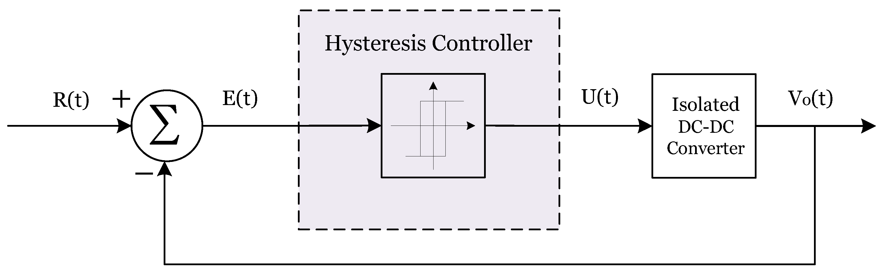
7.2. Hysteresis Controller (HC)

HCs in Figure 23 are easy to design and simple to implement. The voltage output is observed and modified in accordance with a predetermined threshold [132]. In addition, they offer superior sensitivity and are capable of responding quickly to dynamic changes in highly nonlinear systems. The HC current control method is widely used in DC–DC converters [133]. This control method offers a high level of accuracy and stability, thereby making it a popular choice for many applications. The HC control method uses an inner current loop to control the power transistor switching. Once the current exceeds a specific threshold, the power transistor is active. When the current decreases to a level below a specific threshold, the power transistor is turned off. This allows for a more precise control of transistor switching, which reduces switching losses and improves efficiency. However, it is important to note that these systems may experience unpredictable switching if not tuned correctly [133]. To overcome this drawback, the literature [134] provides various methods in order to maintain a constant switching frequency for HCs.

7.3. Sliding Mode Controller (SMC)

SMCs provide a robust control solution that is less affected by noise and disturbances. In SMCs, two components are required (as shown in Figure 24): the design of a sliding surface to ensure the system state remains steady at the origin after reaching the sliding surface, and the selection of a control law to guide the system state to the sliding surface. This type of controller is used because it can eliminate the Steady-State Error (SSE) and can reduce the Transient Response Time (TRT) [118]. It is also able to compensate for system parameter variations and non-linearities, thus making it a very efficient and reliable type of controller. However, high-frequency chattering can occur. In [135,136], several approaches to solving chattering problems were described. SMCs were utilised in [137,138] to regulate the output voltage and current for the bidirectional isolated Dual-Active-Bridge (DAB) DC–DC topology, while also providing a fast dynamic response to load fluctuations and robust parameter control.

7.4. Fuzzy Logic Controller (FLC)

FLCs are adaptive and can handle non-linear dynamics. They are also more energy-efficient than other types of controllers [139]. This type of controller is useful for applications where power regulation is needed, such as in solar power systems [139]. FLCs (Figure 25) are composed of three essential components: fuzzification, fuzzy logic rules, and defuzzification. Fuzzification is a crucial process where crisp input values are transformed into fuzzy linguistic values through the use of membership functions. Once this step is executed, the FLC proceeds to apply fuzzy logic rules to the fuzzy linguistic values, thus generating a fuzzy output value. The final step involves converting the fuzzy output value back into a crisp value via defuzzification. However, they are computationally intensive and difficult to implement. An FLC-based MPPT step-up push-pull topology is presented in [140]. Consequently, the suggested methodology offers several benefits in relation to its simplicity, accuracy, and low THD.

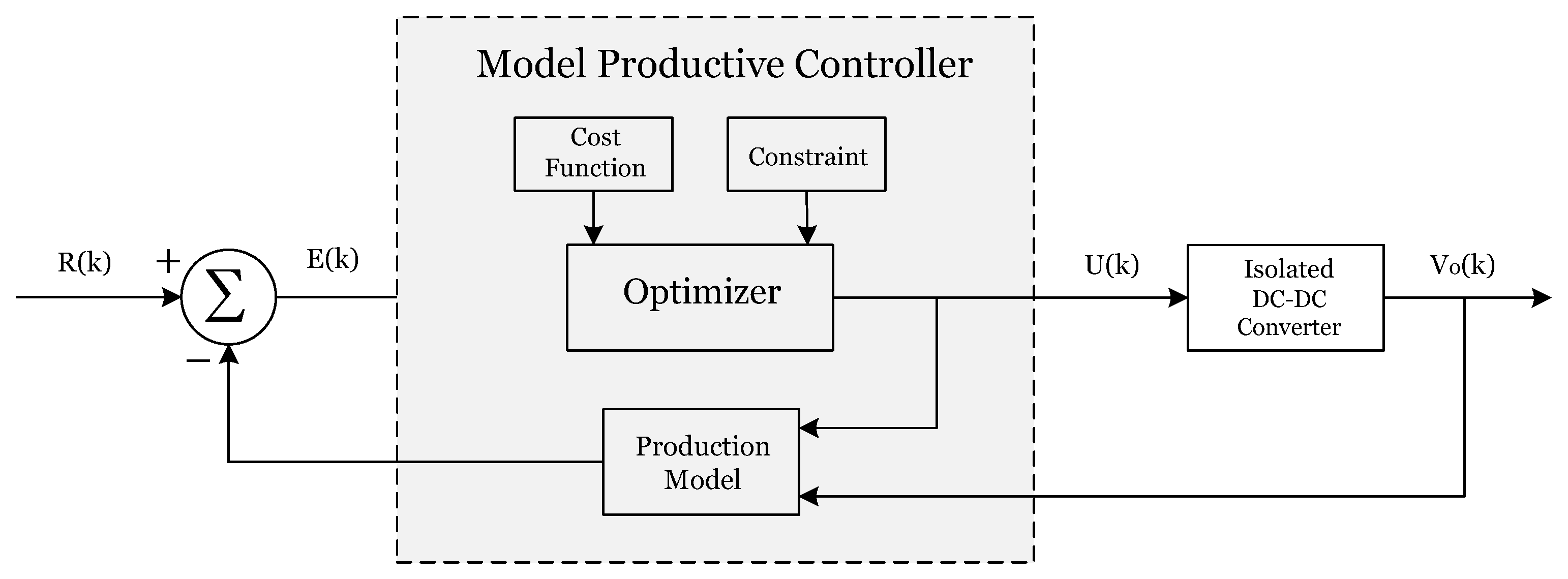
7.5. Model Predictive Controller (MPC)

MPCs are control systems that use a model of the process to predict future outputs, and thus optimise the control inputs to achieve desired outputs [16]. They use an optimisation algorithm to determine the best input sequence that will minimise a cost function. The resulting sequence of control actions is then executed by the controller, as seen in in Figure 26. Through using the MPC approach, a dual-bridge series resonant-isolated DC–DC converter was improved in [141]. The dynamicality of this system is greater than that of conventional PI control, and it is not sensitive to the parameters of the circuit. However, MPCs can be difficult to tune and may not always converge to the optimal solution. In some cases, it may be necessary to use trial and error to find the best set of tuning parameters. MPCs also require more computational resources than traditional PID controllers. Table 6 presents an overview of the advantages and disadvantages associated with the operation of control mechanisms.

8. Opportunities and Challenges

Selecting a suitable isolated DC–DC converter for a PV application will depend on specific requirements such as power rating, voltage conversion ratio, cost, size, efficiency, and reliability. Step-up isolated DC–DC constructions are limited by their design and the technology of the active and passive components they integrate. In order to achieve high power density and efficiency, isolated step-up converters need to reduce switch voltage stress, use fewer power components, and have a high step-up ratio. Currently, isolated DC–DC converters are the subject of intensive research and development. DC–DC converter sales in the global market are expected to increase from USD 9.9 billion in 2021 to USD 17.6 billion in 2026 at a compound annual growth rate of 12.1% [142]. Innovations in methods and topologies are needed to boost the conversion system while reducing cost, volume, and weight. Based on a detailed examination of all relevant topologies, it is evident that high-frequency transformers with complicated topologies are expensive and require more space and weight to be used in isolated DC–DC converters. Furthermore, conventional isolated DC–DC converters with transformers or coupled inductors suffer from several design defects, including leakage inductances that can cause voltage stress that damages circuit components. Having said this, stray capacitances of windings in the transformer generate high current spikes on the leading edge of the switch current waveform. To design isolated high-step-up DC–DC converters, parasitic components, including the transformer’s stray capacitance and leakage inductance, are essential. As a result of these difficulties, switching losses, low efficiency, and low reliability are increased.
Several methods were discussed in this article to address these effects, including the use of transformers or coupled inductors with resonant networks or snubber circuits. Both resonance networks and snubber circuits are used to control the switching transients that occur in isolated DC–DC converters. Resonance networks are designed to provide a resonant frequency to mitigate voltage and current stresses on the switching device, while snubber circuits are designed to absorb energy and improve the overall efficiency for the topology. In snubber circuits, using active snubbers provide better results in dealing with parasitic transformer components. It is able to reduce switching losses and improve the stability of the converter. In addition, transformers or coupled inductors can be used as isolation stages within VMC, SCC, and ZNC to reduce the turn ratio and switching loss while increasing the voltage gain and enhancing the performance. ZNCs can transfer power over a wide range of frequencies, allowing them to be used in various applications. However, the design of these converters is more complex than that of other step-up isolated DC–DC converters. A high voltage ratio is difficult to achieve with a ZNC due to its limited voltage-boosting capabilities. In particular, SC and VM can increase the voltage gain of a converter to a level beyond what is achievable with a ZNC, which makes them the preferred choice for most applications. SCC approaches have recently attracted substantial interest due to their lack of inductive components. This technique may provide the capability of generating higher power densities with a smaller form factor. However, capacitors are subjected to high current stresses, conduction losses, and input current pulsations. Even though this method has several drawbacks, it is nonetheless widely used. In contrast, VMCs have been demonstrated to increase step-up capabilities in various power electronic applications. In light of the extensive reviews presented in this article, the VMC approach is more suitable than other step-up techniques from the perspective of simplicity and performance. Also, it is widely used in isolated DC–DC converters. When these structures are added to the power stage of a converter, the gain ratio is adjusted. Apart from the many contributions of isolated DC–DC converters using VMC, they increase the cost and conversion efficiency. It will be necessary for future isolated converters utilising VMCs to keep the number of components in the converter as low as possible. This will keep costs low, make the converter smaller, and increase the power density.

9. Conclusions

In recent years, PV systems have become increasingly popular as a distributed energy-generating technology that is based on renewable energy resources. Isolated DC–DC topologies have been proven to be viable options for PV applications due to their higher power quality and ability to address safety concerns. In order to meet the growing demand for more efficient, reliable, and cost-effective systems, a rush of new research has been released to increase productivity and dependability while simultaneously reducing costs and lowering size. This paper provides a comprehensive overview of the various isolated DC–DC boost converter topologies and their features. This study examined and compared the different features of snubber circuits for isolated step-up DC–DC converters. The primary goal of most snubber circuits that have been developed over time is to reuse stored energy as a source or load, which can greatly improve converter efficiency. This paper also evaluated the use of nondissipative passive and active snubber types to eliminate the need for a snubber resistor, and their use in aiming to achieve high efficiency. In this study, several isolated DC–DC boost converters for a PV system were provided with ideas that can help increase converter voltage gain and efficiency. This paper also provides a comparison between several voltage-boost strategies for high-step isolated DC–DC converters. An in-depth analysis on all the relevant topologies revealed that the use of modifications are driven by a variety of aims, which include, but are not limited to, the following:
1.
Increasing voltage conversion ratios.
2.
Improving system efficiency.
3.
Reducing voltage stress among the components.
4.
Reducing complicity and improving system reliability.
There are several possible configurations for an isolated DC–DC architecture, including a flyback converter as a primary component with a low component count, a voltage multiplier cell to enhance voltage gain, and an active snubber to minimise switching losses by effectively recycling leakage inductance. By employing this approach, satisfactory results can be achieved, while at the same time ensuring a notable degree of efficacy and effectiveness for the converter. The objective of this research was to provide readers with a comprehensive understanding of isolated high-step-up converters, and to encourage further research in this area. The presented ideas and strategies for increasing converter voltage gain and efficiency can be applied to PV systems, as well as to other applications utilising isolated DC–DC topologies.

Funding

This research was supported in part by the UK Engineering and Physical Sciences Research Council (EPSRC) under Grant EP/T026162/1. For the purpose of open access, the author has applied a Creative Commons Attribution (CC BY) license to any Author Accepted Manuscript version arising.

Acknowledgments

H. Meshael would like to acknowledge the PhD scholarship provided by the Royal Saudi Cultural Bureau in London to carry out this research.

Conflicts of Interest

The authors declare no conflict of interest.

Abbreviations

The following abbreviations are used in this manuscript:
PVPhotovoltaic
RESsRenewable energy sources
SEPICSingle-ended primary inductor
CICoupled inductor
SISwitched inductor
SCSwitched capacitor
VMVoltage multiplier
PIDPotential-induced degradation
MPPTMaximum power point tracking
EMIElectromagnetic interference
IGBTInsulated-gate bipolar transistor
MOSFETMetal-oxide-semiconductor field effect transistor
ZVSZero-voltage switching
ZCSZero-current switching
CCMContinuous conduction mode
DCMDiscontinuous conduction mode
GaNGallium-nitride
LLCInductor–inductor–capacitor
PFMPulse-frequency modulation
PSMPhase-shift modulation
VTRVoltage tripler rectifier
VDRVoltage doubler rectifier
VFRVoltage fifth rectifier
RCDResistor–capacitor–diode
LCDInductor–capacitor–diode
VMCVoltage multiplier cell
SCCSwitched capacitor cell
ZNCImpedance network cell
qZSQuasi-impedance source
qSBQuasi-switched boost

Appendix A

To provide a further explanation of the cost calculations for the isolated DC–DC converters presented in Table 2, Table 3, Table 4 and Table 5, it is necessary to outline the component lists employed as representatives for all typologies to make a fair comparison. The switch (S) utilised was (IQE065N10NM5ATMA1), the diode (D) was (RURG80100-F085), the inductor (L) and the transformer (T) used (E 55/28/21 core), and the capacitor (C) was (68 μ F, 400 V). As an illustrative instance of the computations for the cost, consider the flyback converter shown in Figure 3a as an example:
C o s t = S + D + T + C = $ 2.96 + 2 × $ 6.19 + $ 4.51 + $ 4.84 = $ 24.69

References

  1. Way, R.; Ives, M.C.; Mealy, P.; Farmer, J.D. Empirically grounded technology forecasts and the energy transition. Joule 2022, 6, 2057–2082. [Google Scholar] [CrossRef]
  2. Moosavi, M.; Morya, A.; Toliyat, H.A. A low-cost soft-switching high step-up flyback converter with stacked output cells. In Proceedings of the 2017 IEEE Applied Power Electronics Conference and Exposition (APEC), Tampa, FL, USA, 26–30 March 2017; pp. 1700–1705. [Google Scholar]
  3. Gorji, S.A.; Sahebi, H.G.; Ektesabi, M.; Rad, A.B. Topologies and control schemes of bidirectional DC–DC power converters: An overview. IEEE Access 2019, 7, 117997–118019. [Google Scholar] [CrossRef]
  4. Schmitz, L.; Martins, D.C.; Coelho, R.F. Comprehensive conception of high step-up DC–DC converters with coupled inductor and voltage multipliers techniques. IEEE Trans. Circuits Syst. I Regul. Pap. 2020, 67, 2140–2151. [Google Scholar] [CrossRef]
  5. Imanlou, A.; Najmi, E.S.; Behkam, R.; Nazari-Heris, M.; Gharehpetian, G.B. A New High Voltage Gain Active Switched-Inductor Based High Step-up DC-DC Converter with Coupled-Inductor. IEEE Access 2023, 11, 56749–56765. [Google Scholar] [CrossRef]
  6. Gholizadeh, H.; Ben-Brahim, L. A new non-isolated high-gain single-switch DC–DC converter topology with a continuous input current. Electronics 2022, 11, 2900. [Google Scholar] [CrossRef]
  7. Farh, H.M.; Othman, M.F.; Eltamaly, A.M.; Al-Saud, M. Maximum power extraction from a partially shaded PV system using an interleaved boost converter. Energies 2018, 11, 2543. [Google Scholar] [CrossRef]
  8. Farh, H.M.; Eltamaly, A.M.; Al-Saud, M.S. Interleaved boost converter for global maximum power extraction from the photovoltaic system under partial shading. IET Renew. Power Gener. 2019, 13, 1232–1238. [Google Scholar] [CrossRef]
  9. Li, W.; He, X. Review of nonisolated high-step-up DC/DC converters in photovoltaic grid-connected applications. IEEE Trans. Ind. Electron. 2010, 58, 1239–1250. [Google Scholar] [CrossRef]
  10. Liang, T.J.; Lee, J.H.; Chen, S.M.; Chen, J.F.; Yang, L.S. Novel isolated high-step-up DC–DC converter with voltage lift. IEEE Trans. Ind. Electron. 2013, 60, 1483–1491. [Google Scholar] [CrossRef]
  11. Lee, J.; Kim, M.; Kim, S.; Choi, S. An isolated single-switch ZCS resonant converter with high step-up ratio. IEEE Trans. Power Electron. 2021, 36, 11555–11564. [Google Scholar] [CrossRef]
  12. Sutikno, T.; Samosir, A.S.; Aprilianto, R.A.; Purnama, H.S.; Arsadiando, W.; Padmanaban, S. Advanced DC–DC converter topologies for solar energy harvesting applications: A review. Clean Energy 2023, 7, 555–570. [Google Scholar] [CrossRef]
  13. Cheng, X.F.; Liu, C.; Wang, D.; Zhang, Y. State-of-the-art review on soft-switching technologies for non-isolated DC-DC converters. IEEE Access 2021, 9, 119235–119249. [Google Scholar] [CrossRef]
  14. Tofoli, F.L.; Pereira, D.d.C.; Josias de Paula, W.; Oliveira Junior, D.d.S. Survey on non-isolated high-voltage step-up dc–dc topologies based on the boost converter. IET Power Electron. 2015, 8, 2044–2057. [Google Scholar] [CrossRef]
  15. Mumtaz, F.; Yahaya, N.Z.; Meraj, S.T.; Singh, B.; Kannan, R.; Ibrahim, O. Review on non-isolated DC-DC converters and their control techniques for renewable energy applications. Ain Shams Eng. J. 2021, 12, 3747–3763. [Google Scholar] [CrossRef]
  16. Koç, Y.; Birbir, Y.; Bodur, H. Non-isolated high step-up DC/DC converters–An overview. Alex. Eng. J. 2022, 61, 1091–1132. [Google Scholar] [CrossRef]
  17. Amir, A.; Amir, A.; Che, H.S.; Elkhateb, A.; Abd Rahim, N. Comparative analysis of high voltage gain DC-DC converter topologies for photovoltaic systems. Renew. Energy 2019, 136, 1147–1163. [Google Scholar] [CrossRef]
  18. Alkhaldi, A.; Elkhateb, A.; Laverty, D. Voltage Lifting Techniques for Non-Isolated DC/DC Converters. Electronics 2023, 12, 718. [Google Scholar] [CrossRef]
  19. Jagadeesh, I.; Indragandhi, V. Comparative study of DC-DC converters for solar PV with microgrid applications. Energies 2022, 15, 7569. [Google Scholar] [CrossRef]
  20. Chub, A.; Vinnikov, D.; Blaabjerg, F.; Peng, F.Z. A review of galvanically isolated impedance-source DC–DC converters. IEEE Trans. Power Electron. 2015, 31, 2808–2828. [Google Scholar] [CrossRef]
  21. Chen, Y.; Xu, D. Review of soft-switching topologies for single-phase photovoltaic inverters. IEEE Trans. Power Electron. 2021, 37, 1926–1944. [Google Scholar] [CrossRef]
  22. Suryoatmojo, H.; Dilianto, I.; Mardiyanto, R.; Setijadi, E.; Riawan, D. Design and analysis of high gain modified SEPIC converter for photovoltaic applications. In Proceedings of the 2018 IEEE International Conference on Innovative Research and Development (ICIRD), Bangkok, Thailand, 11–12 May 2018; pp. 1–6. [Google Scholar]
  23. Priyadarshi, N.; Bhaskar, M.S.; Azam, F.; Singh, M.; Dhaked, D.K.; Taha, I.B.; Hussien, M.G. Performance evaluation of solar-PV-based non-isolated switched-inductor and switched-capacitor high-step-up cuk converter. Electronics 2022, 11, 1381. [Google Scholar] [CrossRef]
  24. Raj, A.; Praveen, R. Highly efficient DC-DC boost converter implemented with improved MPPT algorithm for utility level photovoltaic applications. Ain Shams Eng. J. 2022, 13, 101617. [Google Scholar] [CrossRef]
  25. Aghdam Meinagh, F.A.; Babaei, E.; Tarzamni, H.; Kolahian, P. Isolated high step-up switched-boost DC/DC converter with modified control method. IET Power Electron. 2019, 12, 3635–3645. [Google Scholar] [CrossRef]
  26. Jiang, S.; Cao, D.; Li, Y.; Peng, F.Z. Grid-connected boost-half-bridge photovoltaic microinverter system using repetitive current control and maximum power point tracking. IEEE Trans. Power Electron. 2012, 27, 4711–4722. [Google Scholar] [CrossRef]
  27. Bollipo, R.B.; Mikkili, S.; Bonthagorla, P.K. Hybrid, optimal, intelligent and classical PV MPPT techniques: A review. CSEE J. Power Energy Syst. 2020, 7, 9–33. [Google Scholar]
  28. Subudhi, B.; Pradhan, R. A comparative study on maximum power point tracking techniques for photovoltaic power systems. IEEE Trans. Sustain. Energy 2012, 4, 89–98. [Google Scholar] [CrossRef]
  29. Sutikno, T.; Subrata, A.C.; Elkhateb, A. Evaluation of fuzzy membership function effects for maximum power point tracking technique of photovoltaic system. IEEE Access 2021, 9, 109157–109165. [Google Scholar] [CrossRef]
  30. Li, X.; Wen, H.; Jiang, L.; Xiao, W.; Du, Y.; Zhao, C. An improved MPPT method for PV system with fast-converging speed and zero oscillation. IEEE Trans. Ind. Appl. 2016, 52, 5051–5064. [Google Scholar] [CrossRef]
  31. Cavalcanti, M.C.; Bradaschia, F.; do Nascimento, A.J.; Azevedo, G.M.; Barbosa, E.J. Hybrid maximum power point tracking technique for PV modules based on a double-diode model. IEEE Trans. Ind. Electron. 2020, 68, 8169–8181. [Google Scholar] [CrossRef]
  32. Yap, K.Y.; Sarimuthu, C.R.; Lim, J.M.Y. Artificial intelligence based MPPT techniques for solar power system: A review. J. Mod. Power Syst. Clean Energy 2020, 8, 1043–1059. [Google Scholar]
  33. Zaoskoufis, K.; Tatakis, E.C. Isolated ZVS-ZCS DC–DC High Step-Up Converter With Low-Ripple Input Current. IEEE J. Emerg. Sel. Top. Ind. Electron. 2021, 2, 464–480. [Google Scholar] [CrossRef]
  34. Beibei, R.; Dan, W.; Chengxiong, M.; Jun, Q.; Jiangang, Z. Analysis of full bridge DC-DC converter in power system. In Proceedings of the 2011 4th International Conference on Electric Utility Deregulation and Restructuring and Power Technologies (DRPT), Weihai, China, 6–9 July 2011; pp. 1242–1245. [Google Scholar]
  35. Forouzesh, M.; Siwakoti, Y.P.; Gorji, S.A.; Blaabjerg, F.; Lehman, B. Step-up DC–DC converters: A comprehensive review of voltage-boosting techniques, topologies, and applications. IEEE Trans. Power Electron. 2017, 32, 9143–9178. [Google Scholar] [CrossRef]
  36. Witulski, A.F. Introduction to modeling of transformers and coupled inductors. IEEE Trans. Power Electron. 1995, 10, 349–357. [Google Scholar] [CrossRef]
  37. Taneri, M.C.; Genc, N.; Mamizadeh, A. Analyzing and comparing of variable and constant switching frequency flyback DC-DC Converter. In Proceedings of the 2019 4th International Conference on Power Electronics and their Applications (ICPEA), Elazig, Turkey, 25–27 September 2019; pp. 1–5. [Google Scholar]
  38. Alhurayyis, I.; Elkhateb, A.; Morrow, J. Isolated and nonisolated DC-to-DC converters for medium-voltage DC networks: A review. IEEE J. Emerg. Sel. Top. Power Electron. 2020, 9, 7486–7500. [Google Scholar] [CrossRef]
  39. Li, W.; Liu, J.; Wu, J.; He, X. Design and analysis of isolated ZVT boost converters for high-efficiency and high-step-up applications. IEEE Trans. Power Electron. 2007, 22, 2363–2374. [Google Scholar] [CrossRef]
  40. Prabhakar, M.; Revathi B, S. High gain high power non-isolated DC-DC converter for renewable energy applications. In Proceedings of the 2014 IEEE 2nd International Conference on Electrical Energy Systems (ICEES), Chennai, India, 7–9 January 2014; pp. 229–234. [Google Scholar]
  41. Konar, S.; Saha, S.S. Efficient energy recovery and boosting the voltage gain of a soft-switched flyback converter. In Proceedings of the 2020 IEEE International Conference on Power Electronics, Drives and Energy Systems (PEDES), Jaipur, India, 16–19 December 2020; pp. 1–5. [Google Scholar]
  42. Hasan, R.; Hassan, W.; Xiao, W. A high gain flyback DC-DC converter for PV applications. In Proceedings of the 2020 IEEE REGION 10 CONFERENCE (TENCON), Osaka, Japan, 16–19 November 2020; pp. 522–526. [Google Scholar]
  43. Lee, S.W.; Do, H.L. Isolated High Step-Up Dual-Flyback DC–DC Converter with a Resonant Voltage Multiplier. Electr. Power Components Syst. 2020, 48, 871–880. [Google Scholar] [CrossRef]
  44. Ansari, S.A.; Moghani, J.S. A novel high voltage gain noncoupled inductor SEPIC converter. IEEE Trans. Ind. Electron. 2018, 66, 7099–7108. [Google Scholar] [CrossRef]
  45. Ahmad, S.; Tan, N.M.L.; Baharuddin, M.Z.; Buticchi, G. A high-performance isolated SEPIC converter for non-electrolytic LED lighting. IEEE Access 2021, 9, 149894–149905. [Google Scholar] [CrossRef]
  46. Yadav, A.; Verma, A. Sepic DC–DC converter: Review of different voltage boosting techniques and applications. In Proceedings of the 2020 2nd International Conference on Innovative Mechanisms for Industry Applications (ICIMIA), Bangalore, India, 5–7 March 2020; pp. 733–739. [Google Scholar]
  47. Somarowthu, P.R.R.; Saxena, S.K.; Mahajan, D.B. Isolated SEPIC converter with a novel voltage clamp circuit. In Proceedings of the 2018 IEEE International Conference on Power Electronics, Drives and Energy Systems (PEDES), Chennai, India, 18–21 December 2018; pp. 1–6. [Google Scholar]
  48. Ghasemi, A.; Adib, E.; Mohammadi, M.R. A new isolated SEPIC converter with coupled inductors for photovoltaic applications. In Proceedings of the 2011 19th Iranian Conference on Electrical Engineering, Tehran, Iran, 17–19 May 2011; pp. 1–5. [Google Scholar]
  49. Lee, S.W.; Do, H.L. Isolated SEPIC DC–DC converter with ripple-free input current and lossless snubber. IEEE Trans. Ind. Electron. 2017, 65, 1254–1262. [Google Scholar] [CrossRef]
  50. Lin, J.Y.; Lee, S.Y.; Ting, C.Y.; Syu, F.C. Active-clamp forward converter with lossless-snubber on secondary-side. IEEE Trans. Power Electron. 2018, 34, 7650–7661. [Google Scholar] [CrossRef]
  51. Xi, Y.; Jain, P.K. A forward converter topology with independently and precisely regulated multiple outputs. IEEE Trans. Power Electron. 2003, 18, 648–658. [Google Scholar]
  52. Abramovitz, A.; Cheng, T.; Smedley, K. Analysis and Design of Forward Converter With Energy Regenerative Snubber. IEEE Trans. Power Electron. 2010, 25, 667–676. [Google Scholar] [CrossRef]
  53. Gruner, V.F.; Horn, T.P.; Schmitz, L.; Martins, D.; Coelho, R. Forward-based high step-up DC–DC converter with input current sharing and output filter reduction: Design, modeling, and control. J. Control Autom. Electr. Syst. 2020, 31, 21–30. [Google Scholar] [CrossRef]
  54. Hwu, K.I.; Jiang, W.Z.; Chien, J. Isolated high voltage-boosting converter derived from forward converter. Int. J. Circuit Theory Appl. 2016, 44, 280–304. [Google Scholar] [CrossRef]
  55. Hwu, K.I.; Jiang, W.Z. An isolated high step-up converter with non-pulsating input current for renewable energy applications. J. Power Electron. 2016, 16, 1277–1287. [Google Scholar] [CrossRef]
  56. Montes, O.A.; Son, S.; Kim, S.; Seok, H.; Lee, J.S.; Kim, M. Forward-flyback resonant converter for high-efficient medium-power photovoltaic applications. In Proceedings of the 2017 IEEE Applied Power Electronics Conference and Exposition (APEC), Tampa, FL, USA, 26–30 March 2017; pp. 1223–1228. [Google Scholar]
  57. Hua, M.; Oian, B. A Hybrid Control Strategy for Forward flyback Converter with Improved Efficiency as an Interface to Low Voltage Renewable Sources. In Proceedings of the 2018 2nd IEEE Conference on Energy Internet and Energy System Integration (EI2), Beijing, China, 20–22 October 2018; pp. 1–5. [Google Scholar]
  58. Adhikari, N.; Singh, B.; Vyas, A.L.; Chandra, A.; Kamal-Al-Haddad. Analysis and design of isolated solar-PV energy generating system. In Proceedings of the 2011 IEEE Industry Applications Society Annual Meeting, Orlando, FL, USA, 9–13 October 2011; pp. 1–6. [Google Scholar]
  59. Whitaker, B.; Martin, D.; Cilio, E. Extending the operational limits of the push-pull converter with SiC devices and an active energy recovery clamp circuit. In Proceedings of the 2015 IEEE Applied Power Electronics Conference and Exposition (APEC), Charlotte, NC, USA, 15–19 March 2015; pp. 2033–2038. [Google Scholar]
  60. Ewerling, M.V.; Lazzarin, T.B.; Font, C.H.I. A three-level isolated dc-dc SEPIC converter with parallel-connected output. Int. J. Circuit Theory Appl. 2022, 51, 1224–1245. [Google Scholar] [CrossRef]
  61. Bilsalam, A.; Ekkaravarodome, C.; Chunkag, V.; Thounthong, P. Analyzing the Effect of Parasitic Capacitance in a Full-Bridge Class-D Current Source Rectifier on a High Step-Up Push–Pull Multiresonant Converter. Sustainability 2021, 13, 5477. [Google Scholar] [CrossRef]
  62. Lim, J.W.; Hassan, J.; Kim, M. Bidirectional soft switching push–pull resonant converter over wide range of battery voltages. IEEE Trans. Power Electron. 2021, 36, 12251–12267. [Google Scholar] [CrossRef]
  63. Xuewei, P.; Rathore, A.K. Current-fed soft-switching push–pull front-end converter-based bidirectional inverter for residential photovoltaic power system. IEEE Trans. Power Electron. 2014, 29, 6041–6051. [Google Scholar] [CrossRef]
  64. Nayanasiri, D.; Vilathgamuwa, D.M.; Maskell, D.L.; Beng, G.F.H. Soft-switching single inductor current-fed push-pull converter for PV applications. In Proceedings of the IECON 2014-40th Annual Conference of the IEEE Industrial Electronics Society, Dallas, TX, USA, 29 October–1 November 2014; pp. 5589–5594. [Google Scholar]
  65. Wang, C.; Li, M.; Ouyang, Z.; Wang, G. Resonant push–pull converter with flyback regulator for MHz high step-up power conversion. IEEE Trans. Ind. Electron. 2020, 68, 1178–1187. [Google Scholar] [CrossRef]
  66. Ali, K.; Raman, G.; Xiao, W.; Peng, J.C.H. A GaN-based High Step-Up Half-Bridge Resonant Converter for Interfacing PV Modules to DC Data Centers. In Proceedings of the 2019 IEEE 4th International Future Energy Electronics Conference (IFEEC), Singapore, 25–28 November 2019; pp. 1–8. [Google Scholar]
  67. Meghdad, T.; Jafar, M.; Bijan, A. High step-up current-fed ZVS dual half-bridge DC–DC converter for high-voltage applications. IET Power Electron. 2015, 8, 309–318. [Google Scholar] [CrossRef]
  68. York, B.; Yu, W.; Lai, J.S. An integrated boost resonant converter for photovoltaic applications. IEEE Trans. Power Electron. 2012, 28, 1199–1207. [Google Scholar] [CrossRef]
  69. Cao, D.; Jiang, S.; Peng, F.Z.; Li, Y. Low cost transformer isolated boost half-bridge micro-inverter for single-phase grid-connected photovoltaic system. In Proceedings of the 2012 Twenty-Seventh Annual IEEE Applied Power Electronics Conference and Exposition (APEC), Orlando, FL, USA, 5–9 February 2012; pp. 71–78. [Google Scholar]
  70. Lee, H.S.; Yun, J.J. Quasi-resonant voltage doubler with snubber capacitor for boost half-bridge DC–DC converter in photovoltaic micro-inverter. IEEE Trans. Power Electron. 2018, 34, 8377–8388. [Google Scholar] [CrossRef]
  71. Ikeda, S.; Kurokawa, F. Isolated and wide input ranged boost full bridge DC-DC converter with low loss active snubber. In Proceedings of the 2017 IEEE Energy Conversion Congress and Exposition (ECCE), Cincinnati, OH, USA, 1–5 October 2017; pp. 2213–2218. [Google Scholar]
  72. Zhang, Y.; Li, X.; Miu, Z.; Kundanam, K.; Liu, J.; Liu, Y.f. High step-up full bridge DC-DC converter with multi-cell diode-capacitor network. In Proceedings of the 2017 IEEE Applied Power Electronics Conference and Exposition (APEC), Tampa, FL, USA, 26–30 March 2017; pp. 157–163. [Google Scholar]
  73. Yao, Z.; Xu, J. An improved integrated boost full-bridge converter. In Proceedings of the 2016 IEEE Smart Energy Grid Engineering (SEGE), Oshawa, ON, Canada, 21–24 August 2016; pp. 191–195. [Google Scholar]
  74. Al-Atrash, H.; Batarseh, I. Boost-integrated phase-shift full-bridge converter for three-port interface. In Proceedings of the 2007 IEEE power electronics specialists conference, Orlando, FL, USA, 17–21 June 2007; pp. 2313–2321. [Google Scholar]
  75. Nguyen, T.T.; Cha, H.; Kim, H.G. Current-fed Quasi-Z-source full-bridge isolated DC–DC converter. IEEE Trans. Ind. Electron. 2020, 68, 12046–12057. [Google Scholar] [CrossRef]
  76. Alaql, F.; Batarseh, I. Review and comparison of resonant DC-DC converters for wide-output voltage range applications. In Proceedings of the 2020 IEEE Energy Conversion Congress and Exposition (ECCE), Detroit, MI, USA, 11–15 October 2020; pp. 1197–1203. [Google Scholar]
  77. Jiang, T.; Chen, X.; Zhang, J.; Wang, Y. Bidirectional LLC resonant converter for energy storage applications. In Proceedings of the 2013 Twenty-Eighth Annual IEEE Applied Power Electronics Conference and Exposition (APEC), Long Beach, CA, USA, 17–21 March 2013; pp. 1145–1151. [Google Scholar]
  78. Wei, Y.; Luo, Q.; Mantooth, A. A function decoupling partially isolated high voltage gain DC/DC converter for PV application. In Proceedings of the 2020 IEEE Transportation Electrification Conference & Expo (ITEC), Chicago, IL, USA, 23–26 June 2020; pp. 1–5. [Google Scholar]
  79. Wei, Y.; Luo, Q.; Mantooth, H.A. A Resonant Frequency Tracking Technique for LLC Converter-Based DC Transformers. IEEE J. Emerg. Sel. Top. Ind. Electron. 2021, 2, 579–590. [Google Scholar] [CrossRef]
  80. Zhou, J.; Ma, H. A new LLC converter with wide output voltage range and improved efficiency at medium or low output voltage. In Proceedings of the 2019 IEEE 28th International Symposium on Industrial Electronics (ISIE), Vancouver, BC, Canada, 12–14 June 2019; pp. 734–739. [Google Scholar]
  81. Alaql, F.; Batarseh, I. LLC resonant converter with reconfigurable voltage rectifier for wide input voltage applications. In Proceedings of the 2020 IEEE Energy Conversion Congress and Exposition (ECCE), Detroit, MI, USA, 11–15 October 2020; pp. 1191–1196. [Google Scholar]
  82. Seok, H.; Han, B.; Kwon, B.H.; Kim, M. High step-up resonant DC–DC converter with ripple-free input current for renewable energy systems. IEEE Trans. Ind. Electron. 2018, 65, 8543–8552. [Google Scholar] [CrossRef]
  83. Hua, G.; Leu, C.S.; Jiang, Y.; Lee, F.C. Novel zero-voltage-transition PWM converters. IEEE Trans. Power Electron. 1994, 9, 213–219. [Google Scholar]
  84. Bodur, H.; Bakan, A.F. A new zvt-zct-pwm dc-dc converter. IEEE Trans. Power Electron. 2004, 19, 676–684. [Google Scholar] [CrossRef]
  85. Han, S.K.; Yoon, H.K.; Moon, G.W.; Youn, M.J.; Kim, Y.H.; Lee, K.H. A new active clamping zero-voltage switching PWM current-fed half-bridge converter. IEEE Trans. Power Electron. 2005, 20, 1271–1279. [Google Scholar] [CrossRef]
  86. Hua, C.C.; Huang, C.Y. An active clamped two switch flyback Zeta converter with reduced switch voltage stress. In Proceedings of the 2019 2nd International Conference on High Voltage Engineering and Power Systems (ICHVEPS), Denpasar, Indonesia, 1–4 October 2019; pp. 1–5. [Google Scholar]
  87. Elkhateb, A.; Abd Rahim, N.; Selvaraj, J.; Williams, B.W. DC-to-DC converter with low input current ripple for maximum photovoltaic power extraction. IEEE Trans. Ind. Electron. 2014, 62, 2246–2256. [Google Scholar] [CrossRef]
  88. Vartak, C.; Abramovitz, A.; Smedley, K.M. Analysis and design of energy regenerative snubber for transformer isolated converters. IEEE Trans. Power Electron. 2014, 29, 6030–6040. [Google Scholar] [CrossRef]
  89. Ashish, M.; Anoop, P.; Lekshmi, K.R.; Ashraf Ali, V.K. Performance Analysis of A Current-fed Full Bridge Boost Converter with Passive and Active Clamp Circuit. In Proceedings of the 2021 International Conference on Communication, Control and Information Sciences (ICCISc), Idukki, India, 16–18 June 2021; Volume 1, pp. 1–5. [Google Scholar]
  90. Zhao, Q.; Lee, F.C. High-efficiency, high step-up DC-DC converters. IEEE Trans. Power Electron. 2003, 18, 65–73. [Google Scholar] [CrossRef]
  91. Wazarkar, S.N.; Rana, J.R. Comparative Study of Passive Regenerative and Dissipative Snubber Cells for Isolated SEPIC Converters. In Proceedings of the 2020 International Conference on Smart Innovations in Design, Environment, Management, Planning and Computing (ICSIDEMPC), Aurangabad, India, 30–31 October 2020; pp. 311–314. [Google Scholar]
  92. Lee, J.H.; Liang, T.J.; Chen, J.F. Isolated coupled-inductor-integrated DC–DC converter with nondissipative snubber for solar energy applications. IEEE Trans. Ind. Electron. 2013, 61, 3337–3348. [Google Scholar] [CrossRef]
  93. Chewale, M.A.; Wanjari, R.A.; Savakhande, V.B.; Sonawane, P.R. A review on isolated and non-isolated DC-DC converter for PV application. In Proceedings of the 2018 International Conference on Control, Power, Communication and Computing Technologies (ICCPCCT), Kannur, India, 23–24 March 2018; pp. 399–404. [Google Scholar]
  94. Nguyen, M.K.; Duong, T.D.; Lim, Y.C.; Kim, Y.J. Isolated boost DC–DC converter with three switches. IEEE Trans. Power Electron. 2017, 33, 1389–1398. [Google Scholar] [CrossRef]
  95. Evran, F.; Aydemir, M.T. Isolated high step-up DC–DC converter with low voltage stress. IEEE Trans. Power Electron. 2013, 29, 3591–3603. [Google Scholar] [CrossRef]
  96. Moraes, C.F.; Carati, E.G.; da Costa, J.P.; Cardoso, R.; de Oliveira Stein, C.M. Active-clamped zero-current switching current-fed half-bridge converter. IEEE Trans. Power Electron. 2019, 35, 7100–7109. [Google Scholar] [CrossRef]
  97. Dobakhshari, S.S.; Milimonfared, J.; Taheri, M.; Moradisizkoohi, H. A quasi-resonant current-fed converter with minimum switching losses. IEEE Trans. Power Electron. 2016, 32, 353–362. [Google Scholar] [CrossRef]
  98. Wu, T.F.; Chen, Y.C.; Yang, J.G.; Kuo, C.L. Isolated bidirectional full-bridge DC–DC converter with a flyback snubber. IEEE Trans. Power Electron. 2010, 25, 1915–1922. [Google Scholar]
  99. Zhiguo, Z.; Lin, Z. Analysis and design of isolated flyback voltage-multiplier converter for low-voltage input and high-voltage output applications. IET Power Electron. 2013, 6, 1100–1110. [Google Scholar] [CrossRef]
  100. Spiazzi, G.; Mattavelli, P.; Costabeber, A. High step-up ratio flyback converter with active clamp and voltage multiplier. IEEE Trans. Power Electron. 2011, 26, 3205–3214. [Google Scholar] [CrossRef]
  101. Shih Chieh, L. A multiphase Interleaved Boost Converter with Coupled Inductor for Fuel Cell APU Applications. Ph.D. Thesis, University of Nottingham, Nottingham, UK, 2018. [Google Scholar]
  102. Tseng, K.C.; Huang, H.S.; Cheng, C.A. Integrated boost-forward-flyback converter with high step-up for green energy power-conversion applications. IET Power Electron. 2021, 14, 27–37. [Google Scholar] [CrossRef]
  103. Kuo, P.; Liang, T.; Tseng, K.; Chen, J.; Chen, S. An isolated high step-up forward/flyback active-clamp converter with output voltage lift. In Proceedings of the 2010 IEEE Energy Conversion Congress and Exposition, Atlanta, GA, USA, 12–16 September 2010; pp. 542–548. [Google Scholar]
  104. Tseng, K.C.; Huang, C.C.; Cheng, C.A. A high step-up converter with voltage-multiplier modules for sustainable energy applications. IEEE J. Emerg. Sel. Top. Power Electron. 2015, 3, 1100–1108. [Google Scholar] [CrossRef]
  105. Alkhaldi, A.; Akbar, F.; Elkhateb, A.; Laverty, D. N-stage quadratic boost converter based on voltage lift technique and voltage multiplier. In Proceedings of the 11th International Conference on Power Electronics, Machines and Drives (PEMD 2022), Newcastle, UK, 21–23 June 2022. [Google Scholar]
  106. Luo, F.L. Luo-converters, voltage lift technique. In Proceedings of the PESC 98 Record. 29th Annual IEEE Power Electronics Specialists Conference (Cat. No. 98CH36196), Fukuoka, Japan, 22–22 May 1998; Volume 2, pp. 1783–1789. [Google Scholar]
  107. Salehi, S.M.; Hasanzadeh, S.; Shojaeian, H. A Dual Switch/Inductor Isolated High Voltage Gain based on Voltage Lift. In Proceedings of the 2021 12th Power Electronics, Drive Systems, and Technologies Conference (PEDSTC), Tabriz, Iran, 2–4 February 2021; pp. 1–5. [Google Scholar]
  108. Zhu, M.; Wang, T.; Luo, F.L. Analysis of voltage-lift-type boost converters. In Proceedings of the 2012 7th IEEE Conference on Industrial Electronics and Applications (ICIEA), Singapore, 18–20 July 2012; pp. 214–219. [Google Scholar]
  109. de Souza, A.F.; Tofoli, F.L.; Ribeiro, E.R. Switched capacitor DC-DC converters: A survey on the main topologies, design characteristics, and applications. Energies 2021, 14, 2231. [Google Scholar] [CrossRef]
  110. Kim, H.W.; Park, J.H. Isolated bidirectional switched-capacitor flyback converter. In Proceedings of the 2014 International Power Electronics and Application Conference and Exposition, Shanghai, China, 5–8 November 2014; pp. 279–284. [Google Scholar]
  111. Ioinovici, A. Switched-capacitor power electronics circuits. IEEE Circuits Syst. Mag. 2001, 1, 37–42. [Google Scholar] [CrossRef]
  112. Li, S.; Zheng, Y.; Wu, B.; Smedley, K.M. A family of resonant two-switch boosting switched-capacitor converter with ZVS operation and a wide line regulation range. IEEE Trans. Power Electron. 2017, 33, 448–459. [Google Scholar] [CrossRef]
  113. Li, S.; Xie, W.; Smedley, K.M. A family of an automatic interleaved Dickson switched-capacitor converter and its ZVS resonant configuration. IEEE Trans. Ind. Electron. 2018, 66, 255–264. [Google Scholar] [CrossRef]
  114. Li, S.; Zheng, Y.; Smedley, K.M. A family of step-up resonant switched-capacitor converter with a continuously adjustable conversion ratio. IEEE Trans. Power Electron. 2018, 34, 378–390. [Google Scholar] [CrossRef]
  115. Chung, H.S.H. Design and analysis of a switched-capacitor-based step-up DC/DC converter with continuous input current. IEEE Trans. Circuits Syst. I Fundam. Theory Appl. 1999, 46, 722–730. [Google Scholar] [CrossRef]
  116. Meshael, H.; Elkhateb, A.; Best, R. High Gain Isolated Switched-Boost DC-DC Converter for PV Application. In Proceedings of the 2023 IEEE International Conference on Environment and Electrical Engineering and 2023 IEEE Industrial and Commercial Power Systems Europe (EEEIC/I&CPS Europe), Madrid, Spain, 6–9 June 2023; pp. 1–6. [Google Scholar]
  117. Chen, J.F.; Zhang, C.M.; Wu, J.R.; Zhang, X.Q. Novel High Step-Up Isolated DC-DC Converter With Nondissipative Snubber and Switched-Capacitor Techniques. In Proceedings of the 2021 IEEE International Future Energy Electronics Conference (IFEEC), Taipei, Taiwan, 16–19 November 2021; pp. 1–6. [Google Scholar]
  118. Yang, L.; Yu, W.; Zhang, J. High voltage gain ratio isolated resonant switched-capacitor converter for sustainable energy. IEEE Access 2019, 7, 23055–23067. [Google Scholar] [CrossRef]
  119. Ramshanker, A.; Raglend, J.I. HFL High-gain Interleaved DC-DC Converter Operating in DCM and CRCM. In Proceedings of the 2022 IEEE 2nd International Conference on Sustainable Energy and Future Electric Transportation (SeFeT), Hyderabad, India, 4–6 August 2022; pp. 1–5. [Google Scholar]
  120. Guo, F.; Fu, L.; Zhang, X.; Yao, C.; Li, H.; Wang, J. A family of quasi-switched-capacitor circuit-based dual-input DC/DC converters for photovoltaic systems integrated with battery energy storage. IEEE Trans. Power Electron. 2016, 31, 8237–8246. [Google Scholar] [CrossRef]
  121. Fu, L.; Zhang, X.; Guo, F.; Wang, J. A phase shift controlled current-fed Quasi-Switched-Capacitor isolated dc/dc converter with GaN HEMTs for photovoltaic applications. In Proceedings of the 2015 IEEE Applied Power Electronics Conference and Exposition (APEC), Charlotte, NC, USA, 15–19 March 2015; pp. 191–198. [Google Scholar]
  122. Kim, D.H.; Kim, H.W.; Park, J.H.; Jeon, H.J. High efficiency high-step-up single-ended DC-DC converter with small output voltage ripple. J. Power Electron. 2015, 15, 1468–1479. [Google Scholar] [CrossRef]
  123. Siwakoti, Y.P.; Peng, F.Z.; Blaabjerg, F.; Loh, P.C.; Town, G.E. Impedance-source networks for electric power conversion part I: A topological review. IEEE Trans. Power Electron. 2014, 30, 699–716. [Google Scholar] [CrossRef]
  124. Torkan, A.; Ehsani, M. A novel nonisolated Z-source DC–DC converter for photovoltaic applications. IEEE Trans. Ind. Appl. 2018, 54, 4574–4583. [Google Scholar] [CrossRef]
  125. Fakhri, N.; Naderi, M.S.; Farkoush, S.G.; Khoshdel, A.; Aghili, S.; Choi, S.K.; Oh, S.R.; Rhee, S.B. Optimization of impedance-source galvanically isolated DC–DC converters with reduced number of switches. IEEE Access 2021, 10, 3835–3847. [Google Scholar] [CrossRef]
  126. Chub, A.; Vinnikov, D. Single-switch galvanically isolated quasi-Z-source DC-DC converter. In Proceedings of the 2015 IEEE 5th International Conference on Power Engineering, Energy and Electrical Drives (POWERENG), Riga, Latvia, 11–13 May 2015; pp. 582–586. [Google Scholar]
  127. Gorji, S.A.; Ektesabi, M.; Nguyen, T.N.; Zheng, J. Galvanically isolated switched-boost-based DC-DC converter. In Proceedings of the 2016 IEEE Energy Conversion Congress and Exposition (ECCE), Milwaukee, WI, USA, 18–22 September 2016; pp. 1–6. [Google Scholar]
  128. Paul, P.; Jose, B.R.; Shahana, T.K.; Abraham, C.; Mathew, J. High gain isolated quasi-switched boost converter embedded with switched capacitor cell. Electr. Power Components Syst. 2021, 49, 333–344. [Google Scholar] [CrossRef]
  129. Paul, P.; Jose, B.R.; Shahana, T.; Abraham, C.; Mathew, J. Isolated switched boost DC-DC converter with coupled inductor and transformer. In Proceedings of the TENCON 2019-2019 IEEE Region 10 Conference (TENCON), Kochi, India, 17–20 October 2019; pp. 1142–1147. [Google Scholar]
  130. Korompili, A.; Monti, A. Review of Modern Control Technologies for Voltage Regulation in DC/DC Converters of DC Microgrids. Energies 2023, 16, 4563. [Google Scholar] [CrossRef]
  131. Krommydas, K.F.; Alexandridis, A.T. Nonlinear analysis methods applied on grid-connected photovoltaic systems driven by power electronic converters. IEEE J. Emerg. Sel. Top. Power Electron. 2020, 8, 3293–3306. [Google Scholar] [CrossRef]
  132. Thi Kim Nga, T.; Park, S.M.; Park, Y.J.; Park, S.H.; Kim, S.; Van Cong Thuong, T.; Lee, M.; Hwang, K.C.; Yang, Y.; Lee, K.Y. A wide input range buck-boost DC–DC converter using hysteresis triple-mode control technique with peak efficiency of 94.8% for RF energy harvesting applications. Energies 2018, 11, 1618. [Google Scholar] [CrossRef]
  133. Ali Khan, M.Y.; Liu, H.; Yang, Z.; Yuan, X. A comprehensive review on grid connected photovoltaic inverters, their modulation techniques, and control strategies. Energies 2020, 13, 4185. [Google Scholar] [CrossRef]
  134. Syamala, L.; Sankar, D.; Makkar, S.E.; Jos, B.M.; Kallarackal, M. Hysteresis based quasi fixed frequency current control of single phase full bridge grid integrated voltage source inverter. Energies 2022, 15, 8112. [Google Scholar] [CrossRef]
  135. Komurcugil, H.; Biricik, S.; Bayhan, S.; Zhang, Z. Sliding mode control: Overview of its applications in power converters. IEEE Ind. Electron. Mag. 2020, 15, 40–49. [Google Scholar] [CrossRef]
  136. Mohd Zaihidee, F.; Mekhilef, S.; Mubin, M. Robust speed control of PMSM using sliding mode control (SMC)—A review. Energies 2019, 12, 1669. [Google Scholar] [CrossRef]
  137. Jeung, Y.C.; Lee, D.C. Voltage and current regulations of bidirectional isolated dual-active-bridge DC–DC converters based on a double-integral sliding mode control. IEEE Trans. Power Electron. 2018, 34, 6937–6946. [Google Scholar] [CrossRef]
  138. Tiwary, N.; Panda, A.K.; Narendra, A.; Lenka, R.K. A robust voltage control of DAB converter with super-twisting sliding mode approach. IEEE J. Emerg. Sel. Top. Ind. Electron. 2022, 4, 288–298. [Google Scholar] [CrossRef]
  139. Giurgi, G.I.; Szolga, L.A.; Giurgi, D.V. Benefits of fuzzy logic on MPPT and PI controllers in the chain of photovoltaic control systems. Appl. Sci. 2022, 12, 2318. [Google Scholar] [CrossRef]
  140. Hassan, T.u.; Abbassi, R.; Jerbi, H.; Mehmood, K.; Tahir, M.F.; Cheema, K.M.; Elavarasan, R.M.; Ali, F.; Khan, I.A. A novel algorithm for MPPT of an isolated PV system using push pull converter with fuzzy logic controller. Energies 2020, 13, 4007. [Google Scholar] [CrossRef]
  141. Song, W.; Zhong, M.; Deng, Y.; Yin, S.; Yu, B. Model Predictive Power Control for Bidirectional Series Resonant Isolated DC–DC Converters With Steady-State and Dynamic Performance Optimization. IEEE J. Emerg. Sel. Top. Ind. Electron. 2022, 3, 604–615. [Google Scholar] [CrossRef]
  142. Insights, F.B. DC-DC Converter Market Size, Share & COVID-19 Impact Analysis, by Type (Isolated and Non-Isolated), by Input Voltage (upto 40 V, 40 V to 100 V, 100 V to 500 v, and 500 V to 1000 v), by Output Voltage (upto 100 V, 100 V to 500 v, and 500 V to 1000 v), by End-User (Telecommunication, Automotive, Consumer Electronics, Energy & Power, Aerospace & Defense, Healthcare, and Others), and Regional Forecast, 2022–2029. Available online: https://www.fortunebusinessinsights.com/dc-dc-converter-market-106558 (accessed on 10 January 2023).
Figure 1. DC-DC Converter Classifications.
Electronics 12 03913 g001
Figure 2. General Structure of a High Step-Up Isolated DC–DC Converter for PV Systems.
Electronics 12 03913 g002
Figure 3. Coupled Inductor-Based Converters. (a) Conventional flyback converter and (b) conventional isolated SEPIC converter.
Electronics 12 03913 g003
Figure 4. Flyback Converters. (a) Isolated high step-up dual flyback topology ( 1   k W ) and (b) isolated high step-up dual-flyback topology using VM ( 120   W ).
Electronics 12 03913 g004
Figure 5. Isolated SEPIC Converters. (a) Isolated high step-up SEPIC topology using coupled inductors ( 530   W ), and (b) isolated high step-up SEPIC topology with a lossless snubber ( 100   W ).
Electronics 12 03913 g005
Figure 6. Transformer-Based Converter. (a) Conventional forward converter, (b) conventional push-pull converter, (c) conventional half-bridge converter, and (d) conventional full-bridge converter.
Electronics 12 03913 g006
Figure 7. Forward Converter Topologies. (a) Isolated high step-up DC–DC converter based on the forward topology with input current sharing ( 1   k W ), and (b) isolated high step-up forward topology ( 100   W ).
Electronics 12 03913 g007
Figure 8. Push-Pull Converter Topologies. (a) Isolated high step-up current-fed push-pull front-end topology ( 250   W ), and (b) isolated high step-up current-fed resonant push-pull topology ( 100   W 400   W ).
Electronics 12 03913 g008
Figure 9. Half-Bridge Converter Topologies. (a) Isolated high step-up CF dual half-bridge topology ( 1   k W ), and (b) isolated high step-up half-bridge topology with voltage doubler ( 300   W ).
Electronics 12 03913 g009
Figure 10. Full-Bridge Converter Topologies. (a) Isolated high step-up boost full-bridge topology ( 450   W ), and (b) isolated high step-up CF full-bridge topology with a quasi-Z-source network ( 1   k W ).
Electronics 12 03913 g010
Figure 11. Resonant Converter Topologies. (a) Isolated high step-up LLC topology based on a reconfigurable rectifier ( 250   W ), and (b) isolated high step-up resonant topology with the ripple-free input current ( 600   W ).
Electronics 12 03913 g011
Figure 12. Passive Snubber Circuits. (a) Isolated high step-up full-bridge boost topology using a passive RCD snubber ( 2   k W ), and (b) isolated high step-up coupled inductor topology with a nondissipative LCD snubber ( 200   W ).
Electronics 12 03913 g012
Figure 13. Active Snubber Circuits. (a) Isolated high step-up active clamp flyback converter ( 300   W ), and (b) isolated high step-up forward–flyback Converter (FFC) using the active clamp ( 800   W ).
Electronics 12 03913 g013
Figure 14. Circuits Based on Step-up Techniques. (a) Voltage multiplier (VM) cell. (b) Switched capacitor (SC) cell. (c) Impedance network (ZN) cell.
Electronics 12 03913 g014
Figure 15. VMC Circuits. (a) Isolated high-step-up topology with VLs ( 800   W ), and (b) isolated high step-up topology with VMs ( 500   W ).
Electronics 12 03913 g015
Figure 16. SCC Circuits. (a) Isolated high-step-up two-switch resonant switched-capacitor topology ( 500   W ), and (b) isolated high-step-up current-fed half-bridge quasi-switched capacitors ( 420   W ).
Electronics 12 03913 g016
Figure 17. ZSN Circuits. (a) Isolated high-step-up Z-source topology ( 200   W ), and (b) isolated high-step-up quasi-switched boost topology ( 250   W ).
Electronics 12 03913 g017
Figure 18. Converter Comparison. (a) Voltage Conversion Ratio (G) vs. Duty Cycle (D), and (b) Normalised Voltage Stress ( V s ) vs. Duty Cycle (D) ([10,39,47,67,75,89,102,104]).
Electronics 12 03913 g018
Figure 19. Number of Components in each Converter ([10,39,47,67,75,89,102,104]).
Electronics 12 03913 g019
Figure 20. Comparative Performance Analysis of each Converter. (a) [10] Figure 15a, (b) [39] Figure 4a, (c) [47] Figure 5a, (d) [67] Figure 9a, (e) [75] Figure 10b, (f) [89] Figure 12a, (g) [102] Figure 13b, and (h) [104] Figure 15a.
Electronics 12 03913 g020
Figure 21. Control Technique Classifications.
Electronics 12 03913 g021
Figure 22. PID Block Diagram.
Electronics 12 03913 g022
Figure 23. HC Block Diagram.
Electronics 12 03913 g023
Figure 24. SMC Block Diagram.
Electronics 12 03913 g024
Figure 25. FLC Block Diagram.
Electronics 12 03913 g025
Figure 26. MPC Block Diagram.
Electronics 12 03913 g026
Table 1. Main isolated DC-DC typology comparisons.
TopologiesMerits (+)Demerits (−)Sections
Flyback Converter
  • Low component count
  • Can be controlled easily
  • Cost-effective
  • Suitable for lower-power applications
  • Components under high voltage and current stress
  • Low efficiency rating
Section 3.1.1
Isolated SEPIC Converter
  • Utilises only one switch
  • Can be controlled easily
  • Low ripple current is present at the input
  • Suitable for lower-power applications
  • Range of power is limited
  • Switch is under high voltage stress
Section 3.1.2
Forward Converter
  • Low ripple voltage at the output
  • Suitable for low-to-medium power applications
  • Reset windings increase transformer complexity
  • Unsuitable for a step-up voltage
Section 3.2.1
Push-pull Converter
  • Suitable with applications involving fluctuating power
  • Operates at high switching frequencies
  • Devices have higher voltage ratings
  • Complex structure and control
Section 3.2.2
Half-Bridge Converter
  • Output voltage has a low ripple level
  • Operates at a wide input voltage range
  • High ripple current is present at the output
  • High number of elements
Section 3.2.3
Full-Bridge Converter
  • High density of power
  • Suitable for higher-power applications
  • Complex structure and control
  • Higher power dissipation
  • Overall cost is high
Section 3.2.4
Resonant Converter
  • Soft switching devices
  • High efficiency rating
  • Control design complexity for devices
  • Complex structure
  • High peak current is present
Section 3.2.5
Table 2. Comparison between flyback and isolated SEPIC topologies.
TopologiesComponent CountCost
(USD)
Voltage Conversion Ratio
of CCM (G)
Voltage Stress of
Main Switch (Vs)
Voltage Stress of
Output Diode ( V DO )
Switching
Performance
Input Current
Ripple
I/O Voltage
f s , P O
Duty Cycle
(D)
Efficiency
( η )
(+) Merits
(−) Demerits
LCDSTTotal
High Step-up Tow Switches
Flayback Converter [39]
Figure 4a
1424213USD 57.11 2 n ( 1 D ) V p v ( 1 D ) V o ZVSLow 40 V / 760 V
50 k Hz
1 k W
0.591%(+) High voltage gain
(+) Low voltage spike
(−) Complex structure and control
(−) High number of elements
High Step-up Dual
Flayback Converter [43]
Figure 4b
0441211USD 56.10 4 n ( 1 D ) 2 V p v V o 2 n V p v ZCS- 24 V / 200 V
50 k Hz
120 W
0.395.3%(+) Low reverse recovery losses
(+) Single switch
(+) Simple control circuit
(−) High conduction losses
High Step-up Isolated SEPIC
with Coupled Inductor [47]
Figure 5a
141219USD 40.49 D ( m + n ) ( 1 D ) V p v ( 1 D ) V o + ( m + n ) V p v ZVSHigh 50 V / 450 V
100 k Hz
530 W
0.693%(+) High voltage conversion ratio
(+) Simple structure
(−) High conduction losses
(−) High reverse recovery losses
High Step-up Isolated SEPIC
with Lossless Snubber [48]
Figure 5b
232119USD 43.39 n 2 D ( 1 D ) 2 V p v n 2 V p v + V o -Low 48 V / 200 V
50 k Hz
100 W
0.4193.8%(+) Low voltage spike
(+) Easy to control
(−) Low voltage gain
Note: L—inductor (including coupled inductors), C—capacitor (including input and output capacitors), D—diode, S—switch, and T—transformer.
Table 3. Property comparisons of the transformer-based topologies.
TopologiesComponent CountCost
(USD)
Voltage Conversion Ratio
of CCM (G)
Voltage Stress of
Main Switch ( V s )
Switching
Performance
Control
Parameters
I/O Voltage
f s , P o
Duty Cycle
(D)
Efficiency
( η )
(+) Merits
(−) Demerits
LCDSTTotal
High Step-up Forward Converter
with Input Current Sharing [52]
Figure 7a
1193 3 * 17USD 87.47 N n D --Voltage fed 30 V / 400 V
100 k Hz
1 k W
0.4585%(+) High voltage conversion ratio
(+) Low conduction losses
(−) High voltage stress on switches
(−) Low efficiency
High Step-up Forward Converter [53]
Figure 7b
2231210USD 49.25 D ( n 2 n 1 + n 3 n 1 D ( 1 D ) + n 4 n 1 ) 1 ( 1 D ) ZVSVoltage fed 12 V / 100 V
50 k Hz
100 W
0.6586.88%(+) Low voltage stress on switches
(−) Low efficiency
(−) Operate at high duty cycle.
(+) Low reverse recovery losses
(−) High conduction losses
High Step-up Push-Pull Front-End Converter [63]
Figure 8a
2408115USD 56.57 n ( 1 D ) V o n ZVCSCurrent fed 22 V 41 V / 200 V
100 k Hz
250 W
0.8092.7–94.8%((+) Low input current ripple
(+) Low conduction losses
(−) Operate at high duty cycle
(−) Complex control structure
High Step-up Resonant Push-Pull Converter [65]
Figure 8b
1554 2 * 17USD 80.52 n p p + n A C F D ( 1 D ) V p v V o n ZVSCurrent fed 24 V 32 V / 400 V
1 M Hz
100 W 400 W
0.4594–97.1%(+) High static gain
(+) High power density
(−) High number of power components
(−) Low reverse recovery losses
(−) High power switches
High Step-up Dual Half-Bridge Converter [67]
Figure 9a
1742216USD 78.09 2 n ( 1 D ) 1 ( 1 D ) V p v ZVSCurrent fed 50 V / 400 V
50 k Hz
1 k W
0.6596.52%(+) Low input current ripple
(+) Low voltage stress on switches
(−) High number of power components
High Step-up Half-Bridge Converter
with Voltage Doubler [70]
Figure 9b
1621212USD 57.91 n ( 1 a 2 a 3 ) ( 1 D a 3 a 1 ) V p v ( 1 D ) n I o 2 f s c s ZVSCurrent fed 13 V 50 V / 400 V
50 k Hz
300 W
0.5090%(+) High Voltage gain
(+) Low voltage stress on rectifier diodes
(−) Low efficiency
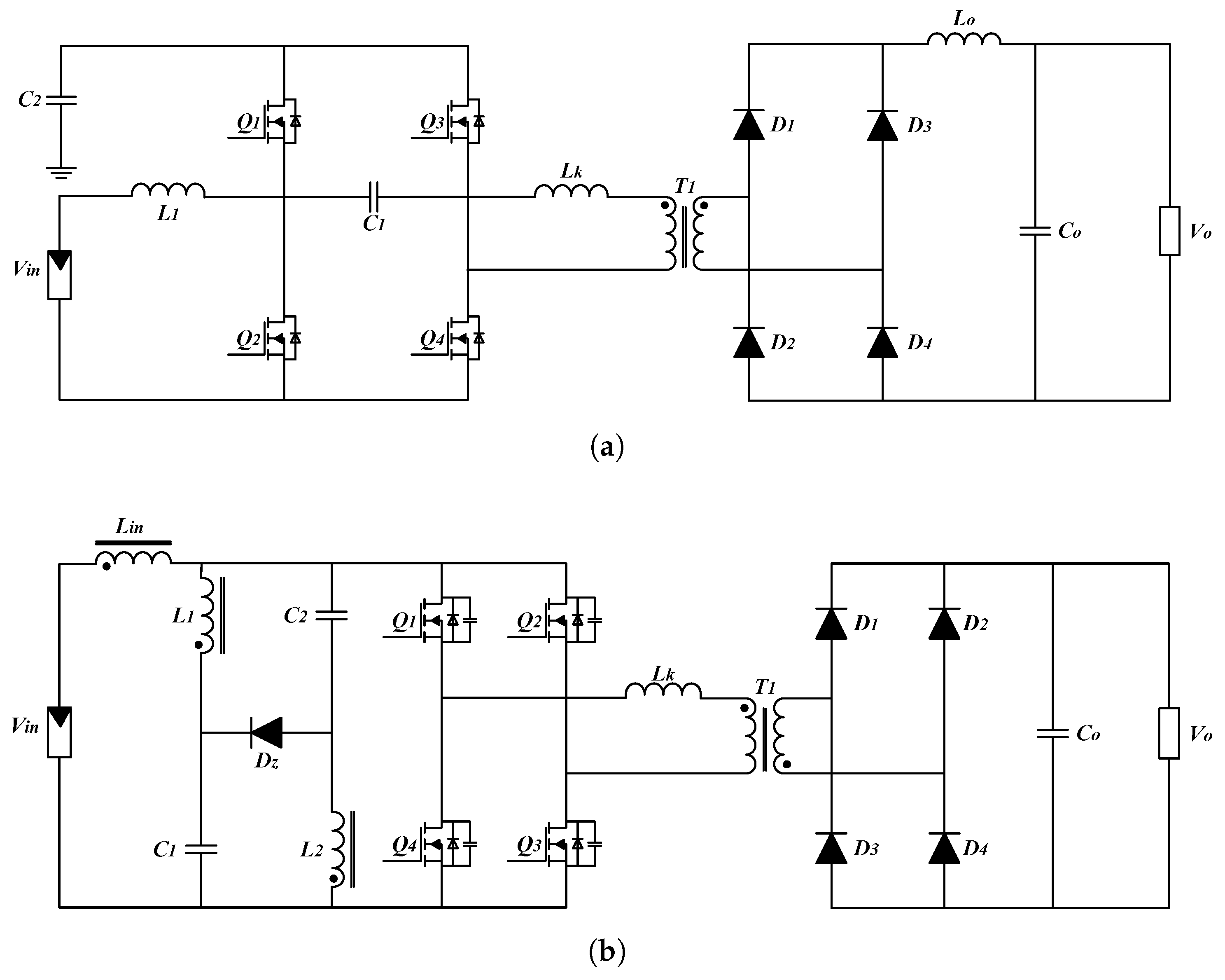
High Step-up Full-Bridge Converter [73]
Figure 10a
2344114USD 64.65 4 n D V p v ( 1 V o 4 n V p v ) -Current fed 20 V 70 V / 350 V
100 k Hz
450 W
0.55-(+) A low ripple in the input current
(+) Switches are decreased compared to
conventional full-bridge topology
(+) High voltage gain
(−) High reverse recovery losses
(−) High conduction losses
High Step-up Full-Bridge Converter
using a Quasi-Z Source [75]
Figure 10b
0354 2 * 14USD 66.33 n 2 ( 1 D ) 2 V p v -Current fed 33 V 60 V / 480 V
1 k W
0.25-0.7592.2–97.5%(+) High efficiency
(+) High voltage gain
(−) Complex control structure
(−) Switches are increased compared with
the traditional full-bridge topology.
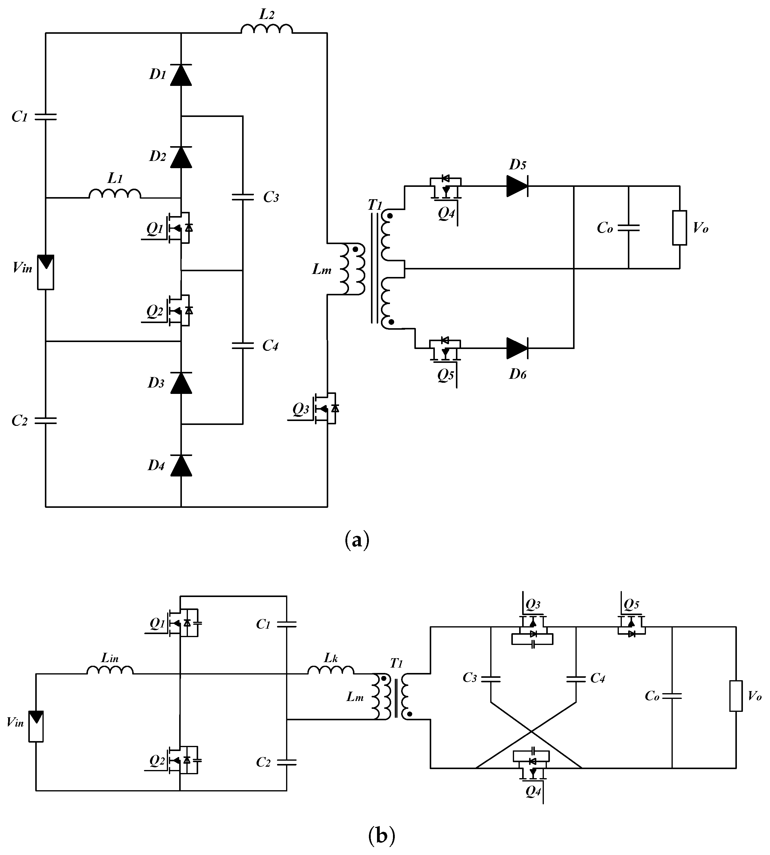
High Step-up LLC Converter
Based on a Reconfigurable Rectifier [81]
Figure 11a
1666120USD 92.96 T ( V c 1 o r c 4 ) n V p v -ZVCSVoltage fed 25 V 100 V / 500 V
69 k Hz 113 k Hz
250 W
-95–97.5%(+) High efficiency
(+) Operating within a wide variety
of input voltage levels.
(−) High number of components
(−) Complex control structure
High Step-up Resonant Converter
with The Ripple-Free Input Current [82]
Figure 11b
2406113USD 50.65 4 n N ( D s e c , Q ) -ZVCSCurrent fed 35 V 45 V / 380 V
50 k Hz
600 W
0.5096.6–97.3%(+) Low input current ripple
(+) High Voltage conversion ratio
(−) Complex control structure
(−) High voltage stress on secondary switches
Note—L: inductor (including coupled inductors), C: capacitor (including input and output capacitors), D: diode, S: switch, T: transformer, and *: three-winding transformer.
Table 4. Summary of snubber circuit topologies.
TopologiesSnubber CircuitComponent CountCost
(USD)
Voltage Conversion Ratio
of CCM (G)
Voltage Stress of
Main Switch (Vs)
Transformer
Turn Ratio
Control
Parameter
I/O Voltage
f s , P o
Duty Cycle
(D)
Efficiency
( η )
(+)Merit
(−) Demerits
LRCDSTTotal
High Step-up Full-Bridge
Boost Converter [89]
Figure 12a
Passive dissipative
RCD snubber
11118113USD 44.43 n ( 1 D ) V o n 1:6Current fed 48 V / 400 V
50 k Hz
2 k W
0.5089.8%(+) Low cost
(+) Simple structure
(+) Suitable for low power applications
(−) Less reliable for reducing voltage stress
(−) More passive components
High Step-up Coupled
Inductor Converter [92]
Figure 12b
Passive nondissipative
LCD snubber
10551113USD 67.13 n ( D + 1 ) ( 1 D ) V p v ( 1 D ) 1:3Voltage fed 24 V / 200 V
50 k Hz
200 W
0.4793.8%
High Step-up
Flyback converter [100]
Figure 13a
Active clamp snubber00522110USD 47.01 n ( 1 D ) V p v ( 1 + M A C ) 1:5.4Voltage fed 35 V / 400 V
100 k Hz
300 W
0.5694%(+) High efficiency
(+) More reliable for reducing voltage stress
(+) Suitable for low and high-power applications
(−) High cost
(−) More power switches
(−) Complex controls
High Step-up
Forward-Flyback
Converter (FFC) [102]
Figure 13b
Active clamp snubber10433112USD 55.83 n ( 2 D ) ( 1 D ) 2 V p v ( 1 D ) 1:2Voltage fed 48 V / 400 V
50 k Hz
800 W
0.4594%
Note—L: inductor (including coupled inductors), R: resistor, C: capacitor (including input and output capacitors), D: diode, S: switch, and T: transformer.
Table 5. Performance comparison of the various techniques for boosting isolated DC–DC converters.
TopologiesComponent CountCost
(USD)
Voltage Conversion Ratio of
CCM (G)
Voltage Stress of
Main Switch(Vs)
Input Current Ripple
Operation Modes
Control
Parameter
I/O Voltage
f s , P o
Duty Cycle
(D)
Efficiency
( η )
(+) Merits
(−) Dmerites
LCDSTTotal
High-Step-up Converter with Voltage
Lift [10]
Figure 15a
0452112USD 60.74 n ( 2 D ) ( 1 D ) v o n V p v 2 High
CCM, DCM
Voltage fed 24 V / 200 V
50 k Hz
800 W
0.4592.9%(+) Low voltage stresses
on power switches
(+) Simple control
(−) High conduction loss
High-Step-up Converter with Voltage
Multiplier [104]
Figure 15b
1452113USD 65.25 n ( 2 D ) ( 1 D ) 2 ( 1 D ) V o n ( 2 D ) Low
CCM
Current fed 40 V / 380 V
50 k Hz
500 W
0.5090.67%(+) High voltage
conversion ratio
(−) High reverse recovery
problem
High Step-up Resonant Switched Capacitor
Converter [118]
Figure 16a
2565 1 * 19USD 84.83 ( 2 V c ¯ ) ( T r f s q + D n 2 n 1 D ) -Normal
CCM, BCM, DCM
Current fed 24 V / 120 V
500 Hz 10 k Hz
500 W
0.5096.1%(−) High number of
components
(−) High reserve recovery
problem
(−) Low switching
frequency
High Step-up Half-Bridge
Quasi-Switched Capacitors
Converter [121]
Figure 16b
1505112USD 48.02--Normal
CCM
Current fed 46 V / 400 V
500 k Hz
420 W
0.5092.2%(+) High voltage gain
(−) High switching losses
(−) Complex controls
High Step-up Z-Source
Converter [125]
Figure 17a
2531112USD 59.26 n ( 1 2 D ) 2 V p v High
CCM
Voltage fed 50 V / 200 V
100 k Hz
200 W
0.2586.15%(+) Single switch
(+) Simple control
(−) Discontinuous input
current
(−) High reverse recovery
problem
High Step-up Quasi-Switched
Boost Converter [128]
Figure 17b
1453 1 * 12USD 68.21 4 n ( 1 2 D ) 4 V p v ( 1 2 D ) Low
CCM
Current fed 20 V – 40 V / 400 V
10 k Hz 20 k Hz
250 W
0.295.8%(+) Low energy losses
(−) The control system
is complex
(−) High reverse recovery
losses
Note—L: inductor (including coupled inductors), C: capacitor (including input and output capacitors), D: diode, S: switch, T: transformer, and *: three-winding transformer.
Table 6. Control technique comparisons.
TopologiesMerits (+)Demerits (−)References
Proportional
(P)
  • Easy to implement
  • Reduces rice time
  • Reduces steady-state error
  • High overshoot
  • Low stability
[3,130,133]
Proportional-integral
(PI)
  • Easy to implement
  • System accuracy is increased
  • Steady-state error is minimized
  • Low stability
  • Not suitable for rapid change
[3,16,133]
Proportional-integral-derivative
(PID)
  • High stability
  • Low overshoot
  • Fast response to disturbance
  • Complex structure
  • Sensitive to noises
[15,17,133]
Hysteresis controllers
(HC)
  • Adaptability to changing parameters
  • Rapid response
  • Easy to implement
  • Variation in switching frequency
  • Developing a filter to suppress switching harmonics is difficult
[132,133,134]
Sliding mode controllers
(SMC)
  • Response time is very fast
  • Inherent robustness
  • An effective method for dealing with disturbances
  • Chattering phenomena
  • Variable frequency
[135,136,137,138]
Fuzzy logic controllers
(FLC)
  • Use of mathematical models is unnecessary
  • Variable frequency
  • Magnitude of computation is significantly high
  • Switching frequency is variable
[15,140]
Model predictive controllers
(MPC)
  • Suitable for multi-input/multi-output
  • Rapid dynamic response
  • Intuitively manages system constraints.
  • Complex structure
  • Switching frequency is variable
[17,141]
Disclaimer/Publisher’s Note: The statements, opinions and data contained in all publications are solely those of the individual author(s) and contributor(s) and not of MDPI and/or the editor(s). MDPI and/or the editor(s) disclaim responsibility for any injury to people or property resulting from any ideas, methods, instructions or products referred to in the content.

