
IEC61131-3 Instruction List Language Processor for FPGAs

Department of Computer and Control Engineering, Rzeszów University of Technology, 35-959 Rzeszów, Poland
Electronics 2023, 12(19), 4052; https://doi.org/10.3390/electronics12194052
Submission received: 17 August 2023
/
Revised: 14 September 2023
/
Accepted: 25 September 2023
/
Published: 27 September 2023
Abstract
:This paper presents the architecture and field-programmable gate array (FPGA) implementation of a 32-bit central processing unit (CPU) dedicated to programmable logic controllers (PLCs). The CPU instruction set directly matches the instructions of the IEC 61131-3 standard Instruction List (IL) language. The designed IL processor is capable of handling 1-bit, 8-bit, 16-bit, and 32-bit data types. Apart from integer arithmetic operations, the IL processor also performs single precision floating-point operations included in the IEC 61131-3 IL language specification. It also directly performs instructions with a parenthesis modifier for all supported data types and facilitates the fast execution of a code containing Boolean expressions. This paper also presents the performance evaluation results of the developed IL processor. Although the IL processor executed the test algorithms substantially faster than industrial PLCs (e.g., Siemens S7-1200 and Fanux VersaMax), it turned out to be significantly slower than high-performance programmable automation controllers (PACs).
1. Introduction
For many years, programmable logic controllers (PLCs) have been a base for industrial automation due to their wide area of application, robustness, and easy programming using IEC 61131-3 languages [1,2]. Nowadays, the program execution speed of PLCs is becoming more important and, in some cases, might be considered a critical parameter for designed control systems. The microprocessors used in PLCs are, in some cases, general-purpose processors which might not be best suitable for the high program execution speed needed for the demanding applications of PLCs. Additionally, an instruction set of these general-purpose processors is not directly compatible with the programming languages defined by the IEC61131-3 standard. In particular, it refers to the assembler-like Instruction List (IL) language.
There are a number of research papers that have dealt with the development of dedicated central processing units (CPUs) that are intended to improve the speed of PLC program execution. These CPUs are often implemented and tested using hardware platforms based on field-programmable gate arrays (FPGAs). For example, one of the older papers [3] presented a special-purpose RISC microprocessor for programmable logic controllers. A specific instruction set optimized for the high-speed execution of bit instruction was developed for this microprocessor. The paper [4] presented the flow used in the design and construction of an application-specific, non-pipelined 8-bit microprocessor that would serve as the core of a PLC compatible with the IL programming language. The proposed microprocessor executed a specific set of instructions generated via the OpenPCS environment. The IP Core design of a microprocessor dedicated to PLCs, including a Boolean processing unit and a memory bit access interface, was portrayed in [5]. In [6], a PLC-dedicated processor consisting of a general processor and an application-specific instruction set processor was proposed. These two units were able to work concurrently, and the whole design was intended to improve the real-time performance of the PLC. Another work [7] presented an approach to the design and construction of central processing units for programmable logic controllers implemented in FPGAs. The CPU structure was based on bit–word architecture and two types of control data exchange methods: with and without handshaking. Additionally, a specific timer/counter hardware design solution was presented. In [8], the design process of a complete programmable logic controller implemented in FPGAs was discussed with particular emphasis on the central processing unit and memory map. An interesting design of a two-processor central processing unit dedicated to programmable logic controllers was depicted in [9]. This CPU was made up of a 1-bit (bit-type) processor and a 32-bit (word-type) processor. Both processors were developed as specialized structures capable of the execution of control routines developed in the Instruction List programming language, in line with the requirements of the EN 61131-3 standard. Another paper [10] proposed an Instruction List (IL) processor compatible with the IEC 61131-3 standards. A three-stage pipeline was applied so that each instruction was executed in a single machine cycle, providing high execution speed. In [11], the design and FPGA implementation of an IEC 61131-3 standard compatible Instruction List processor dedicated to PLC applications were described. A five-stage pipeline was proposed to increase the operation speed. Another IEC 61131-3 Instruction List processor was briefly described in [12]. In [13], an architecture based on an existing RISC-V processor targeted for the implementation of a PLC on FPGA was presented. The proposed solution included a conversion of the IEC 61131-3 Instruction List code into a processing system consisting of a RISC-V processor and peripherals. Another paper [14] depicted an IEC-61131-3-standard-compatible, three-stage instruction pipeline microprocessor implemented in FPGA. The processor had its own PLC-application-specific instruction set.
The current author’s previous work also includes the design of a multiprocessor programmable controller implemented in FPGAs [15] and programmed by means of the CPDev engineering environment [16]. The controller consisted of multiple identical CPUs, allowing a control program to be split into tasks executed in parallel and, hence, remarkably faster.
Only a few of the aforementioned papers, namely [9,10,11,12], directly considered the IEC 61131-3 IL instruction list as an instruction set for designed CPUs. Some of them (i.e., [11,12]) revealed very few details about the proposed architecture or its features. Additionally, in most cases, only a limited subset of IL instructions was implemented.
In this paper, the architecture of the 32-bit CPU for which the instruction set directly matches all instructions of the IEC61131-3 IL programming language, including instructions with the parenthesis modifier, is presented. The designed IL processor is capable of handling 1-bit, 8-bit, 16-bit, and 32-bit data types. It is also capable of performing all the logic and arithmetic operations, including single precision floating-point operations, constituted by the IEC61131-3 IL language standard. The presented processor is intended to become a faster successor of the CPU applied in [15]. The single CPU from [15] turned out to execute control programs considerably faster than some industrial PLCs (i.e., the Fanuc VeraMax and Siemens S7-1200) but slower than high-performance programmable automation controllers (PACs), particularly for logic control types of operations.
The instruction set of the CPU from [15] consisted of a relatively large number of rather complex instructions dedicated to software implementations of the CPDev virtual machine. It was neither targeted nor optimized for hardware implementation. The CPDev virtual machine instruction codes also had a variable length; therefore, multiple clock cycles were required to fetch a complete operation code with operands. The basic idea for a new CPU design was to simplify the instruction set and apply a reduced-instruction-set-computer-(RISC)-based accumulator machine architecture instead of complex instruction set computer (CISC) register machine architecture, where all instruction codes are fetched within a single clock cycle and as many as possible instructions are also executed within a single clock cycle. This should allow for a performance improvement of the CPU. Additionally, the use of ICE 61131-3 IL-language instructions as the CPU’s instruction list allows IL programs to be directly executed by the CPU for which every IL instruction has a machine code counterpart of this CPU.
2. Architecture
The proposed IL processor is, in fact, a kind of 32-bit microcontroller integrating many components of a programmable controller in a single FPGA chip. Its simplified architecture is presented in Figure 1.
The processor is based on the Harvard architecture, where data and program buses are separated. The data bus of the data memory is 32 bits wide, whereas the data bus of the program memory contains 40 bits. A relatively wide data bus for program memory allows all instruction codes with operands to be fetched within a single clock cycle, which is a characteristic feature of RISC processors.
The arithmetic logic unit (ALU) of the processor is fully 32-bit and performs all operations defined by the IEC 61131-3 Instruction List standard, including floating-point operations. The latter operations are supported by a dedicated floating-point unit, depicted in Figure 1. All operations results of the ALU block are directed to the 32-bit accumulator (ACC) registers, which are dubbed the current result (CR) in the IEC standard terminology. The contents of the ACC register are always the first operand of the ALU unit. The second operand comes from either the data memory (a variable) or program memory (a literal value). The MUX2 multiplexer provides the choice.
Apart from the ACC register, the processor also contains three other registers, namely the IX, IY, and T. The 4-bit T register stores the actual type of data stored in the accumulator. This could be one of the following types, directly corresponding with the IEC 61131-3 standard: 1-bit (BOOL), 8-bit (BYTE, SINT), 16-bit (WORD, INT), and 32-bit (DWORD, DINT, TIME, REAL). The two other registers are called index registers, and they can be used for an address calculation for the data memory. The final data memory address can be calculated as an addition of the IX (or IY) contents and a value coming directly from the instruction word. This feature facilitates a software implementation of IEC 61131-3 function block instances (the program code for all instances of a function block is common, but every single instance should have its own data structure, and hence, the IX or IY can act as a base address for these structures). This also allows the indirect addressing mode (the IX or IY can then be data pointers), which is an additional feature not included in the IEC 61131-3 IL standard. The choice between typical direct addressing and addressing with index registers is made by the MUX1 multiplexer. Additionally, the contents of the IY register can also be used as an address for the unconditional jump instruction. This feature allows, in turn, the most efficient implementation of state machines (no time is wasted in determining a value of the state variable).
Apart from the data and program memory, the architecture of the processor also includes the third type of memory, that is, the stack memory. This memory is organized as a last-in, first-out (LIFO) buffer controlled by the hardware. The value at the top of the stack is always available in the TOS register, which is not directly accessible via software. The stack memory is mainly used for the call of subroutine and the return from subroutine instructions, where the contents of the program counter (PC) are stored in this memory. The memory is also used for ALU operations with the parenthesis modifiers defined by the IEC 61131-3 IL standard. In this case, a single-stack memory location stores the contents of the ACC register (32 bits), the actual type (code) of operation for which the modifier is applied (4 bits), and the current data type for the ACC register (4 bits). Hence, the total word length of the stack memory is 40 bits.
All operations performed by the processor are controlled by the instruction decoder and the control unit (IDCU) block. This block is implemented as either a state machine, for instructions that require more than one clock cycle or a combinational one-hot decoder for single-cycle instructions. The IDCU block also controls the external input–output bus, which can be used as an interface for a global memory (according to the IEC61131-3 software model) or hardware function blocks, similar to the solution introduced in [15]. The external bus consists of a 16-bit address bus, a 32-bit input bus, a 32-bit output bus, and two 1-bit control signals (read and write). There are dedicated instructions that allow for reading and writing operations on the external bus.
The architecture of the processor portrayed in Figure 1 is very simplified. A somewhat more detailed part of the architecture involving the surrounding of the program counter and the stack memory is presented in Figure 2. The MUX4 multiplexer enables the choice of four register values to be stored in the stack memory, namely the accumulator, two index registers, and the incremented value of the program counter. The actual 40-bit value written to the stack memory is concatenated with the contents of the T register and the operation code for the operations with the parenthesis modifier. As Figure 2 suggests, the value of the program counter is determined by the MUX5 multiplexer. This value can be either the incremented value of the current contents of the PC register, the 20-bit address value coming from the top of the stack memory, the 20-bit value contained in the IY register, the direct address value coming from the instruction register, or the value that is an addition of the current value of the PC register and the accumulator value. The latter feature, along with the dedicated RETLA instruction (return from the subroutine and load the accumulator with the literal value), facilitates the reading of a table stored in the program memory. This is a very similar mechanism as implemented, for example, in some microcontrollers from Microchip.
The output of the MUX5 is connected to the set of D-type flip-flops that constitute the PC register and, simultaneously, to the address bus of the program memory. Since program memory is implemented as a synchronous BlockRAM memory inside the FPGA, a clock edge is required to read the value from the memory. The aforementioned way of connecting the program memory address bus ensures that the new instruction code is present in every clock cycle. This also means that jump instructions are performed within a single clock cycle. A similar solution was also implemented in [17].
Figure 3 reveals, in turn, more details related to the data memory section. Only a part of the architecture, including the data output section, is presented in this figure. In general, the data memory consists of five memory blocks. The first block is a small-capacity, 32-bit distributed RAM block (DRAM) with asynchronous read. The four remaining blocks are much-higher-capacity, 8-bit BlockRAM blocks (BRAM0…BRAM3). BlockRAM memory is synchronous memory that requires a clock edge for a reading operation. Therefore, an additional clock cycle is required to read an operand, and the IL processor machine cycle takes two clock cycles. If the operand comes from the distributed memory with asynchronous read, the machine cycle can be shorter and takes a single clock cycle. Hence, when the highest processing speed is required, the operands (variables) should be located in the DRAM block. However, for this version of the processor, the DRAM block can only handle 1-bit or 32-bit data, whereas the other blocks are able to process all data types.
The distributed memory and BlockRAM memory have different address ranges. The distributed memory is located in the high address space, whereas the BlockRAM memory is located in the low address space. The exact address ranges are selected via the address decoder block (ADDRDCD).
On account of the data memories’ organization and the fact that the IL processor is able to directly handle a few different data types (1-bit, 8-bit, 16-bit, and 32-bit), a number of multiplexers are needed in order to properly form the input operand for the ALU unit. Multiplexers MUX6…MUX9 and MUX13…MUX18 are responsible for the selection of a single bit within 32-bit words coming either from the BlockRAM or distributed memory. The multiplexers MUX10…MUX12 determine the order of the 8-bit, 16-bit, and 32-bit words, whereas MUX19…MUX22 finally form the 32-bit operand word (8-bit data from subsequent multiplexers are concatenated), which is delivered to the input of the MUX2 from Figure 1.
3. Instruction Set
Basically, The IL processor directly performs all instructions, including those with a parenthesis modifier, defined by the IEC 61131-3 standard. However, a few additional instructions have also been implemented that facilitate software development for programmable controllers. Therefore, some instructions’ mnemonics are slightly different than specified in the IEC 61131-3 standard. The complete instruction set of the IL processor with its exact counterparts from the IEC61131-3 IL standard is presented in Appendix A.
The general instruction format is presented in Figure 4. A program word is divided into a few sections, for which the exact boundaries depend on the instruction type. These sections include the operation code (OP), 32-bit literal field (s), 20-bit memory address (r), 4-bit data type field (t), 5-bit bit address field within a data memory word (b), and 1-bit destination bit (d). The latter bit determines whether the T register, indicating the type of currently processed data, should be updated with the “t” field contents. The bit address field allows a selection of a single bit within a 32-bit word. If 8-bit data are currently processed, then the two least significant bits of the “b” field determine which of the four bytes within a 32-bit word should be selected. A similar situation takes place when 16-bit data are currently processed—only the least significant bit of the “b” field indicates one of two 16-bit words within a 32-bit data word. Therefore, when a processor’s command with an operand coming from data memory is issued, four fields must be specified, namely “r”, “b”, “d”, and “t”. If the “d” bit is not set, then the actual data type (which also entails the interpretation of the “b” field contents) is determined by the contents of the T register. It is also worth noting that, when arithmetic or logic commands with index registers are used, the “r” field does not indicate the absolute data memory address but the offset from the base address contained in the index register.
Besides all instructions defined by the IEC 61131-3 standard, the processor also executes a few additional commands. These include the cumulative logical product (CAND and the corresponding CST instruction), basic stack operations (PUSH and POP), jump instructions with the address specified in the IY index register, the call-a-subroutine instruction with the address being a sum of the “r” field and the ACC register, return from a subroutine with a literal contained in the accumulator (RETLA), shift (SHL and SHR), and rotation (ROL and ROR) instructions, and input–output operations using the external bus (LDAIO and STIO).
The IL processor was developed with special attention paid to the fast execution of Boolean expressions, which was a relevant drawback of the processor from [15]. Therefore, the CAND instruction was developed. This instruction performs the same operation as the AND instruction and also updates the contents of an additional 1-bit register called CAR (cumulative and register). This register is not shown on the processor architecture in Figure 1. Every time the CAND instruction is performed, the new value of the CAR register is calculated as the logical sum of the current value of the CAR and the result of the AND operation. The corresponding CST instruction allows, in turn, rewriting of the CAR register contents to a specified memory location (the CAR register is also set to 0 simultaneously).
In order to illustrate how the CAND instruction may speed up calculations, let us consider the following Boolean expression, which might be part of excitation equations for some state machine (the one-hot encoding scheme has been applied):
where A, B, and C are the state variables, QT1 and QT2 are the outputs of IEC 61131-3 TON timers, X1 and X2 are input variables, and NB is the next state value for the B state variable. Table 1 shows three implementation versions of Equation (1) that use different instructions for the IL processor. The first version applies standard logical instructions (AND and OR) and requires an additional BOOL-type variable (TMP1). The second version exercises instructions with the parenthesis modifier (ORP and ANDNP). The EDO instruction evaluates the deferred operation, and it directly corresponds to the “)” IEC 61131-3 IL instruction. The third version, in turn, applies the CAND instruction. Every instruction in Table 1 might be executed via the IL processor within a single clock cycle. Therefore, the version with the CAND instruction takes the lowest number of clock cycles (9 cycles vs. 11/12 for version 2 and 13 for version 1) and is the fastest implementation of Equation (1).
NB = A ∗ X1 + B ∗ (X2 + QT1)’ + C ∗ QT2
Figure 5 shows a fragment of a behavioral simulation of the IL processor executing the code from Table 1, version 2 (the ISim simulator from Xilinx ISE 14.7 was used). The first two instructions of this code were omitted due to the better readability of the waveforms. This simulation illustrates that the operations with a parenthesis modifier are directly supported by the hardware. The values of a few internal registers, buses, and signals are presented in Figure 4, namely the clock line (CLK), program memory address bus (ADDRESS), program counter (_PC), instruction register (_INSTR), first input of the ALU (_ALU_IN1), accumulator (_ACC), stack pointer (_stack_ptr), top of the stack value (_TOS), address bus of data memory (_RAMADDR), “b” bit address field (_BFIELD), and distributed memory enable signal (_ED)—the ED output of the ADDRDCD block from Figure 3. All values from Figure 4 are given as hexadecimal. As can be seen, almost all instructions are executed within a single clock cycle. The contents of the program memory address bus are, in fact, the next value of the program counter, which usually is the PC register contents incremented by 1, unless a jump instruction is encountered (see also Figure 2). This allows for the current instruction to be fetched and, at the same clock cycle, for the instruction fetched in the previous cycle to be executed. Hence, two-stage pipelining was applied.
An exception to an instruction execution in a single clock cycle is a situation where two or more EDO instructions (or any other instructions that take the value from the stack memory) in a row are executed. In this case, the second (or any subsequent) instruction needs an additional clock cycle in order to read the value from the synchronous stack memory. This case is shown in waveforms in Figure 5 for the simulation time of 830 ns…870 ns.
It is also important to note that all variables for the simulation in Figure 5 were located in the distributed data memory that allows an asynchronous read operation. If the variables were located in the primary BlockRAM memory, the instructions that deal with these variables would also need two clock cycles. Such a case is presented as simulation waveforms in Figure 6. The simulated code is responsible for an invocation of the instance of the TON timer function block. The “ST T1_IN” instruction copies the accumulator contents to the specific location assigned for the IN input of the T1 instance of the TON function block. This location is in the BlockRAM memory at the address of 00010h (with the 0-bit field address); hence, the execution of this instruction takes two clock cycles. The next instruction loads the IX index register with the base address of the data structure for the T1 instance (000010h in this case). This instruction is executed in a single clock cycle. Similarly, the subsequent “CALL” instruction is also executed within a single clock cycle—on the next rising edge of the clock signal, an instruction is fetched directly from the address where the code of the TON function block is located (00080h in this case). The “LDAX IN” instruction reads the data memory location indicated by the sum of the IX register contents and the contents of the instruction address field. Therefore, in this case, the accumulator is loaded with the value of the previously assigned T1_IN variable. Similarly, the next instruction (“ANDNX PREV_IN”) also involves the IX register for the end-address calculation. The PREV_IN BOOL-type variable is located at the same absolute address as the T1_IN variable, but the bit address field for this instruction is different and accounts for 01h. The sequence of these latter two instructions, along with the jump instruction (“JMPCN C1”), determines whether the rising edge of the T1_IN variable has occurred. Since, for the “JMPCN” instruction, the jump is performed when the accumulator contains 0, and for this particular case from Figure 5, the accumulator contains 1, this means that the previously mentioned rising edge was detected and the jump instruction is not executed. Instead, the instruction from the next address is fetched, that is, the “LDA RTC” instruction. The 32-bit RTC variable located at the highest address of fffffh contains the system time, which can be used for time-measuring purposes.
The code beginning at the 00080h address is an example of a function block definition. The usage of the instructions dealing with the index registers effectively facilitates implementations of function block instances. The program code is common for all instances of a function block, but every instance has its own data structure, which can be pointed to by the index register. Hence, the code of a function block should apply the instructions with index registers in order to operate on the variables of a particular instance. If a function block calls another function block, then the current contents of the index register can be stored in the stack memory (the “PUSHX” and “PUSHY” instructions), and a new base address can be loaded to the index register. After returning from the second function block, the original value of the index register can be restored via the “POPX” (or “POPY”) instruction.
Most of the IL processor instructions are executed within either a single clock cycle or two clock cycles, depending on the type of operation and the type of memory used (BlockRAM or distributed RAM). However, floating-point arithmetic instructions require more clock cycles. For example, the addition/multiplication operation needs four clock cycles, whereas the division (which is also the slowest instruction) requires as many as eight clock cycles. It is worth noting that the IP cores performing these operations can be configured for a lower number of clock cycles, but it turned out that this compromises the maximum clock frequency of the implementation.
4. Implementation
The architecture of the IL processor was described using Verilog HDL. To verify the description, extensive simulations were carried out. The IL processor was also implemented and tested using the same FPGA board with a Xilinx Spartan-6 FPGA chip, which was designed and assembled for the multiprocessor programmable controller [15]. Apart from the mentioned board, the IL processor was also implemented using the Digilent Nexys 7 evaluation board. For comparison purposes, the HDL description of the IL processor was synthesized for a Xilinx Kintex-7 FPGA family as well. The implementation results, in terms of the utilization of the number of look-up tables (LUTs), flip-flops (FFs), and the maximum allowable clock frequency, are presented in Table 2.
Besides the FPGA resources portrayed in Table 2, the implementations also utilize 20 (for the Spartan-6 chip) or 18 (for Artix-7/Kintex-7 chips) digital signal processing blocks (DSPs). It is also important to note that, for the presented implementations, very modest memory resources were assigned. Namely, the BlockRAM data memory, distributed data memory, stack memory, and program memory had a 2K × 32-bit, 32 × 32-bit, 128 × 40-bit, and 1K × 40-bit subsequently. Therefore, the implementations also utilize 7 blocks of 16 Kbits and 3 blocks of 8 Kbit BlockRAM memories for the Spartan-6 chip or 8 blocks of 18 Kbit and 1 block of 36 Kbit BlockRAM memories for the other chips. However, since the IL processor exists as an HDL description, the size of all memories can easily be configured, depending on the actual needs and availability of resources for the selected FPGA chip.
It is worth noting that the resources utilization for the eight-core multiprocessor programmable controller from [15] amounted to 37,546 LUTs and 16,019 FFs (for the Spartan-6 chip). For a single processor core, this could be around 4695 LUTs and 2002 FFs. However, the entire implementation from [15] also included a few hardware function blocks, two access arbiters for common resources, and the communication module. Therefore, the number of utilized LUTs for a single-core processor from [15] should be less than one-eighth of the total LUT utilization but probably still slightly higher than for the presented IL processor.
Similarly, it turned out that the maximum allowable clock frequency is higher for the presented IL processor (64 MHz vs. 40 MHz for the implementation from [15]). Yet, the maximum clock frequency also depends on the applied FPGA chip. As the results in Table 2 indicate, for the Kintex-7 FPGA chip, this frequency can be significantly higher.
The comparison of the implementation results with other similar processors that consider the IL instruction set is not straightforward since different FPGAs with different architectures are applied. For example, one work [9] reported the utilization of 10,700 four-input LUTs and 16,675 FFs (the Virtex-4 FPGA chip was used). This seems to be a higher resource requirement than for the presented IL processor. However, for this IL processor, FPGA chips with six-input LUTs were used.
5. Performance Evaluation
For the performance evaluation of the IL processor, the same test algorithms were applied as for the multiprocessor controller [15], namely logic control (LC) and the crisp output calculation of a single class of the Takagi–Sugeno–Kang fuzzy-rule-based system (P1TS). The first algorithm performs the simple sequential control of an industrial process. It is described using a five-state machine diagram. The implementation of this algorithm involves five Boolean equations determined via the one-hot encoding scheme. One of these equations, in fact, is Equation (1). The second algorithm may be viewed as a special case of a Kolmogorov–Gabor polynomial [18] and can be applied, for example, to control mobile robots. Contrary to the LC test, the P1TS algorithm uses floating-point calculations.
The execution times of the test algorithms running on the IL processor are presented in Table 3. A few slightly different implementations of the LC algorithm were considered. The LC1 is the base implementation version for which all variables were located in the BlockRAM memory. This version implements Boolean equations in the same way as presented in Table 1, version 1. For the LC2, all state variables of the state machine were moved to the distributed memory, but the data structures of all TON timer instances were left in the BlockRAM memory. The LC3 version uses a parenthesis modifier for Boolean equation calculations (just like in Table 1, version 2). All variables were located identically as in the LC2 version. The LC4 is similar to LC3, but the data structures for TON timer instances were moved to distributed memory. For the LC5 version, the CAND instructions were applied (Table 1, version 3). All variables were located in the distributed memory. The LC6 version is similar to LC3, but all variables were also relocated to the distributed memory. The last version, LC7, uses CAND instructions. Additionally, all TON timer instances were implemented in hardware as hardware function blocks.
The P1TS algorithm was implemented as a series of functions. Each function called one or more of the other functions. Therefore, a relevant part of the algorithm implementation activity was arguments passing between functions. All variables for the P1TS implementation were located in the BlockRAM memory. Therefore, the implementation was slower than the fastest possible one, for which variables should be located in the distributed memory.
Calculation times were determined by both simulations and real hardware measurements. The exact number of clock cycles needed for the execution of a particular algorithm is easier and more precise to determine using the behavioral simulation of the IL processor description running a test algorithm. A few selected test algorithms were also executed using the IL processor implemented on the evaluation boards mentioned in Section 4. In this case, the code for a test algorithm was executed in the loop with 1000 iterations. After the loop was finished, the state of an external signal was inverted, and the loop was re-executed once again. The pulse time of the external signal was measured using a universal counter. Then, the calculation time of a test algorithm could be determined based on the pulse time and the number of loop iterations.
It is worth noting that the calculation times presented in Table 3 were given for the actual clock frequency as close as possible to the maximum allowable value, taking into account the frequency of the onboard oscillator and the features of the clocking resources of the particular FPGA chip.
As the results in Table 3 indicate, the slowest version of the LC algorithm implementation is the base version (LC1), in which all variables were located in the BlockRAM memory. Relocating these variables to the distributed memory (LC4) considerably reduced the number of clock cycles needed for algorithm calculation (218 cycles for LC1 vs. 119 for LC4). The usage of instructions with a parenthesis modifier did not bring about a relevant reduction in cycles (LC2 vs. LC3 or LC4 vs. LC6). The fastest version of a software implementation of the LC algorithm is definitely the version with the CAND instructions (LC5). However, a further reduction in the execution time can be achieved by applying hardware function blocks, which may implement a specific part of the algorithm via hardware (e.g., TON timer instances, as in the case of LC7).
It is worth noting that the LC algorithm executed using a single core of the multiprocessor controller [15] took 11.5 μs, while the Siemens S7-1200 and Fanuc VersaMax industrial PLCs needed 339.8 μs and 446.8 μs, respectively. The IL processor implemented in the same FPGA chip needs only 3.39 μs for the slowest realization of the algorithm and 1.60 μs for the fastest. This is a notable improvement. The same applies to the execution of the P1TS algorithm (117.3 μs for [15] vs. 27.67 μs for the IL processor). However, for [15], the algorithms were specified using the Structure Text (ST) language. Therefore, the effectiveness of the ST compiler may have also influenced the results.
Apart from the FPGA embedded controller described in [15] and the two aforementioned industrial PLCs, the performance of the IL processor was also compared with three arbitrarily chosen high-performance PAC controllers. The first two were Beckhoff CP6607 and CX5140. The popular Raspberry PI 4 module was applied as the hardware platform of the third controller. In this case, a CODESYS software environment (V3.5) and runtime were used for code preparation, debugging, and code execution on this hardware platform. In fact, the first PAC controller (Beckhoff CP6607) has also been considered in [15], but in that case, the test algorithms were written in the ST language. For this performance evaluation, all test algorithms were specified using the IEC 61131-3 IL language, and the same codes were applied for all tested PACs. Apart from the P1TS test algorithm, only two versions of the LC algorithm were involved, namely the base version (analogous to the LC4 version in Table 3) and the version with parenthesis modifiers (LC6).
The calculation time of all algorithms was measured using an IEC standard TON timer instance. After the activation of the timer, the particular test algorithm was executed in a loop for a certain number of iterations, and then the current time existing on the ET output of the TON timer instance was read. The final execution time of the algorithm was then calculated by dividing the latter time by the number of loop iterations.
This measurement method is not, in fact, as accurate as the one applied for the IL processor (the resolution of time measurement via the TON timer is low, and a few additional instructions are needed for the loop organization, which slightly affects the execution time), but it still might offer relevant information for speed comparison purposes. Additionally, due to the nature of the programmable controllers, the measured time fluctuates with every program cycle of the controller—in the table, only the shortest observed execution times are presented.
Apart from the absolute time, Table 4 also contains the equivalent number of cycle parameters (EC). The EC is calculated as the ratio between the execution time and the controller’s CPU clock period time. It can be treated as a counterpart of the number of clock cycles for the FPGA implementation of the IL processor.
The IL codes implementing the test algorithms were the exact counterparts of the codes applied for the IL processor, including a user-defined TON function block. Two versions of this block code were considered. The first version applies the TIME() standard library function to read a system time. The second one simply reads a DWORD-type variable instead of invoking the TIME() function—this is the exact behavior of the code dedicated to the IL processor (for the IL processor, reading a 32-bit variable from a specific memory location allows the reading of a system time value). Hence, two values of the algorithm execution time and the EC parameter, directly corresponding to these versions, are given in Table 4 for the latter two controllers.
As the results from Table 4 indicate, the execution time of the LC algorithm for the slowest Beckhoff controller is comparable to the time obtained by the IL processor implemented in FPGA chips in Table 3. However, the execution time of this algorithm delivered by the two other controllers is remarkably shorter (even by 17 times for the Raspberry/CODESYS platform in reference to the Spartan-6 implementation) than for the IL processor. It is worth noting that the execution time for these two controllers becomes notably longer (even by a few times) when the TIME() library function is applied for a time-lapse measurement. Similar dependencies can be observed for the P1TS algorithm. Its implementation on the latter two controllers from Table 4 is significantly faster (even by 9…27 times) than for the IL processor implemented on the FPGAs in Table 3. The opposite situation takes place for the slowest Beckhoff controller. In this case, the IL processor runs the P1TS algorithm considerably faster (by 7…12 times).
It is also worth noting that, for the Raspberry/CODESYS platform, the measurement of the P1TS execution time yields slightly different results for every several controller cycles—an increase from 1.06 μs to 1.98 μs was observed.
Considering the results in Table 4, it should be noted that the programmable controllers were clocked with a much higher frequency than the FPGA implementations of the IL processor (e.g., 1.91 GHz vs. 64.29 MHz). Therefore, a better indicator of the effectiveness of IL code execution might be the EC parameter. Taking into account this parameter, the IL processor turns out to be notably better in every single case in Table 4.
6. Conclusions
The developed IL processor turned out to be considerably faster than its predecessor from [15]. Therefore, the main design goal was achieved.
A significant increase in the execution speed of control programs containing Boolean expressions can be obtained using the cumulative AND instruction specially designed for the processor. Incorporating instructions with the parenthesis modifier into the instruction set of the IL processor also improves the execution speed of some control programs. However, a similar trend can be observed for industrial controllers that execute instructions with the parenthesis modifier.
As far as FPGA resource requirements and maximum clock frequency are concerned, the IL processor requires a lower number of resources than [15]. It also allows a higher clock frequency to be applied.
The relative execution speed of the IL processor, taking into account the clock frequency values, turned out to be considerably higher, even compared to high-performance industrial programmable controllers. This may be associated with the effective architecture of the IL processor. The other factor might be that the use of IL-language instructions as the instruction set of a CPU increases the execution speed of some types of control programs in comparison with general-purpose CPUs.
The absolute execution speed of the IL processor, although much higher than the industrial PLC controllers considered in [15], turned out to be significantly lower than the speed of high-performance PACs. This is related to a much lower clock frequency, which can be achieved for FPGA platforms. However, the FPGAs which were used for the implementation of the IL processor are more than a decade old and have not been manufactured with the newest 16 nm process technology (the 28 nm process technology has been applied for these FPGAs, in fact). Using newer FPGAs would probably decrease the speed difference between the IL processor and high-performance PAC controllers. Yet, obtaining a comparable speed seems difficult. The reconfiguration ability of FPGAs always comes at the price of longer internal delays than for ASIC technology, which limits the maximum clock frequency. To make, for example, the speed of the IL processor comparable with the Beckhoff CX5140 PAC controller, the FPGA implementation should be clocked with 476 MHz for the LC6 test algorithm and 647 MHz for the P1TS, respectively. However, the execution time of the P1TS test algorithm can be decreased relatively easily by means of relocating all variables to the distributed memory. Optimizing the critical path of the IL processor implementation and inserting some pipeline registers could also increase the maximum clock frequency but simultaneously increase the number of clock cycles needed for the execution of a particular operation, which might not entail a decrease in the overall execution time of a program. Additionally, the implementation of a combinational circuit consisting of a series connection of multiple multi-bit multiplexers from the data memory section (Figure 3) connected with the combinational circuit of the ALU unit requires a cascade of many LUTs. This entails a relatively long propagation delay time and substantially decreases the maximum clock frequency. Taking all these factors into account, the programmable controllers based on FPGA platforms with a single CPU might not be a more effective alternative to high-performance industrial PAC controllers, particularly in terms of the control program execution speed.
Funding
This project is financed by the Minister of Education and Science of the Republic of Poland within the “Regional Initiative of Excellence” program for years 2019–2023. Project number 027/RID/2018/19, amount granted 11 999 900 PLN.
Data Availability Statement
No additional data are provided.
Conflicts of Interest
The author declares no conflict of interest.
Appendix A
Below, a complete instruction set for the IL processor is given. The meanings of the subsequent symbols and registers are explained in Section 3. For all instructions involving the IX index register (the instruction mnemonic ends with the “X” character), there are also similar instructions dealing with the IY index registers. Their mnemonic ends, in turn, with the “Y” character.
| Mnemonic, Operand | IEC 61131-3 Counterpart | Description |
| LDIX s | IX<-s | |
| LDAL s.t.d | LD | ACC<-s, if d=1 then T<-t |
| LDA r.b.t.d | LD | ACC<-(r.b), if d=1 then T<-t |
| LDAN r.b.t.d | LDN | ACC<-NOT (r.b), if d=1 then T<-t |
| LDAX r.b.t.d | ACC<-(IX+r.b), if d=1 then T<-t | |
| LDANX r.b.t.d | ACC<-NOT (IX+r.b), if d=1 then T<-t | |
| LDAIO r | EXTERNAL_ADDR_BUS<-r, ACC<-EXTERNAL_DATA_BUS | |
| ST r.b | ST | (r.b)<-ACC |
| STN r.b | STN | (r.b.t)<-NOT ACC |
| STX r.b | (IX+r.b)<-ACC | |
| STNX r.b | (IX+r.b)<-NOT ACC | |
| STIO r | EXTERNAL_ADDR_BUS<-r, EXTERNAL_DATA_BUS<-ACC | |
| CST r.b | (r.b)<-CAR, CAR<-0 | |
| CSTN r.b | (r.b)<-NOT CAR, CAR<-0 | |
| CSTX r.b | (IX+r.b)<-CAR, CAR<-0 | |
| CSTNX r.b | (IX+r.b)<-NOT CAR, CAR<-0 | |
| S r.b | S | if ACC=1 then (r.b)<-1 |
| SX r.b | if ACC=1 then (IX+r.b)<-1 | |
| R r.b | R | if ACC=1 then (r.b)<-0 |
| RX r.b | if ACC=1 then (IX+r.b)<-0 | |
| JMP r | JMP | PC<-r |
| JMPC r | JMPC | if ACC=1 then PC<-r |
| JMPCN r | JMPCN | if ACC=0 then PC<-r |
| JMP IY | PC<-IY | |
| JMPC IY | if ACC=1 then PC<-IY | |
| JMPCN IY | if ACC=0 then PC<-r | |
| CALL r | CAL | TOS<-PC+1, PC<-r |
| CALLC r | CALC | if ACC=1 then TOS<-PC+1, PC<-r |
| CALLCN r | CALCN | if ACC=0 then TOS<-PC+1, PC<-r |
| CALLAA r | TOS<-PC+1, PC<-r | |
| RET | RET | PC<-TOS |
| RETC | RETC | if ACC=1 then PC<-TOS |
| RETCN | RETCN | if ACC=0 then PC<-TOS |
| RETLA s | PC<-TOS, ACC<-s | |
| PUSHA | TOS<-ACC | |
| PUSHX | TOS<-IX | |
| POPA | ACC<-TOS | |
| POPX | IX<-TOS | |
| AND s | AND | ACC<-ACC AND s |
| AND r.b.t.d | AND | ACC<-ACC AND (r.b), if d=1 then T<-t |
| ANDX r.b.t.d | AND | ACC<-ACC AND (IX+r.b), if d=1 then T<-t |
| ANDN r.b.t.d | ANDN | ACC<-ACC AND NOT (r.b), if d=1 then T<-t |
| ANDNX r.b.t.d | ACC<-ACC AND NOT (IX+r.b), if d=1 then T<-t | |
| ANDP r.b.t.d | AND( | TOS<-{ACC,”AND”}, ACC<-(r.b), if d=1 then T<-t |
| ANDPX r.b.t.d | TOS<-{ACC,”AND”}, ACC<-(IX+r.b), if d=1 then T<-t | |
| ANDNP r.b.t.d | ANDN( | TOS<-{ACC,”AND NOT”}, ACC<-(r.b), if d=1 then T<-t |
| ANDNPX r.b.t.d | TOS<-{ACC,”AND NOT”}, ACC<-(IX+r.b), if d=1 then T<-t | |
| CAND r.b | ACC<-ACC AND (r.b), CAR<-CAR OR ACC | |
| CANDX r.b | ACC<-ACC AND (IX+r.b), CAR<-CAR OR ACC | |
| OR s | OR | ACC<-OR AND s |
| OR r.b.t.d | OR | ACC<-ACC OR (r.b), if d=1 then T<-t |
| ORX r.b.t.d | OR | ACC<-ACC OR (IX+r.b), if d=1 then T<-t |
| ORN r.b.t.d | ORN | ACC<-ACC OR NOT (r.b), if d=1 then T<-t |
| ORNX r.b.t.d | ACC<-ACC OR NOT (IX+r.b), if d=1 then T<-t | |
| ORP r.b.t.d | OR( | TOS<-{ACC,”OR”}, ACC<-(r.b), if d=1 then T<-t |
| ORPX r.b.t.d | TOS<-{ACC,”OR”}, ACC<-(IX+r.b), if d=1 then T<-t | |
| ORNP r.b.t.d | ORN( | TOS<-{ACC,”OR NOT”}, ACC<-(r.b), if d=1 then T<-t |
| ORNPX r.b.t.d | TOS<-{ACC,”OR NOT”}, ACC<-(IX+r.b), if d=1 then T<-t | |
| XOR s | XOR | ACC<-ACC XOR s |
| XOR r.b.t.d | XOR | ACC<-ACC XOR (r.b), if d=1 then T<-t |
| XORX r.b.t.d | ACC<-ACC XOR (IX+r.b), if d=1 then T<-t | |
| XORN r.b.t.d | XORN | ACC<-ACC XOR NOT (r.b), if d=1 then T<-t |
| XORNX r.b.t.d | ACC<-ACC XOR NOT (IX+r.b), if d=1 then T<-t | |
| XORP r.b.t.d | XOR( | TOS<-{ACC,”XOR”}, ACC<-(r.b), if d=1 then T<-t |
| XORPX r.b.t.d | TOS<-{ACC,”XOR”}, ACC<-(IX+r.b), if d=1 then T<-t | |
| XORNP r.b.t.d | XORN( | TOS<-{ACC,”XOR NOT”}, ACC<-(r.b), if d=1 then T<-t |
| XORNPX r.b.t.d | TOS<-{ACC,”XOR NOT”}, ACC<-(IX+r.b), if d=1 then T<-t | |
| ADD s | ADD | ACC<-ACC + s |
| ADD r.b.t.d | ADD | ACC<-ACC + (r.b), if d=1 then T<-t |
| ADDX r.b.t.d | ACC<-ACC + (IX+r.b), if d=1 then T<-t | |
| ADDP r.b.t.d | ADD( | TOS<-{ACC,”+”}, ACC<-(r.b), if d=1 then T<-t |
| ADDPX r.b.t.d | TOS<-{ACC,”+”}, ACC<-(IX+r.b), if d=1 then T<-t | |
| SUB s | SUB | ACC<-ACC—s |
| SUB r.b.t.d | SUB | ACC<-ACC—(r.b), if d=1 then T<-t |
| SUBX r.b.t.d | SUB | ACC<-ACC—(IX+r.b), if d=1 then T<-t |
| SUBP r.b.t.d | SUB( | TOS<-{ACC,”-”}, ACC<-(r.b), if d=1 then T<-t |
| SUBPX r.b.t.d | TOS<-{ACC,”-”}, ACC<-(IX+r.b), if d=1 then T<-t | |
| MUL s | MUL | ACC<-ACC * s |
| MUL r.b.t.d | MUL | ACC<-ACC * (r.b), if d=1 then T<-t |
| MULX r.b.t.d | ACC<-ACC * (IX+r.b), if d=1 then T<-t | |
| MULP r.b.t.d | MUL( | TOS<-{ACC,”*”}, ACC<-(r.b), if d=1 then T<-t |
| MULPX r.b.t.d | TOS<-{ACC,”*”}, ACC<-(IX+r.b), if d=1 then T<-t | |
| DIV s | DIV | ACC<-ACC/s |
| DIV r.b.t.d | DIV | ACC<-ACC/(r.b), if d=1 then T<-t |
| DIVX r.b.t.d | ACC<-ACC/(IX+r.b), if d=1 then T<-t | |
| DIVP r.b.t.d | DIV( | TOS<-{ACC,”/”}, ACC<-(r.b), if d=1 then T<-t |
| DIVPX r.b.t.d | TOS<-{ACC,”/”}, ACC<-(IX+r.b), if d=1 then T<-t | |
| GT s | GT | if ACC > s then ACC<-1 else ACC<-0 |
| GT r.b | GT | if ACC > (r.b) then ACC<-1 else ACC<-0 |
| GTX r.b | GT | if ACC > (IX+r.b) then ACC<-1 else ACC<-0 |
| GTE s | GTE | if ACC >= s then ACC<-1 else ACC<-0 |
| GTE r.b | GTE | if ACC >= (r.b) then ACC<-1 else ACC<-0 |
| GTEX r.b | if ACC >= (IX+r.b) then ACC<-1 else ACC<-0 | |
| EQ s | EQ | if ACC = s then ACC<-1 else ACC<-0 |
| EQ r.b | EQ | if ACC = (r.b) then ACC<-1 else ACC<-0 |
| EQX r.b | if ACC = (IX+r.b) then ACC<-1 else ACC<-0 | |
| NE s | NE | if ACC <> s then ACC<-1 else ACC<-0 |
| NE r.b | NE | if ACC <> (r.b) then ACC<-1 else ACC<-0 |
| NEX r.b | if ACC <> (IX+r.b) then ACC<-1 else ACC<-0 | |
| LT s | LT | if ACC < s then ACC<-1 else ACC<-0 |
| LT r.b | LT | if ACC < (r.b) then ACC<-1 else ACC<-0 |
| LTX r.b | if ACC < (IX+r.b) then ACC<-1 else ACC<-0 | |
| LTE s | LTE | if ACC <= s then ACC<-1 else ACC<-0 |
| LTE r.b | LTE | if ACC <= (r.b) then ACC<-1 else ACC<-0 |
| LTEX r.b | if ACC <= (IX+r.b) then ACC<-1 else ACC<-0 | |
| EDO | ) | {TMPA,OP}<-TOS, ACC<-TMPA OP A |
| SHLA | ACC<- SHIFT_LEFT ACC | |
| SHL r.b | ACC<- SHIFT_LEFT (r.b) | |
| SHLX r.b | ACC<- SHIFT_LEFT (IX+r.b) | |
| SHRA | ACC<- SHIFT_RIGHT ACC | |
| SHR r.b | ACC<- SHIFT_RIGHT (r.b) | |
| SHRX r.b | ACC<- SHIFT_RIGHT (IX+r.b) | |
| ROLA | ACC<- ROTATE_LEFT ACC | |
| ROL r.b | ACC<- ROTATE_LEFT (r.b) | |
| ROLX r.b | ACC<- ROTATE_LEFT (IX+r.b) | |
| RORA | ACC<- ROTATE_RIGHT ACC | |
| ROR r.b | ACC<- ROTATE_RIGHT (r.b) | |
| RORX r.b | ACC<- ROTATE_RIGHT (IX+r.b) |
References
- IEC 61131-3; International Standard Edition 3.0. International Electrotechnical Commission: Geneva, Switzerland, 2013.
- John, K.H.; Tiegelkamp, M. IEC 61131-3: Programming Industrial Automation Systems; Springer: Berlin/Heidelberg, Germany, 2010. [Google Scholar]
- Rho, G.S.; Koo, K.H.; Chang, N.; Park, J.; Kim, J.G.; Kwon, W.H. Implementation of a RISC microprocessor for programmable logic controllers. Microprocess. Microsyst. 1995, 19, 599–608. [Google Scholar] [CrossRef]
- Snaider Carrillo, L.; Agenor Polo, Z.; Mario Esmeral, P. Design and Implementation of an Embedded Microprocessor Compatible with IL Language in Accordance to the Norm IEC 61131-3. In Proceedings of the International Conference on Reconfigurable Computing and FPGAs (ReConFig), Puebla, Mexico, 28–30 September 2005. [Google Scholar]
- Xu, M.; Ran, F.; Chen, Z.; Kang, S.; Li, R. IP Core Design of PLC Microprocessor with Boolean Module. In Proceedings of the International Symposium on High Density Packaging and Microsystem Integration (HDP), Shanghai, China, 27–29 June 2005. [Google Scholar]
- Zeng, S.; Yang, Z. A high performance architecture design of PLC dedicated processor. In Proceedings of the International Conference on Advanced Computer Theory and Engineering (ICACTE), Chengdu, China, 20–22 August 2010. [Google Scholar]
- Chmiel, M.; Mocha, J.; Hrynkiewicz, E.; Milik, A. Central Processing Units for PLC implementation in Virtex-4 FPGA. IFAC Proc. Vol. 2011, 44, 7860–7865. [Google Scholar] [CrossRef]
- Chodorowski, P.; Chmiel, M. IEC 61131-3 Compliant PLC Structure Based on FPGA Multi-Core Solution. In Proceedings of the International Conference on Signals and Electronic Systems (ICSES), Krakow, Poland, 5–7 September 2016. [Google Scholar]
- Chmiel, M.; Kloska, W.; Polok, D.; Mocha, J. FPGA-based two-processor CPU for PLC. In Proceedings of the International Conference on Signals and Electronic Systems (ICSES), Krakow, Poland, 5–7 September 2016. [Google Scholar]
- Shedge, D.K.; Chogale, S.; Pachpande, S. Instruction List Processor replacing general purpose processor in PLC for Industrial Application. Int. J. Sci. Eng. Res. 2017, 8, 663–666. [Google Scholar]
- Shedge, S.; Tade, S.L. Implementation of IEC 61131-3 Standard Compatible Instruction List Processor on FPGA Platform. Int. J. Adv. Res. Innov. Ideas Educ. 2018, 4, 1220–1227. [Google Scholar]
- Shedge, S.; Tade, S.L. Design of Instruction List Processor for Industrial Applications. In Proceedings of the Fourth International Conference on Computing Communication Control and Automation (ICCUBEA), Pune, India, 16–18 August 2018. [Google Scholar]
- Eassa, H.; Adly, I.; Issa, H.H. RISC-V based implementation of Programmable Logic Controller on FPGA for Industry 4.0. In Proceedings of the International Conference on Microelectronics (ICM), Cairo, Egypt, 15–18 December 2019. [Google Scholar]
- Rudrawar, S.K.; Sakhare, D. High Performance Instruction List Processor on FPGA Platform. In Proceedings of the Third International Conference on Computing Methodologies and Communication (ICCM), Erode, India, 27–29 March 2019; pp. 145–152. [Google Scholar]
- Hajduk, Z.; Trybus, B.; Sadolewski, J. Architecture of FPGA Embedded Multiprocessor Programmable Controller. IEEE Trans. Ind. Electron. 2015, 62, 2952–2961. [Google Scholar] [CrossRef]
- Rzońca, D.; Sadolewski, J.; Stec, A.; Świder, Z.; Trybus, B.; Trybus, L. CPDev engineering environment for control programming. In Trends in Advanced Intelligent Control, Optimization and Automation, KKA 2017, Advances in Intelligent Systems and Computing; Mitkowski, W., Kacprzyk, J., Oprzędkiewicz, K., Skruch, P., Eds.; Springer: Cham, Switzerland, 2017; Volume 577. [Google Scholar]
- Hajduk, Z. An FPGA embedded microcontroller. Microprocess. Microsyst. 2014, 38, 1–8. [Google Scholar] [CrossRef]
- Kluska, J. Analytical method in fuzzy modeling and control. In Studies in Fuzziness and Soft Computing; Springer: New York, NY, USA, 2009; Volume 241. [Google Scholar]
Figure 1.
Simplified architecture of the IL processor.
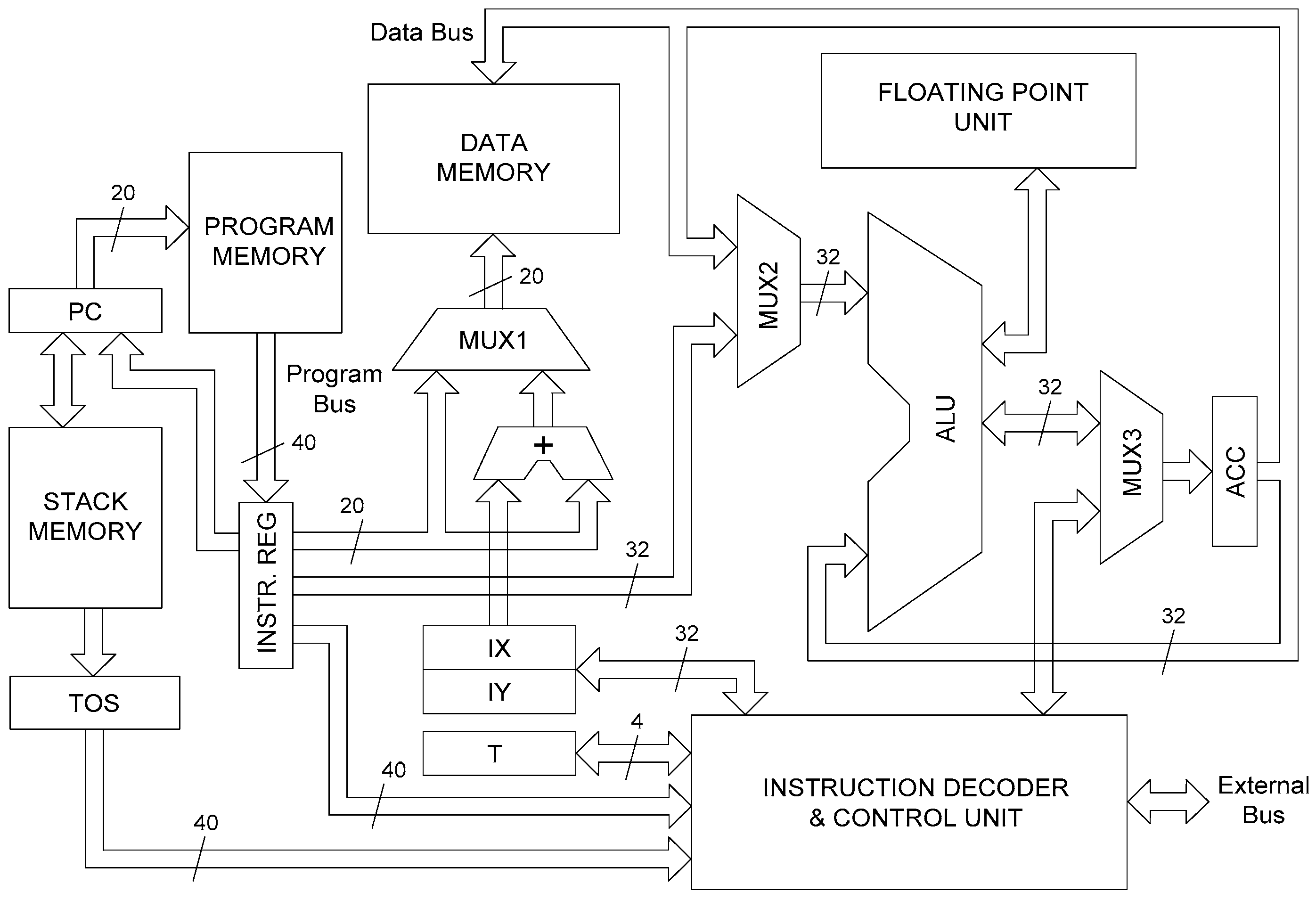
Figure 2.
More detailed part of the architecture involving the program counter and stack memory.
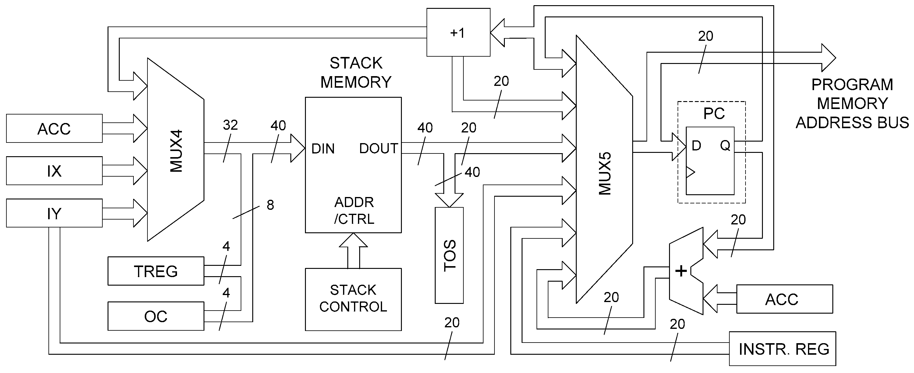
Figure 3.
Architecture of data memory section.

Figure 4.
General format for instructions: (a) for LDA instruction with literals; (b) for other instructions with literals; (c) for instructions with an operand derived from data memory; (d) for CALL and JMP instructions.
Figure 4.
General format for instructions: (a) for LDA instruction with literals; (b) for other instructions with literals; (c) for instructions with an operand derived from data memory; (d) for CALL and JMP instructions.

Figure 5.
Behavioral simulation of an essential part of the code from Table 1, version 2.
Figure 5.
Behavioral simulation of an essential part of the code from Table 1, version 2.

Figure 6.
Simulation involving code that calls the TON timer instance.


Table 1.
Three versions of Equation (1) implementations via the IL processor.
| Version 1: | Version 2: | Version 3: |
|---|---|---|
| LDA A | LDA A | LDA A |
| AND X1 | AND X1 | CAND X1 |
| ST TMP1 | ORP B | LD X2 |
| LDA X2 | ANDNP X2 | OR QT1 |
| OR QT1 | OR QT1 | XOR TRUE |
| XOR TRUE | EDO | CAND B |
| AND B | ORP C | LDA C |
| OR TMP1 | AND QT2 | CAND QT2 |
| ST TMP1 | EDO | CST NB |
| LDA C | EDO | |
| AND QT2 | ST NB | |
| OR TMP1 | ||
| ST NB |
Table 2.
Implementation results of the IL processor.
| FPGA Chip | LUTs | FFs | Max Clock Freq. [MHz] |
|---|---|---|---|
| Spartan-6 XC6SLX100 | 3744 (5.9%) | 2292 (1.8%) | 64.5 |
| Artix-7 XC7A100T | 3675 (5.7%) | 2276 (1.8%) | 74.1 |
| Kintex-7 XC7K325T | 3705 (1.8%) | 2276 (0.6%) | 102.5 |
Table 3.
Execution times of the test algorithms via the IL processor.
| Test Algorithm | Number of Clock Cycles | Time [μs] Spartan-6 @64.286 MHz | Time [μs] Artix-7 @74.099 MHz | Time [μs] Kintex-7 @102.500 MHz |
|---|---|---|---|---|
| LC1 | 218 | 3.39 | 2.94 | 2.13 |
| LC2 | 143 | 2.22 | 1.93 | 1.40 |
| LC3 | 138 | 2.15 | 1.86 | 1.35 |
| LC4 | 119 | 1.85 | 1.61 | 1.16 |
| LC5 | 103 | 1.60 | 1.39 | 1.00 |
| LC6 | 115 | 1.79 | 1.55 | 1.12 |
| LC7 | 70 | 1.09 | 0.94 | 0.68 |
| P1TS | 1779 | 27.67 | 24.01 | 17.36 |
Table 4.
Execution times of the test algorithms via high-performance PAC controllers.
| Test Algorithm | Beckhoff CP6607 @533 MHz (TwinCAT 2) | Beckhoff CX5140 @1.91 GHz (TwinCAT 3) | Raspberry PI 4 @1.8 GHz (CODESYS) | |||
|---|---|---|---|---|---|---|
| Time [μs] | EC | Time [μs] | EC | Time [μs] | EC | |
| LC4 | 1.45 | 773 | 0.31/0.27 | 592/516 | 0.54/0.12 | 972/216 |
| LC6 | 1.32 | 704 | 0.29/0.25 | 554/477 | 0.49/0.10 | 882/180 |
| P1TS | 206.7 | 110,171 | 1.82 | 3476 | 1.06 | 1908 |
Disclaimer/Publisher’s Note: The statements, opinions and data contained in all publications are solely those of the individual author(s) and contributor(s) and not of MDPI and/or the editor(s). MDPI and/or the editor(s) disclaim responsibility for any injury to people or property resulting from any ideas, methods, instructions or products referred to in the content. |
© 2023 by the author. Licensee MDPI, Basel, Switzerland. This article is an open access article distributed under the terms and conditions of the Creative Commons Attribution (CC BY) license (https://creativecommons.org/licenses/by/4.0/).
Share and Cite
MDPI and ACS Style
Hajduk, Z. IEC61131-3 Instruction List Language Processor for FPGAs. Electronics 2023, 12, 4052. https://doi.org/10.3390/electronics12194052
AMA Style
Hajduk Z. IEC61131-3 Instruction List Language Processor for FPGAs. Electronics. 2023; 12(19):4052. https://doi.org/10.3390/electronics12194052
Chicago/Turabian StyleHajduk, Zbigniew. 2023. "IEC61131-3 Instruction List Language Processor for FPGAs" Electronics 12, no. 19: 4052. https://doi.org/10.3390/electronics12194052
Note that from the first issue of 2016, this journal uses article numbers instead of page numbers. See further details here.