Article

A 10-Bit 400 MS/s Dual-Channel Time-Interleaved SAR ADC Based on Comparator Multiplexing

1
Shenzhen International Graduate School, Tsinghua University, Shenzhen 518057, China
2
School of Integrated Circuits, Sun Yat-sen University, Shenzhen 518107, China
3
Department of Elektrotechniek, ESAT-MICAS, KU Leuven, B-3001 Leuven, Belgium
*
Author to whom correspondence should be addressed.
These authors are contributed equally to this work.
Electronics 2023, 12(19), 4062; https://doi.org/10.3390/electronics12194062
Submission received: 19 August 2023 / Revised: 24 September 2023 / Accepted: 26 September 2023 / Published: 27 September 2023
(This article belongs to the Special Issue Advances in Analog and Mixed-Signal Integrated Circuits)

Abstract

:
This paper proposes a 10-bit 400 MS/s dual-channel time-interleaved (TI) successive approximation register (SAR) analog-to-digital converter (ADC) immune to offset mismatch between channels. A novel comparator multiplexing structure is proposed in our design to mitigate comparator offset mismatch between channels and improve ADC dynamic performance. Compared to traditional TI-SAR ADC utilizing offset calibration technique, hardware and power consumption overhead are minimized in our design. In addition, a split capacitive digital-to-analog converter (CDAC) and a double-tail dynamic comparator using the clock decoupling technique were applied to eliminate comparator common mode input voltage shift, ensuring conversion accuracy and boosting speed. A 400 MS/s 10-bit dual-channel TI-SAR ADC with comparator multiplexing was designed in 40 nm CMOS and compared to the conventional one. The simulated ADC ENOB and SFDR with 6σ offset mismatch were improved from 5.0-bit and 32.2 dB to 9.7-bit and 77.2 dB, respectively, confirming the merits of the proposed design compared to current state-of-the-art works.

1. Introduction

Successive approximation register (SAR) analog-to-digital converters (ADCs) are attractive medium resolution applications for the development of the CMOS technologies because of their amplifier-free structure, small area and high energy efficiency [1,2,3,4,5]. For a 10 b resolution, the sampling rate limit of conventional SAR ADC is around 320 MS/s in 20 nm CMOS [5]. To achieve higher speeds while ensuring the precision of ADC, numerous new structures have been recently reported. The 2 b/cycle SAR converts 2-bit data in a single comparison cycle, achieving high speeds by reducing the number of cycles [6]. However, this approach is sensitive to accuracy issues caused by comparator offset and input common-mode (CM) voltage variation due to the use of three comparators. Another high-speed structure is hybrid pipelined-SAR ADC, which divides the entire SAR ADC into multi-stage to operate in parallel [7,8]. While the pipelined-SAR structure can operate at a high sample rate, the design of inter-stage amplifiers in advanced technology poses challenges and requires several calibration techniques to ensure accuracy. These techniques, in turn, result in additional power consumption and occupied area. Subranging SAR ADCs reduce the settling time of the first few MSBs to increase speed while enough redundancy range or compensation are needed because of gain mismatch [9,10,11]. Furthermore, the time-interleaved (TI) SAR ADCs are widely favored for the implementation of high-speed ADCs. In contrast to single-channel ADCs, TI-ADCs interweave multi-channel sub-ADCs to operates at a multiplied sample rate. The sub-ADCs can be implemented by a variety of ADC structures, such as SAR, VCO, pipeline, etc. Since SAR ADCs have the merits of low power and hardware overhead, they are the first choice for time-interleaving with acceptable costs to achieve higher ADC sampling rate. However, inter-channel nonidealities, such as time skews, gain mismatch and comparator offset mismatch introduced by device mismatch, which induce time-dependent errors into the spectrum and limit the accuracy of TI-SAR ADC. Each sub-ADC typically adopts a simplified structure to minimize non-ideal effects and maintain ADC linearity. In TI-SAR ADC, time skews and gain mismatch can be addressed through off-chip digital calibration algorithms and with an on-chip tunable device. However, this article primarily focuses on the offset mismatch resulting from non-idealities in the comparators, as this factor has the potential to impact the dynamic performance of the ADC.
In recent years, numerous methods have been proposed to address the offset mismatch issue in SAR ADC. In [12,13,14], a background calibration was applied in comparators to compensate offset, where the analog calibration voltage needs to be refreshed periodically, occupying additional conversion time and power. Foreground offset calibration, which relies on a differential capacitor array [15,16,17], is another popular approach. Nevertheless, the introduction of additional capacitive load in this method degrades the speed of the comparators. Alternatively, the ADCs discussed in [18,19] utilize CDACs to calibrate offset voltage of high-speed comparator. However, a notable drawback of this approach is the increased area requirement for additional arithmetic circuits.
In this paper, we propose a novel TI-SAR ADC based on comparator multiplexing to address the offset mismatch bottleneck. With a switching circuit, the comparator can operate almost continuously across multiple channels, allowing for a reduction in the number of comparators. This not only lowers the hardware cost but also minimizes the impact of offset. The comparator multiplexing structure enables the use of a small calibration-free comparator, meeting the offset requirements and ensuring ADC dynamic performance without significant power or speed penalties. In this article, we present a 10-bit 400 MS/s TI-SAR ADC implemented in 40 nm CMOS, employing comparator multiplexing. Split CDACs and double-tail dynamic comparators with clock decoupling are applied to eliminate comparator input common mode shift and reduce offset dynamic variation. With the impact of offset, the proposed design shows excellent precision improvement compared to the conventional one.
The remainder of this paper is organized as follows. The design considerations of the proposed comparator multiplexing TI-SAR ADC are introduced in Section 2. Detailed circuit implementation is described in Section 3, followed by the simulated results in Section 4. Finally, a conclusion is drawn in Section 5.

2. Design Considerations

2.1. Conventional Architecture of TI-SAR ADC

Figure 1 illustrates the conventional architecture of N-channel TI-SAR ADC. This architecture comprises an analog interleaver, N sub-SAR ADCs, digital MUX and calibration circuits. A comparator, a differential CDAC, bootstrapped switch and multiple logic circuits form the basic structure of each sub-SAR ADC. The analog interleaver is responsible for feeding the analog input signal into each channel in turn and generating N clock signals with equal phase difference to drive each sub-ADC sequentially. And then, sub-ADCs alternately output digital codes which are selected sequentially by digital MUX and the final digital output will be produced. To mitigate clock skews and inter-channel gain mismatch, tunable capacitors can be incorporated into the clock generator within the interleaver. These capacitors help reduce clock skews using a foreground digital calibration algorithm. However, offset mismatch can vary with input and PVT conditions, thereby limiting the dynamic performance of the ADC. Consequently, considerable effort is typically required to minimize the offset and achieve 10-bit accuracy.

2.2. Offset Mismatch in TI-SAR ADC

As an important module of TI-SAR ADC, the comparators determine the correctness of bit-cycles, and their offset mismatch will introduce periodic error during data conversion [20]. The relationship between the signal-to-noise-and-distortion ratio (SNDR) of the ADC and the offset mismatch of the comparator can be expressed as [18]
S N D R 20 log 10 ( V A 2 σ o m ) 10 log 10 ( 1 1 N )
where V A represents the input signal amplitude and σ o m represents the standard deviation of equivalent offset voltage. N denotes the total number of comparators utilized in the ADC. To illustrate, in a dual-channel TI SAR ADC aiming for a 62 dB SNDR (10-bit resolution) with V A set at 0.9 V, it is necessary to optimize the comparator offset voltage to be less than 0.7 mV. The offset voltage in a comparator is closely related to the threshold-voltage and process transconductance of transistors, as well as the comparator area and overdrive voltage of input pair. This relationship can be expressed as
σ o s σ V t + ( V g s V t h ) i n ( σ K / K + σ W / L / ( W / L ) )
where σ V t , σ K and σ W / L represent standard deviation of transistors threshold-voltage, process transconductance and width-to-length ratio, respectively. Additionally, the process transconductance mismatch is associated with the mobility mismatch σ u , which along with σ V t , are inversely correlated with the square root of device area [20].
σ V t   &   σ u 1 / W L
This means either a large area and power consumption or circuit calibrations will be needed for low-offset comparator design. Additionally, maintaining a constant and low input common mode voltage is crucial to reduce the overdrive voltage and minimize the equivalent input offset voltage. However, this requirement also leads to smaller bias current and longer comparator integration time, creating a trade-off between speed and accuracy. Furthermore, any asymmetry in the layout will introduce offset, the input differential pairs of the comparator should be designed symmetrically enough to cancel parameter gradient.

2.3. Comparator Multiplexing TI-SAR ADC

To enhance the accuracy, optimization area, power consumption and speed, a novel TI-SAR ADC based on comparator multiplexing is proposed. The architecture of this ADC is illustrated in Figure 2. Unlike conventional TI-SAR ADCs, each channel in the proposed one does not contain an individual comparator and corresponding asynchronous comparator clock generator, which are integrated into the comparator array. To mitigate the impact of offset mismatch on ADC accuracy and reduce hardware costs, each comparator is switched to different channels using a bootstrapped (BT) switch array. The kick back noise is reduced by the double-tail structure in the comparator. The output digital code of each channel is integrated by MUX, which is no different from the conventional structure of TI-SAR ADC.
In conventional TI-SAR ADC, offset mismatch can lead to fixed spurious whose amplitude depends on offset mismatch at the integer multiple of each channel sampling frequency [21]. By utilizing a comparator multiplexing architecture, the total comparator number in the proposed ADC is reduced since each comparator can be switched to any channel and remain operational for most of the time. In contrast, conventional ADCs only activate the comparators during the conversion phase and leave them idle during the sampling phase. Consequently, the utilization rate of comparator rises in the proposed structure. Additionally, as the number of comparators and associated asynchronous comparator clock generators decreases, the SNDR of TI-SAR ADC improves according to (1).
In a conventional TI-SAR ADC, when the duty cycle of single channel input clock is denoted as p (where p < 100%, representing conversion phase) and the clock cycle is T, the total conversion time is N × p × T for a N-channel TI-SAR ADC. Based on comparator multiplexing architecture, the number of comparators should be more than N × p (usually N in conventional structure) since the operating time of one comparator is from p × T to T. In the case of a 10-bit resolution, the value of p is typically smaller than 75% to allow for a sufficiently long sampling time, ensuring sampling accuracy. For example, if the duty cycle of conversion phase is 75%, a 64-channel comparator multiplexing TI-SAR ADC would normally use at least 48 comparators. In general, ADCs with higher duty cycle clocks can achieve higher sampling rate. However, they also impose more constraints on the design of the clock generator than the clock of 50% duty cycle [22]. By employing comparator multiplexing, the comparators can switch between every channel and realize the single-comparator operating time of nearly T. Additionally, an additional comparator controlled by pseudo-random signals can be applied in the proposed ADC. This extra comparator randomly switches with a comparator that would be assigned to a new channel in the next conversion. However, random switching would significantly increase the complexity of the switch network. Therefore, further study and analysis are required to extend it to multi-comparator scenarios.

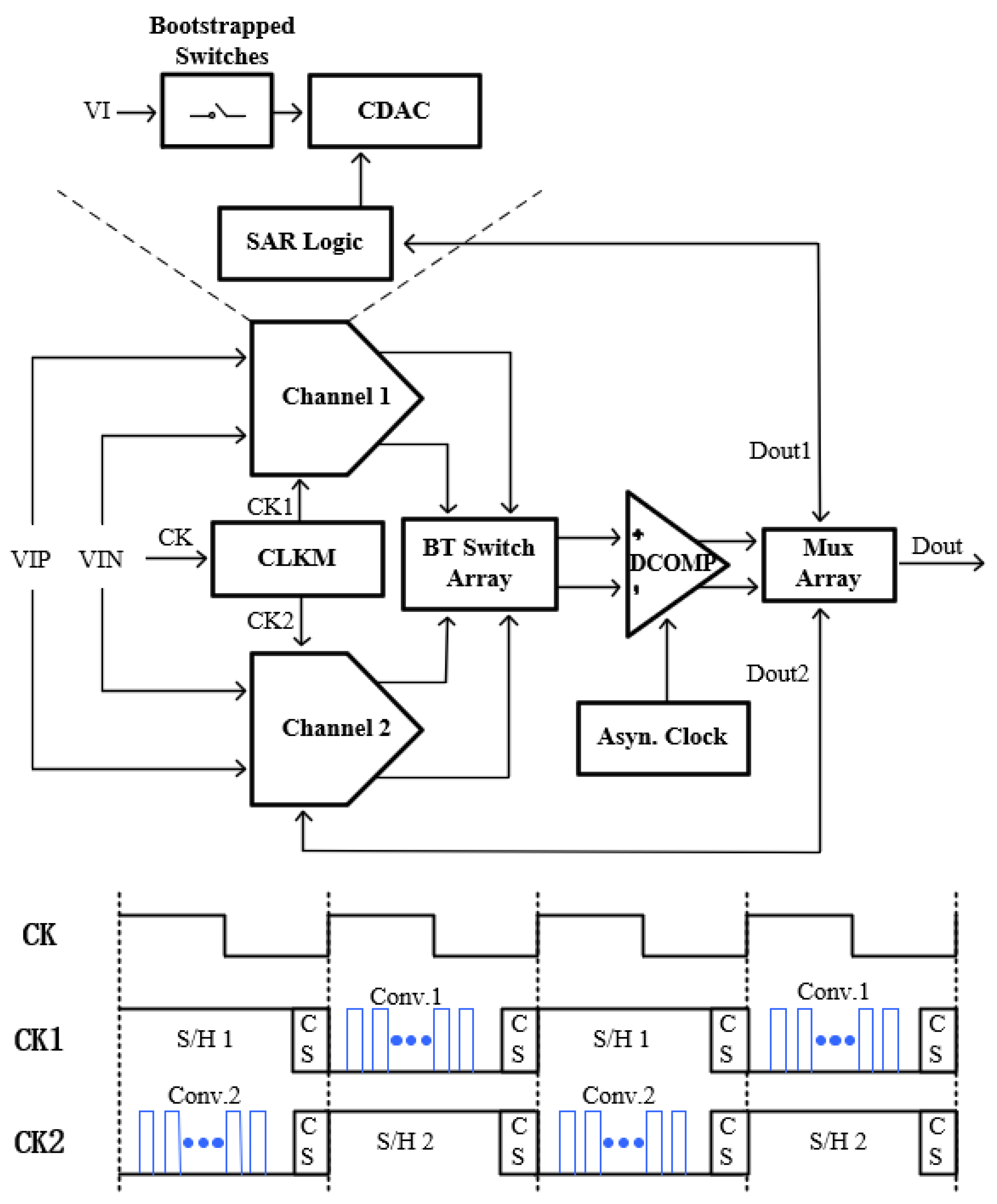
3. Circuit Implementation

3.1. Dual-Channel TI-SAR ADC

In order to highlight the advantages of the comparator multiplexing structure, we propose a dual-channel TI-SAR ADC that utilizes only one comparator, thereby eliminating the impact of offset mismatch. Figure 3 illustrates the architecture and corresponding time diagram of the proposed dual-channel TI-SAR ADC with comparator multiplexing. This TI-SAR ADC configuration comprises a clock divider (CLKM), a multiplexed comparator with bootstrapped switch array, a multiplexer (MUX) array and two channel modules. Each module consists of a differential CDAC, bootstrapped sampling switches and SAR logic control circuit. Note that each channel contains neither a comparator nor an asynchronous comparator clock generator. Two channel modules share a comparator as well as an asynchronous comparator clock generator externally. The CLKM module divides external 400 MHz clock (CK) into two 200 MHz sub-clocks (CK1, CK2) for each channel, which will generate control signals further for switches and MUXs. As a result, no extra control signal generator is needed for the BT switch array and MUX array. The timing diagram in Figure 3 shows the detail of the clock signals. During the high phase of CK1 (channel 1 sampling phase) and the low phase of CK2 (channel 2 data conversion phase), the switchable comparator is connected to channel 2 for data conversion. The sub-clocks have a duty cycle close to 50% for channel sampling, which helps simplify the design of the S/H circuit. Following the sampling phase in each channel, a short switching phase (CS) is allocated for the comparator switching between two channels, without incurring a speed penalty for the ADC.
The switch array is designed to connect the CDAC in each channel to the switchable comparator. In order to ensure signal linearity, differentially bootstrapped switches are used in the array. The control signals of these bootstrapped switches are in phase with the clock of the connected channel. With the exception of the narrow switching phase, the multiplexed comparator remains in a state of continuous comparing and resetting, maximizing the speed of the TI ADC. The multiplexer array is responsible for switching the multiplexed comparator between SAR logic blocks. The SAR logic receives the comparison output from the multiplexed comparator in conversion phase, while blocks the output in sampling phase. After receiving comparison results, the output voltage of the CDAC is updated for the next bit-cycle. Simultaneously, the asynchronous comparator clock generator is triggered by the comparator regeneration indication signal. Once the 10-bit cycles have been accomplished, the asynchronous comparator clock generator generates a complete signal, indicating that the 10-bit digital output (Dout1 or Dout2) were ready. This complete signal will control an output MUX to select channel digital outputs alternately.

3.2. Split CDAC

The architecture of split CDAC in the proposed TI-SAR ADC is displayed in Figure 4. With the split CDAC structure applied, there is almost no VCM shift at the comparator input [23]. To enhance linearity during sampling, the bottom plate sampling technique is employed, which reduces the presence of parasitic MOS capacitors on the sampling node. Bootstrapped switches are utilized to improve sampling accuracy and facilitate the transfer of residue from CDAC to comparators. Figure 5 illustrates the schematic diagram of the proposed SAR logic designed for CDAC configuration. Customized latch and logic circuits are specifically designed to work in conjunction with split CDAC. Numerous control signals are generated to properly configure each capacitor during the conversion and sampling phase. The control relationship between the signal and the capacitor switch is shown at the bottom of Figure 5. A set of four signals, SWPP, SWPN, SWNP, SWNN, determines whether the bottom plate of positive side capacitors should be connected to VRP or VRN. During the sampling phase, the bottom plate is disconnected from the VRP and VRN and connected to the input signal VIN, controlled by the bootstrapped signal. The bottom plate of negative side capacitor is controlled by the inverted signals SWPPB, SWPNB, SWNPB and SWNNB. In the conversion phase, only one of the two split capacitors associated with each bit is activated, either switching to VRP or VRN, based on the final comparison results. The purpose of implementing split CDAC switch logic is to prevent continuous switching of the reference voltage and simplify the design of the reference voltage buffers. The pulse signal SC is generated after each comparison completed and this enables the results of the comparator to set the switching signal. The behavior of the MSB switching control signal during different phases is summarized in Table 1. The discussion above focuses on the SAR logic of the MSB capacitor, which is similar to the other capacitors, except for the LSB capacitor. The LSB capacitor utilizes half of the switching control signal and a simplified SAR logic circuit. Overall, this proposed SAR logic offers reduced hardware overhead and latency compared to traditional static CMOS logic. Moreover, the capacitance weight of each bit in CDAC is differed, therefore the CDAC switch and its driving buffer are carefully sized according to the weight of each bit.

3.3. Unit Capacitor

The unit capacitor is determined so that the thermal noise would not become bottle-neck to proposed structure, assuming the unit capacitance value is C u and the total single-ended sampling capacitance of CDAC is C s . Since a differential structure is employed in proposed SAR ADC, the relationship between these capacitances can be expressed as
C s = 512 C u
The kT/C noise due to the differential structure should be doubled, therefore the noise power generated by the sampling capacitor in SAR ADC is
V n 2 ¯ = 2 k T C s
The sampling noise power must satisfy the SNR requirement by being less than or equal to the quantization noise power
V n 2 ¯ Δ 2 12
Δ = V r 2 N
where V r represents reference voltage. The unit capacitance limited by the requirement of 10-bit resolution with a 0.9 V V r can be expressed as
C u 0.251   fF
Considering the non-ideal factors, such as capacitor mismatch, the proposed unit capacitor value in this design is 2 fF.

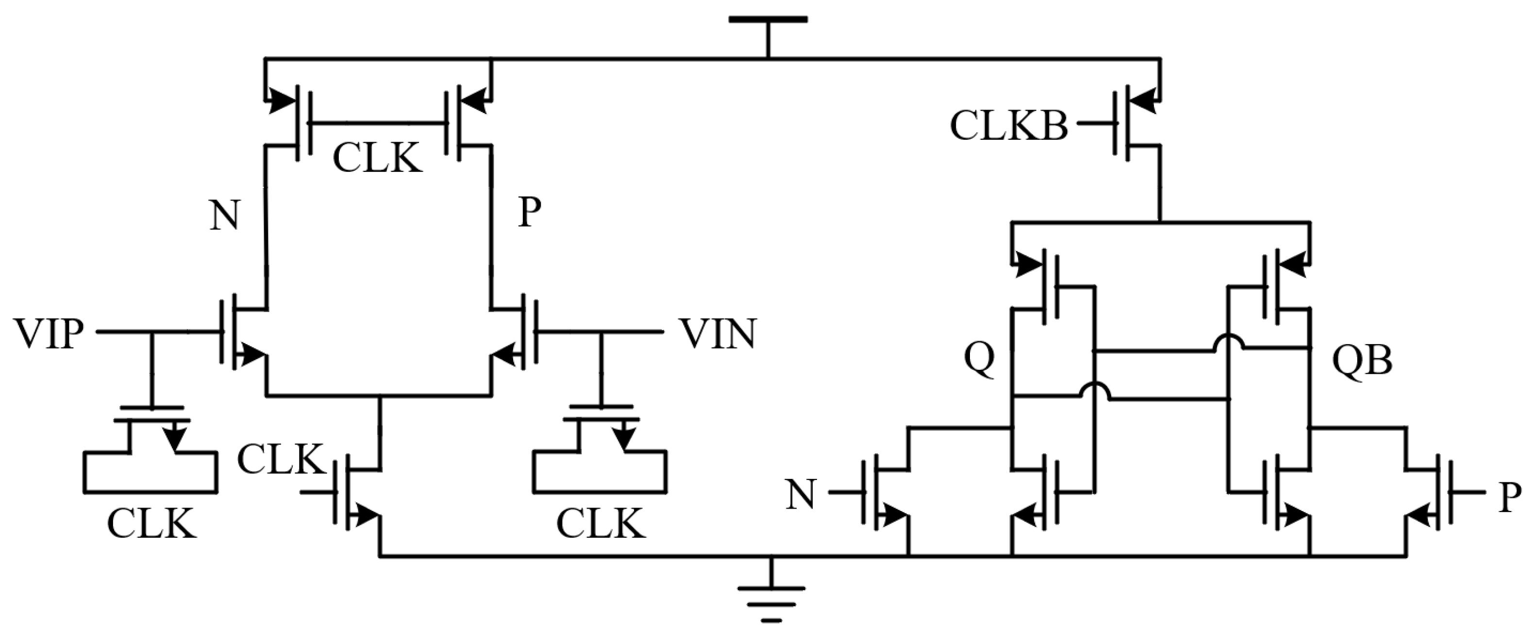
3.4. Double-Tail Dynamic Comparator with Clock Decoupling

Figure 6 presents the schematic of the double-tail dynamic comparator with clock decoupling [24]. A pre-amplifier (with gain of 31.2 dB in our design) would be typically employed as the first stage of comparator. The second stage consists of a latch, which serves to restore the voltage difference obtained from the first stage. During the low phase of the CLK signal, the N and P nodes are charged to a high level, resetting the latch, while the output Q and QN are set to low level. Conversely, during the high phase of the CLK signal, the pre-amplifier stage activates, leading to the discharge of the two output nets of the pre-amplifier. Due to the variation in input voltage value, the discharging rates at N and P points also differ. This voltage discrepancy induces positive feedback in the latch, ultimately causing one output port to stabilize at a high level and the other at a low level. The comparison results, received and restored by MUX, are subsequently processed during the conversion phase of the channel.
Compared to the conventional structure, a decoupling MOS capacitor is included in the gate of input pair. When the comparator clock’s edge rises, the voltage at the input MOS source rapidly decreases, and the falling edge is coupled to the comparator input through a gate-source parasitic capacitor, leading to the additional common-mode and differential-mode signal interference on CDAC. This interference can impact the offset of the comparator and the accuracy of the comparison results. To mitigate this issue, a clock decoupling capacitor is added to the input of comparator. The rising edge of clock is coupled to the CDAC, neutralizing the coupling effect of the falling edge. The clock decoupling capacitor employs a MOS capacitor to match the gate-source parasitic capacitor of input pair. By introducing a properly sized clock decoupling capacitor, the comparator’s accuracy has been significantly enhanced.

3.5. BT Switch

Figure 7 shows the schematic of the BT switch, which connects the channel and the comparator. To ensure the linearity of the results, the BT switch commonly generates a boost signal to maintain a constant turn-on resistance for the switch transistors. The circuit utilizes a sampling clock denoted as CK, with M8 representing the switch transistor. During the low state of CK (known as the holding phase of the BT switch), the bottom plate of the bootstrap capacitor C is connected to ground through M3, while the top plate of C is charged to a high voltage through M4. Simultaneously, M8 turns off, thereby maintaining the output port in its current state. Conversely, during the high state of CK (known as the sampling phase of the BT switch), the bottom plate of C is connected to the source of M8 through M7, and the top plate of C is connected to the gate of M8 through M5. In this phase, the gate-source voltage of M8, which is equal to the voltage difference between the top and bottom plates of C, remains unchanged. In the case of the dual-channel TI-SAR ADC proposed in this paper, both the sampling phase of the BT switch and the conversion phase of the channel share the same clock, eliminating the need for additional signal generation.

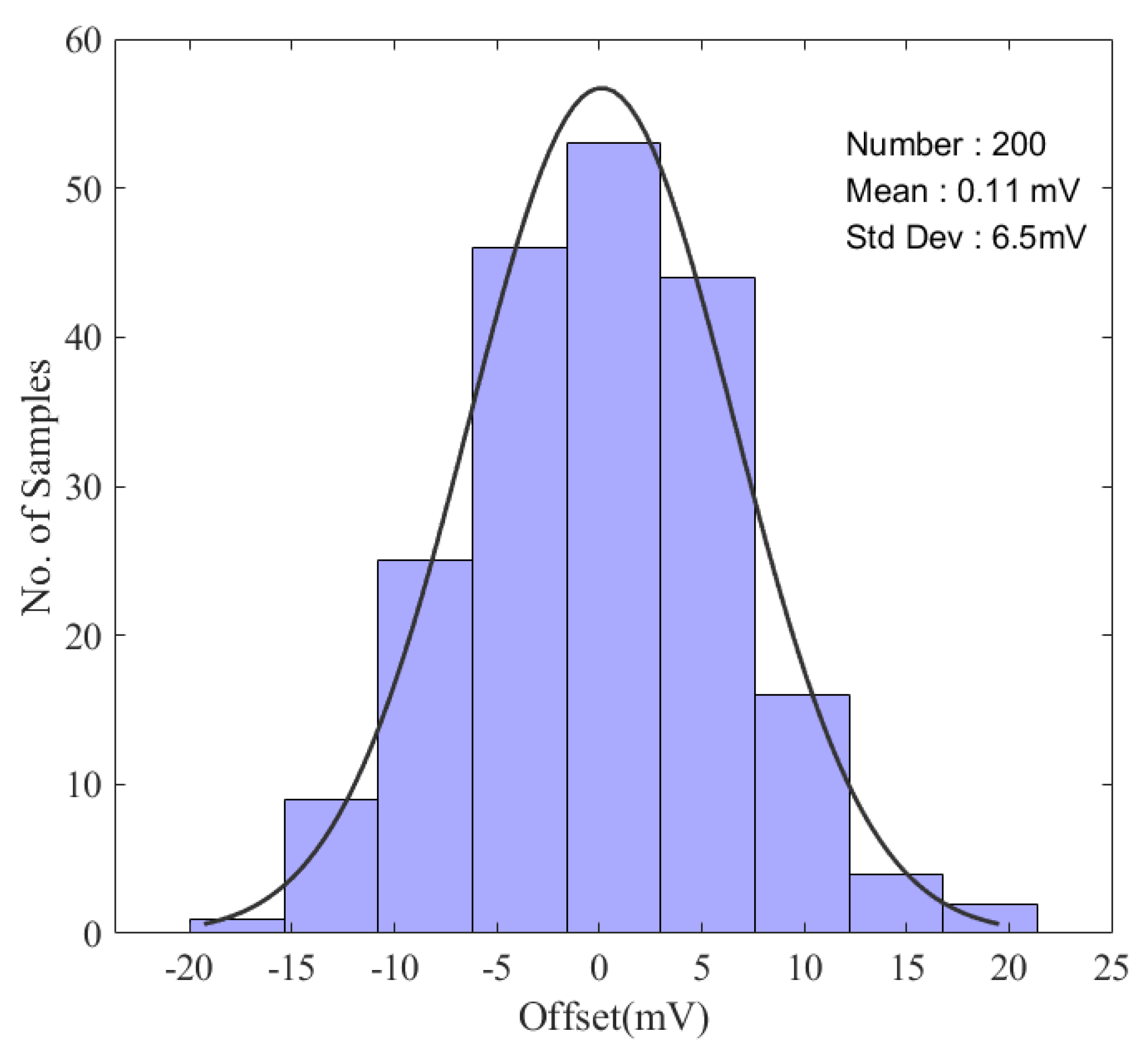
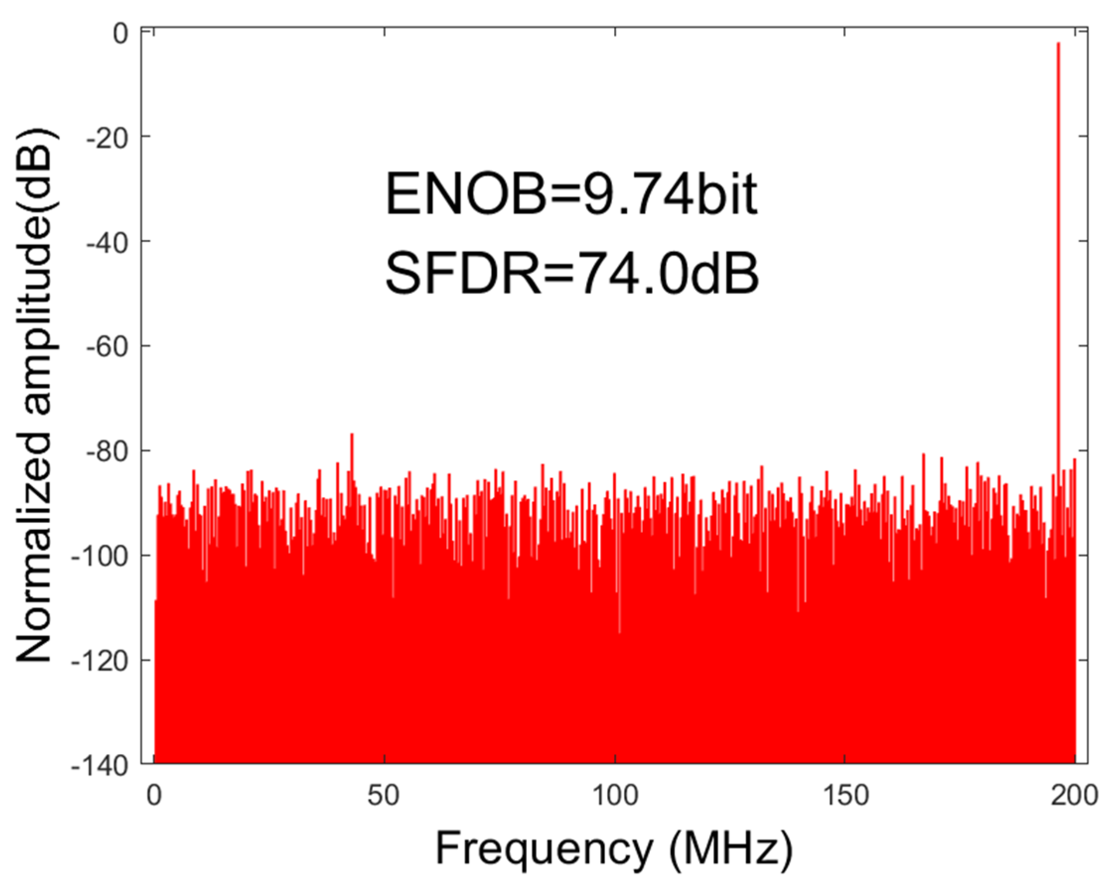
4. Simulation Results

To validate the proposed technique, two 10-bit 400 MS/s TI-SAR ADCs were fabricated using 40 nm CMOS. One ADC incorporates the proposed comparator multiplexing approach, while the other follows conventional design principles. The same circuit modules, e.g., dual-channel structure, double-tail dynamic comparators, CDACs and the same 0.9 V supplies were applied in these TI-SAR ADCs. The only differences between the two ADCs are the number of comparators and the associated control circuits.
The results of the Monte Carlo simulation consisting of 200 runs are presented in Figure 8. The standard deviation (σ) of the comparator offset voltage is approximately 6.5 mV. However, this value falls short of meeting the requirements of a conventional 10-bit TI-SAR ADC, as stated in Equation (1). Nonetheless, the compact size of the comparators, along with the implementation of an asynchronous comparator clock generator, account for only 19% and 12% of total power consumption, respectively. Figure 9 illustrates the simulated ENOBs and SFDRs for both the proposed and the conventional TI-SAR ADCs, considering different levels of comparator offset mismatch. The results indicate that the proposed dual-channel TI-SAR ADC with comparator multiplexing exhibits immunity to offset mismatch, while the conventional one is sensitive to it. Furthermore, Figure 10 showcases the simulated spectra of the proposed and the conventional ADCs when subjected to 6σ comparator offset and Nyquist input. The proposed comparator multiplexing architecture significantly enhances the ADC ENOB from 5.0-bit to 9.7-bit and boosts the SFDR from 32.2 dB to 77.2 dB, with a mere 9.1% increase in power consumption.
The standard deviation (σ) of the capacitor used in BT switch is approximately 100 aF. Considering the mismatch among BT switches, a variation of 6σ (approximately 0.6fF) is introduced for the capacitor C, as well as 10% scale mismatch of the switch transistor M8. The simulated spectrum of proposed ADCs, considering the mismatch among BT switches, is presented in Figure 11. Notably, no noticeable performance degradation was observed due to the mismatch of BT switches. Table 2 summarizes the proposed TI -SAR ADC and compares it to the state-of-the-art works. Our work achieves an outstanding FOM of 7.2 fJ/conv.-step.

5. Conclusions

This paper presents a novel dual-channel 10-bit 400 MS/s TI-SAR ADC featuring a switchable calibration-free comparator. The proposed dual-channel comparator multiplexing ADC structure eliminates comparator offset mismatch, leading to a significant improvement in ADC dynamic performance without incurring substantial hardware or power overhead. To improve accuracy, the design incorporates split CDAC and clock decoupling techniques. BT switches were utilized to connect channels and multiplexing comparators while maintaining a constant turn-on resistance in the switch transistors. Simulation results demonstrated a 6σ offset mismatch. The proposed 400 MS/s dual-channel TI-SAR ADC achieved 9.7-bit ENOB and 77.2 dB SFDR with an excellent FOM of 7.2 fJ/conv.-step.

Author Contributions

Conceptualization, C.W., Z.Y. and X.X.; Funding acquisition, X.X.; Methodology, C.W., Z.Y. and X.X.; Validation, C.W.; Writing—original draft, Z.Y.; Writing—review and editing, X.X., Q.D., X.Z. and G.G. All authors have read and agreed to the published version of the manuscript.

Funding

This work was supported in part by the National Natural Science Foundation of China (61874063), the Guangdong Key Area R&D Program (2019B010143003), the Shenzhen Science and Technology innovative committee (GJHZ20200731095609029, WDZC20200820160650001), the Chongqing Science and Technology Commission (cstc2018jszx-cyztzxX0052) and SIGS, Tsinghua University (HW2021014).

Data Availability Statement

Data sharing not applicable.

Acknowledgments

The authors would like to thank all of the editors and reviewers for their valuable comments.

Conflicts of Interest

The authors declare no conflict of interest.

References

  1. Liu, C.C.; Chang, S.J.; Huang, G.Y.; Lin, Y.Z.; Huang, C.M.; Huang, C.H.; Bu, L.; Tsai, C.C. A 10b 100MS/s 1.13mW SAR ADC with binary-scaled error compensation. In Proceedings of the 2010 IEEE International Solid-State Circuits Conference—(ISSCC), San Francisco, CA, USA, 7–11 February 2010; pp. 386–387. [Google Scholar]
  2. Liu, C.C.; Kuo, C.H.; Lin, Y.Z. A 10 bit 320 MS/s Low-Cost SAR ADC for IEEE 802.11ac Applications in 20 nm CMOS. IEEE J. Solid-State Circuits 2015, 50, 2645–2654. [Google Scholar] [CrossRef]
  3. Chan, C.H.; Zhu, Y.; Li, C.; Zhang, W.H.; Ho, I.M.; Wei, L.; Seng-Pan, U.; Martins, R.P. 60-dB SNDR 100-MS/s SAR ADCs with Threshold Reconfigurable Reference Error Calibration. IEEE J. Solid-State Circuits 2017, 52, 2576–2588. [Google Scholar] [CrossRef]
  4. Qiu, L.; Tang, K.; Zheng, Y.; Siek, L. A Flexible-Weighted Nonbinary Searching Technique for High-Speed SAR-ADCs. IEEE Trans. Very Large Scale Integr. (VLSI) Syst. 2016, 24, 2808–2812. [Google Scholar] [CrossRef]
  5. Zhu, Y.; Chan, C.H.; Seng-Pan, U.; Martins, R.P. An 11b 450 MS/s Three-Way Time-Interleaved Subranging Pipelined-SAR ADC in 65 nm CMOS. IEEE J. Solid-State Circuits 2016, 51, 1223–1234. [Google Scholar] [CrossRef]
  6. Song, J.; Tang, X.; Sun, N. A 10-b 2b/cycle 300MS/s SAR ADC with a single differential DAC in 40nm CMOS. In Proceedings of the 2017 IEEE Custom Integrated Circuits Conference (CICC), Austin, TX, USA, 30 April–3 May 2017; pp. 1–4. [Google Scholar]
  7. Moon, K.J.; Kang, H.W.; Jo, D.S.; Kim, M.Y.; Baek, S.Y.; Choi, M.; Ko, H.J.; Ryu, S.T. A 9.1 ENOB 21.7fJ/conversion-step 10b 500MS/s single-channel pipelined SAR ADC with a current-mode fine ADC in 28nm CMOS. In Proceedings of the 2017 Symposium on VLSI Circuits, Kyoto, Japan, 5–8 June 2017; pp. C94–C95. [Google Scholar]
  8. Kull, L.; Luu, D.; Menolfi, C.; Braendli, M.; Francese, P.A.; Morf, T.; Kossel, M.; Yueksel, H.; Cevrero, A.; Ozkaya, I.; et al. 28.5 A 10b 1.5GS/s pipelined-SAR ADC with background second-stage common-mode regulation and offset calibration in 14nm CMOS FinFET. In Proceedings of the 2017 IEEE International Solid-State Circuits Conference (ISSCC), San Francisco, CA, USA, 5–9 February 2017; pp. 474–475. [Google Scholar]
  9. Yu, Q.; Zhou, X.; Hu, K.; Huang, Z.; Chen, H.; Si, X.; Yang, J.; Li, Q. A 9.08 ENOB 10b 400MS/s Subranging SAR ADC with Subsetted CDAC and PDAS in 40nm CMOS. In Proceedings of the ESSCIRC 2021—IEEE 47th European Solid State Circuits Conference (ESSCIRC), Grenoble, France, 13–22 September 2021; pp. 391–394. [Google Scholar]
  10. Wang, J.C.; Li, B.Y.; Kuo, T.H. A 9.8-fJ/conv.-step FoMW 8b 2.5-GS/s Single-Channel CDAC-Assisted Subranging ADC with Reference-Embedded Comparators. In Proceedings of the 2022 IEEE Symposium on VLSI Technology and Circuits (VLSI Technology and Circuits), Honolulu, HI, USA, 12–17 June 2022; pp. 92–93. [Google Scholar]
  11. Hu, Y.S.; Shih, C.H.; Tai, H.Y.; Chen, H.W.; Chen, H.S. A 0.6V 6.4fJ/conversion-step 10-bit 150MS/s subranging SAR ADC in 40nm CMOS. In Proceedings of the 2014 IEEE Asian Solid-State Circuits Conference (A-SSCC), KaoHsiung, Taiwan, 10–12 November 2014; pp. 81–84. [Google Scholar]
  12. Chan, C.H.; Zhu, Y.; Zhang, W.H.; Seng-Pan, U.; Martins, R.P. A Two-Way Interleaved 7-b 2.4-GS/s 1-Then-2 b/Cycle SAR ADC with Background Offset Calibration. IEEE J. Solid-State Circuits 2018, 53, 850–860. [Google Scholar] [CrossRef]
  13. Fan, Q.; Hong, Y.; Chen, J. A Time-Interleaved SAR ADC with Bypass-Based Opportunistic Adaptive Calibration. IEEE J. Solid-State Circuits 2020, 55, 2082–2093. [Google Scholar] [CrossRef]
  14. Li, D.; Zhu, Z.; Liu, J.; Zhuang, H.; Yang, Y.; Sun, N. A 7-bit 900-MS/s 2-Then-3-bit/cycle SAR ADC with Background Offset Calibration. IEEE J. Solid-State Circuits 2020, 55, 3051–3063. [Google Scholar] [CrossRef]
  15. Chung, Y.H.; Hsu, Y.M. A 12-Bit 100-MS/s Subrange SAR ADC with a Foreground Offset Tracking Calibration Scheme. IEEE Trans. Circuits Syst. II Express Briefs 2019, 66, 1094–1098. [Google Scholar] [CrossRef]
  16. Ding, M.; Harpe, P.; Liu, Y.H.; Busze, B.; Philips, K.; De Groot, H. A 46 μW 13 b 6.4 MS/s SAR ADC with Background Mismatch and Offset Calibration. IEEE J. Solid-State Circuits 2017, 52, 423–432. [Google Scholar] [CrossRef]
  17. Hsu, C.W.; Chang, S.J. A 1.6-GS/s 8b Flash-SAR Time-Interleaved ADC with Top-Plate Residue Based Gain Calibration. In Proceedings of the 2021 IEEE International Symposium on Circuits and Systems (ISCAS), Daegu, Republic of Korea, 22–28 May 2021; pp. 1–5. [Google Scholar]
  18. Zhu, Y.; Chan, C.H.; Seng-Pan, U.; Martins, R.P. A 10-bit 500-MS/s Partial-Interleaving Pipelined SAR ADC with Offset and Reference Mismatch Calibrations. IEEE Trans. Very Large Scale Integr. Syst. 2017, 25, 354–363. [Google Scholar] [CrossRef]
  19. Lopez-Angulo, A.; Gines, A.; Peralias, E. Calibration of Capacitor Mismatch and Static Comparator Offset in SAR ADC with Digital Redundancy. In Proceedings of the 2020 IEEE International Symposium on Circuits and Systems (ISCAS), Seville, Spain, 12–14 October 2020; pp. 1–5. [Google Scholar]
  20. Bichan, M.; Carusone, A.C. The effect of redundancy on mismatch-induced offset and random noise in a dynamic comparator. In Proceedings of the 2009 Ph.D. Research in Microelectronics and Electronics, Cork, Ireland, 12–17 July 2009; pp. 180–183. [Google Scholar]
  21. Kurosawa, N.; Kobayashi, H.; Maruyama, K.; Sugawara, H.; Kobayashi, K. Explicit analysis of channel mismatch effects in time-interleaved ADC systems. IEEE Trans. Circuits Syst. I Fundam. Theory Appl. 2001, 48, 261–271. [Google Scholar] [CrossRef]
  22. Kull, L.; Pliva, J.; Toifl, T.; Schmatz, M.; Francese, P.A.; Menolfi, C.; Brändli, M.; Kossel, M.; Morf, T.; Andersen, T.M.; et al. Implementation of Low-Power 6–8 b 30–90 GS/s Time-Interleaved ADCs with Optimized Input Bandwidth in 32 nm CMOS. IEEE J. Solid-State Circuits 2016, 51, 636–648. [Google Scholar] [CrossRef]
  23. Tripathi, V.; Murmann, B. An 8-bit 450-MS/s single-bit/cycle SAR ADC in 65-nm CMOS. In Proceedings of the 2013 Proceedings of the ESSCIRC (ESSCIRC), Bucharest, Romania, 16–20 September 2013; pp. 117–120. [Google Scholar]
  24. Chen, J.; Xing, X.; Yang, Z.; Feng, H.; Wang, Z. A 10-bit 200MS/s SAR ADC with reference buffer in 40nm CMOS. In Proceedings of the 2020 IEEE 15th International Conference on Solid-State & Integrated Circuit Technology (ICSICT), Kunming, China, 3–6 November 2020; pp. 1–3. [Google Scholar]
  25. Shen, L.; Li, F.; Wang, Z. A 10b 50 MS/s single-Channel asynchronous SAR ADC with two alternate comparators and comparator calibration. In Proceedings of the 2019 IEEE International Conference on Integrated Circuits, Technologies and Applications (ICTA), Chengdu, China, 13–15 November 2019; pp. 35–36. [Google Scholar]
  26. Yasin Adıyaman, M.; Karalar, T.C. Time-interleaved SAR ADC design with background calibration. Int. J. Circuit Theory Appl. 2020, 48, 321–334. [Google Scholar] [CrossRef]
  27. Xing, D.; Zhu, Y.; Chan, C.H.; Maloberti, F.; Seng-Pan, U.; Martins, R.P. Design of a High-Speed Time-Interleaved Sub-Ranging SAR ADC with Optimal Code Transfer Technique. IEEE Trans. Circuits Syst. I Regul. Pap. 2019, 66, 489–501. [Google Scholar] [CrossRef]
Figure 1. The conventional architecture of N-channel TI-SAR ADC.
Electronics 12 04062 g001
Figure 2. The architecture of N-channel comparator multiplexing TI-SAR ADC.
Electronics 12 04062 g002
Figure 3. The architecture and corresponding time diagram of the proposed dual-channel TI-SAR ADC with comparator multiplexing.
Electronics 12 04062 g003
Figure 4. The architecture of split CDAC in the proposed TI-SAR ADC.
Electronics 12 04062 g004
Figure 5. The schematic of the proposed SAR logic used to set the CDAC.
Electronics 12 04062 g005
Figure 6. The schematic of the double-tail dynamic comparator with clock decoupling.
Electronics 12 04062 g006
Figure 7. The schematic of the BT switch connecting the channel with the comparator.
Electronics 12 04062 g007
Figure 8. 200-run Monte Carlo simulation results showing comparator offset caused by random device mismatch.
Electronics 12 04062 g008
Figure 9. Simulated ENOBs and SFDRs of the proposed and the conventional TI-SAR ADCs with different comparator offset mismatches.
Electronics 12 04062 g009
Figure 10. The simulated spectra of the proposed and the conventional TI SAR ADCs with 6σ offset mismatch and 198.8 MHz input. (a) the proposed structure; (b) the conventional structure.
Electronics 12 04062 g010
Figure 11. The simulated spectrum of the proposed TI-SAR ADCs with the mismatch among BT switches.
Electronics 12 04062 g011
Table 1. The status of the MSB switching control signal at different phases.
BitPhaseCK1/2BTSWPPSWNNSWPNSWNP
MSBSampling111001
Charge transfer000101
conversionQ = 1001111
Q = 0000000
Table 2. Performance comparison with the state-of-the-art SAR ADCs.
SpecificationsThis Work *,a[5] b[6] b[18] b[25] a[26] a[27] b
Technology40 nm40 nm65 nm40 nm65 nm180 nm40 nm65 nm
ArchitectureComp. mux.
TI-SAR
TI-SARTI- Subranging Pipe-SAR2 b/cycle SAR Partial-Interleaving Pipe-SARTwo Comp. SARTI-
SAR
TI- Subranging SAR
Num. of channels22311/21182
Calibrationnonoyesnoyesyesyesyes
Resolution (bit)1010111010101010
Sampling Rate (MS/s)400400450300500502000700
SNDR @Nyq. (dB)60.2
(w/offset)
31.9
(w/offset)
56.247.052.961.352.353.3
SFDR @Nyq. (dB)77.232.265.563.066.075.362.070.4
Power (mW)2.402.207.402.108.206.6010.59.50
FOM @Nyq. (fJ/conv.-step)7.2171.931.238.346.0139.424.236.0
* Simulation results with 6σ offset mismatch. a Simulated result. b Measured results.
Disclaimer/Publisher’s Note: The statements, opinions and data contained in all publications are solely those of the individual author(s) and contributor(s) and not of MDPI and/or the editor(s). MDPI and/or the editor(s) disclaim responsibility for any injury to people or property resulting from any ideas, methods, instructions or products referred to in the content.

